

现货库存、技术资料、百科信息、热点资讯,精彩尽在鼎好!
Step Down Voltage-Regulator with Reset
Datasheet
1Overview
1.1 Features
• Step down converter
• Supply Over- and Under-Voltage-Lockout
• Low Output voltage tolerance
• Output Overvoltage Lockout
• Output Under-Voltage-Reset with delay
• Overtemperature Shutdown
• Wide Ambient operation range -40°C to 125°C
• Wide Supply voltage operation range
• Very low current consumption
• Very small P-DSO-8 SMD package
Type Ordering Code Package
P-DSO-8-3
TLE 6365
TLE 6365 G Q67006-A9515 P-DSO-8-3
Functional description
General
The TLE 6365 G is a power supply circuit especially designed for automotive
applications.
The device is based on Infineon’s power technology SPT
®
which allows bipolar and
CMOS control circuitry to be integrated with DMOS power devices on the same
monolithic circuitry.
The TLE 6365 G contains a buck converter and a power on reset feature to start up the
system.
The very small P-DSO-8-3 SMD package meets the application requierements.
It delivers a precise 5V fully short circuit protected output voltage.
Furthermore, the build-in features like under- and overvoltage lockout for supply- and
output-voltage and the overtemperature shutdown feature increase the reliability of the
TLE 6365 G supply system.
Data Sheet Rev. 1.7 1 2003-06-02
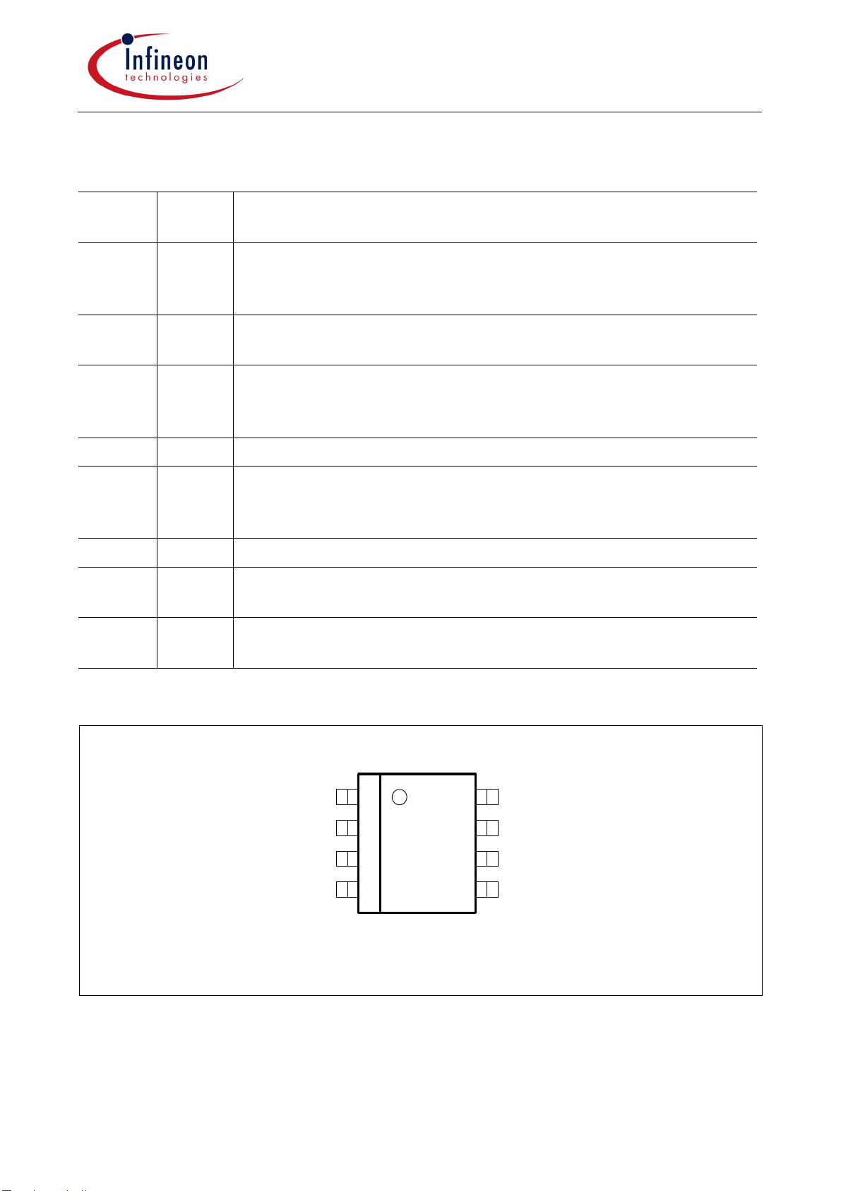
1.2 Pin Definitions and Functions
TLE 6365
Pin
Symbol Function
No
1R Reference Input; an external resistor from this pin to GND
determines the reference current and so the oscillator / switching
frequency
2RO Reset Output; open drain output from reset comparator with an
internal pull up resistor
3BUCBuck-Converter Compensation Input; output of internal error
amplifier; for loop-compensation and therefore stability connect
an external R-C-series combination to GND.
4GNDGround; analog signal ground
5 V
CC
Output Voltage Input; feedback input (with integrated resistor
devider) and logic supply input; external blocking capacitor
necessary
7BUOBuck Converter Output; source of the integrated power-DMOS
6BDSBuck Driver Supply Input; voltage to drive the buck converter
powerstage
8 V
S
Supply Voltage Input; buck converter input voltage; external
blocking capacitor necessary.
Pin Configuration
R
18
RO BUO
BUC BDS
GND
2
3
4
P-DSO-8-3
Figure 1 Pin Configuration (top view)
V
S
7
6
5
V
CC
Data Sheet Rev. 1.7 2 2003-06-02
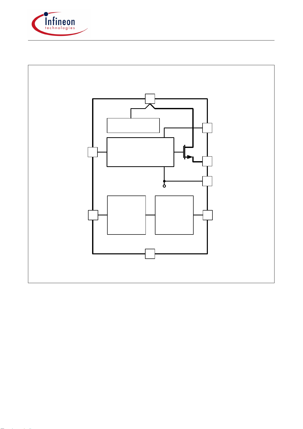
1.3 Block Diagram
TLE 6365
V
S
8
BUC
Biasing and V
3
Buck
Converter
TLE 6365 G
Reference
R
1
Current
Generator
and
Oscillator
REF
4
GND
V
internal
Undervoltage
Reset
Generator
BDS
6
BUO
7
V
CC
5
RO
2
Figure 2 Block Diagram
Data Sheet Rev. 1.7 3 2003-06-02

1.4 Absolute Maximum Ratings
Parameter Symbol Limit Values Unit Remarks
min. max.
Voltages
TLE 6365
Supply voltage V
Buck output voltage V
Buck driver supply voltage V
Buck compensation input
V
S
BUO
BDS
BUC
– 0.3 46 V
– 1 46 V
– 0.3 55 V
– 0.3 6.8 V
voltage
Logic supply voltage V
Reset output voltage V
Current reference voltage V
CC
RO
R
– 0.3 6.8 V
– 0.3 6.8 V
– 0.3 6.8 V
ESD-Protection (Human Body Model; R=1,5kΩ; C=100pF)
all pins to GND V
HBM
–2 2 kV
Temperatures
Junction temperature T
Storage temperature
j
T
stg
– 40 150 ° C–
– 50 150 ° C–
Note: Stresses above those listed here may cause permanent damage to the device.
Exposure to absolute maximum rating conditions for extended periods may affect
device reliability.
Data Sheet Rev. 1.7 4 2003-06-02

1.5 Operating Range
Parameter Symbol Limit Values Unit Remarks
min. max.
TLE 6365
Supply voltage V
Supply voltage V
Supply voltage V
Supply voltage V
Buck output voltage V
Buck driver supply voltage V
Buck compensation input
V
voltage
Logic supply voltage V
Reset output voltage V
Current reference voltage V
Junction temperature
T
Thermal Resistance
S
S
S
S
BUO
BDS
BUC
CC
RO
CREF
j
– 0.3 40 V
535VV
4.5 36 V V
increasing
S
decreasing
S
– 0.3 4.5 V Buck-Converter
OFF
– 0.6 40 V
– 0.3 50 V
03.0V
4.0 6.2 V
– 0.3 V
CC
V
+0.3
01.23V
– 40 150 ° C
Junction ambient R
Data Sheet Rev. 1.7 5 2003-06-02
thj-a
180 K/W –

TLE 6365
1.6 Electrical Characteristics
V
8V<
all voltages with respect to ground; positive current defined flowing into the pin; unless otherwise specified
No. Parameter Symbol Limit Values Unit Test
1.6.1 Current Consumption
< 35V; 4.75V< VCC<5.25V; - 40°C< Tj<150°C; RR=47kΩ;
S
min. typ. max
.
Condition
1.6.1.1 Current consumption;
I
S
see applicatiopn circuit
1.6.1.2 Current consumption;
I
S
see applicatiopn circuit
1.6.2 Under- and Over-Voltage Lockout at
1.6.2.1 UV ON voltage;
V
SUVON
buck conv. ON
1.6.2.2 UV OFF voltage;
V
SUVOFF
buck conv. OFF
1.6.2.3 UV Hysteresis voltage V
1.6.2.4 OV OFF voltage;
SUVHY
V
SOVOFF
buck conv. OFF
1.6.2.5 OV ON voltage;
V
SOVON
buck conv. ON
1.6.2.6 OV Hysteresis voltage V
SUVHY
1.5 4 mA ICC=0mA
510mAICC=400mA
V
S
4.0 4.5 5.0 V V
S
increasing;
3.5 4.0 4.5 V V
S
decreasing
0.2 0.5 1.0 V HY = ON OFF
34 37 40 V V
S
increasing
30 33 36 V V
S
decreasing
1.5 4 10 V HY = OFF ON
1.6.3 Over-Voltage Lockout at
1.6.3.1 OV OFF voltage;
buck conv. OFF
1.6.3.2 OV ON voltage;
buck conv. ON
1.6.3.3 OV Hysteresis voltage V
V
CC
V
CCOVOFF
V
CCOVON
CCOVHY
5.5 6.0 6.5 V V
CC
increasing
5.25 5.75 6.25 V V
CC
decreasing
0.10 0.25 0.50 V HY = OFF ON
Data Sheet Rev. 1.7 6 2003-06-02

TLE 6365
1.6 Electrical Characteristics (cont’d)
V
8V<
all voltages with respect to ground; positive current defined flowing into the pin; unless otherwise specified
No. Parameter Symbol Limit Values Unit Test
< 35V; 4.75V< VCC<5.25V; - 40°C< Tj<150°C; RR=47kΩ;
S
min. typ. max
.
Condition
1.6.4 Buck-Converter; BUO, BDS, BUC and V
1.6.4.1 Logic supply voltage V
1.6.4.2 Efficiency; see. appl. circuit
1.6.4.3 Power-Stage ON
η
R
CC
BUON
4.9 5.1 V
resistance
1.6.4.4 Power-Stage ON
R
BUON
resistance
1.6.4.5 Buck overcurrent threshold I
1.6.4.6 Input current on pin V
CC
1.6.4.7 Buck Gate supply voltage;
V
=VS - V
BGS
BDS
BUOC
I
CC
V
BGS
0.7 0.9 1.2 A
57.210V
CC
1mA < ICC<
400mA;
see. appl.
circuit
85 % I
CC
400mA;
V
0.38 0.5 Ω Tj=25°C;
I
BUO
1.0 Ω I
BUO
500 µA VCC=5V
=
= 14V
S
= 0.6A
= 0.6A
1.6.5 Reference Input ; R
(Oscillator; Timebase for Buck-Converter and Reset)
1.6.5.1 Voltage on pin R
1.6.5.2 Oscillator frequency
1.6.5.3 Oscillator frequency
1.6.5.4 Cycle time for reset timing
Data Sheet Rev. 1.7 7 2003-06-02
V
f
OSC
f
OSC
t
CYL
R
1.4 V RR = 100kΩ
85 95 105 kHz Tj = 25°C
75 115 kHz
1mst
CYL
f
OSC
= 100 /

TLE 6365
1.6 Electrical Characteristics (cont’d)
8V<
V
< 35V; 4.75V< VCC<5.25V; - 40°C< Tj<150°C; RR=47kΩ;
S
all voltages with respect to ground; positive current defined flowing into the pin; unless otherwise specified
No. Parameter Symbol Limit Values Unit Test
min. typ. max
.
1.6.6 Reset Generator; RO
Condition
1.6.6.1 Reset threshold;
V
decreasing
CC
V
1.6.6.2 Reset low voltage V
1.6.6.3 Reset low voltage V
1.6.6.4 Reset high voltage V
1.6.6.5 Reset pull up curent I
1.6.6.6 Reset Reaction time
t
RT
ROL
ROL
ROH
RO
RR
4.50 4.65 4.75 V VRO H to L
or L to H
transition;
V
remains
RO
low down to
V
>1V
CC
-0.20.4VI
-0.20.4VI
=1mA;
ROL
2.5V < V
< V
RT
=0.2mA
ROL
CC
;
V
CC
-0.1
V
CC
+0.1
1V < V
V
RT
VI
ROH
<
CC
= 0mA
240 µΑ 0V < VRO<
4V
10 40 90 µs V
CC
< V
RT
1.6.6.7 Power-up reset delay time t
RD
128 t
CYL
VCC ≥ 4.8 V
1.6.7 Thermal Shutdown (Boost and Buck-Converter OFF)
1.6.7.1 Thermal shutdown junction
T
jSD
150 175 200 ° C
temperature
1.6.7.2 Thermal switch-on junction
T
jSO
120 170 °C
temperature
1.6.7.3 Temperature hysteresis ∆
Data Sheet Rev. 1.7 8 2003-06-02
T 30 K

TLE 6365
2 Circuit Description
Below some important sections of the TLE 6365 are described in more detail.
Power On Reset
In order to avoid any system failure, a sequence of several conditions has to be passed.
V
In case of
pin RO to reset an external microcontroller. When the level of
threshold
before switching to HIGH. If VCC drops below the reset threshold VRT for a time extending
the reset reaction time
period
t
RD
“glitches” on the
power down (VCC < VRT for t > tRR) a logic LOW signal is generated at the
CC
V
reaches the reset
CC
V
, the signal at RO remains LOW for the Power-up reset delay time t
RT
t
, the reset circuit is activated and a power down sequence of
RR
RD
is initiated. The reset reaction time tRR avoids wrong triggering caused by short
V
-line.
CC
< t
V
CC
RO
V
PG
V
RT
H
L
typ.4,70V
typ.4,65V
1V
invalid
ON DelayStart Up
t
RD
RR
t
RR
< t
RD
ON Delay
started stopped
Power Sart-Up Normal NormalFailed N Failed
Figure 3 Reset Function
ON Delay
t
invalidinvalid
t
RD
t
Data Sheet Rev. 1.7 9 2003-06-02

TLE 6365
Buck Converter
A stabilized logic supply voltage (typ. 5 V) for general purpose is realized in the system
L
by a buck converter. An external buck-inductance
DMOS power transistor with the programmed frequency (pin R).
The buck converter uses the temperature compensated bandgap reference voltage
(typ. 2.8 V) for its regulation loop.
This reference voltage is connected to the non-inverting input of the error amplifier and
an internal voltage divider supplies the inverting input. Therefore the output voltage
is fixed due to the internal resistor ratio to typ. 5.0 V.
The output of the error amplifier goes to the inverting input of the PWM comparator as
well as to the buck compensation output BUC.
When the error amplifier output voltage exceeds the sawtooth voltage the output power
MOS-transistor is switched on. So the duration of the output transistor conduction phase
depends on the
V
level. A logic signal PWM with variable pulse width is generated.
CC
is PWM switched by a high side
BU
V
CC
+
OV
H when
COMP
OV at V
>175°C
j
ClockRamp
CC
L when
Overcurrent
Output Stage OFF when H
ERROR-FF
R
&
S
&
-
V
thOV
1,2V
GND
H when
Error-Signal
-
<
PWM
Error-Ramp
COMP
+
L when
T
t
t
t
r
r
f
Q
OFF when H
Q
H when UV
at V
BUC
Pin 3
V
Pin 5
Pin 1
V
CC
R
VCC3
39R7
R
VCC4
R
Prot1
200
Ω
-
Error
CC
V
CC
R
VCC1
22R
R
VCC2
28R
GND
V
max
R
V
min
AMP
+
V
REF
2,8V
GND
Oscillator Schmitt-trigger 1
t
t
t
f
r
r
10R3
GND
Error-Ramp
V
high
V
low
t
t
Figure 4 Buck Converter Block Diagram
BOOST
NOR1
NOR 1
>1
UV
COMP
-
+
GND
NAND 2
&
COMP
H=
ON
OC
Gate
Driver
-
+
Gate
Driver
Supply
V
thOC
18mV
L when
PWM-FFError-Signal
&
&
Q
Q
Overcurrent
H=
OFF
INV
1
V
thUV
4V
R
S
R
Sense
18m
Ω
Power
D-MOS
V
Pin 8
BDS
Pin 6
BUO
Pin 7
S
External loop compensation is required for converter stability, and is formed by
connecting a compensation resistor-capacitor series-network (
R
BUC
, C
) between pin
BUC
BUC and GND.
Data Sheet Rev. 1.7 10 2003-06-02

TLE 6365
In the case of overload or short-circuit at VCC (the output current exceeds the buck
overcurrent threshold
overcurrent comparator immediately.
I
) the DMOS output transistor is switched off by the
BUOC
In order to protect the
V
input as well as the external load against catastrophic failures,
CC
an overvoltage protection is provided which switches off the output transistor as soon as
the voltage at pin
V
CCOVOFF
= typ. 6.0 V.
V
exceeds the internal fixed overvoltage threshold
CC
Also a battery undervoltage protection is implemented in the TLE 6365 to avoid wrong
operation of the following supplied devices, the typical threshold when decreasing the
battery voltage is at
V
SUVOFF
=typ. 4.0V.
Data Sheet Rev. 1.7 11 2003-06-02

V
O
and
V
Error
V
V
TLE 6365
Error Voltage
max
min
OCLK
H
L
PWM
H
L
I
BUO
I
BUOC
I
DBU
V
BUO
V
S
V
CC
t
t
t
t
t
t
Overcurrent Threshold Exceeded
Controlled by theLoad-Current Increasing with Time;
Overcurrent CompControlled by the Error Amp
AED02673
Figure 5 Most Important Waveforms of the Buck Converter Circuit
Data Sheet Rev. 1.7 12 2003-06-02

3 Application circui
t
D
1
TLE 6365
V
Batt
C
L
10uF 220nF
ZD
36V
1
Biasing and V
R
CO
47k
C
CO
470nF
R
R
100k
BUC
3
TLE 6365 G
R
1
Buck
Converter
Reference
Current
Generator
and
Oscillator
V
8
REF
C
S
S
V
internal
Undervoltage
Reset
Generator
BDS
6
C
BOT
10nF
L
BUO
7
D
BU
V
CC
5
RO
2
BU
220uH
C
BU1
100uF
C
BU2
220nF
V
CC
Reset
output
Device Type
D
1
D
BU
L
BU
L
BU
B82476-A1224-M Epcos 220µH; 0.8A; 0.53
DO3316P-224 Coilcraft 220µH; 0.8A; 0.61
Figure 6 Application Circuit
4
GND
BAW78C
SS14 Schottky; 100V; 1A-
Supplier Remarks
200V; 1A; SOT89Infineon
Ω
Ω
Data Sheet Rev. 1.7 13 2003-06-02

TLE 6365
4 Diagrams: Oscillator and Boost/Buck-Converter Performance
In the following the behaviour of the Boost/Buck-converter and the oscillator is shown.
Efficiency Buck vs.
Boost Voltage
95
%
η
90
85
80
75
70
65
5
15 25 V 30
V
I
CC
Load
AED03017
= 5 V
= 120 mA
80 mA
40 mA
V
Oscillator Frequency Deviation vs.
Junction Temperature
OSC
AED03016
T
j
10
kHz
∆f
OSC
5
Referred to f
T
= 25 ˚C
at
j
0
-5
-10
-15
-50 -25 0 25 50 75 100 ˚C 150
S
Feedback Voltage vs.
Junction Temperature
5.15
V
V
CC
5.10
5.05
I
= 400 mA
BUO
5.00
4.95
4.90
4.85
4.80
-50-250 255075100 °C 150
Buck Overcurrent Threshold vs.
Junction Temperature
1.4
A
I
OC
1.3
1.2
1.1
(Buck-Converter)
1
I
BUOC
0.9
0.8
-50
-25 0 25 50 75 100 ˚C 150
T
j
AED03018
T
j
Data Sheet Rev. 1.7 14 2003-06-02

TLE 6365
Current Consumption vs.
Junction Temperature
3
mA
I
Boost
2.5
Boost ON
Buck ON
2
I
I
1.5
1
0.5
-50 -25 0 25 50 75 100 ˚C 150
BO boost
= 0 mA
CC
= 0 mA
AED02940
T
j
Oscillator Frequency vs.
Resistor between R and GNDr
1000
kHz
f
OSC
500
200
T
= 25 ˚C@
j
100
50
20
10
5
10 20 50 100 200 k 1000
AED02982
Ω
R
R
Efficiency Buck vs.
Load
90
%
η
85
RT, HT
80
75
70
65
50 150 250mA
CT
AED02942
I
LOAD
Buck ON Resistance vs.
Junction Temperature
1000
R
ON
m
Ω
800
700
600
500
400
R
@ I
300
200
100
0
-50 -25 0 25 50 75 100 °C 150
BUON
= 600 mA
BUO
T
j
Data Sheet Rev. 1.7 15 2003-06-02

5 Package Outlines
TLE 6365
Edition 6.99
Data Sheet Rev. 1.7 16 2003-06-02

TLE 6365
Published by Infineon Technologies AG i. Gr.,
Bereichs Kommunikation, St.-Martin-Strasse 53
D-81541 München
© Infineon Technologies AG1999
All Rights Reserved.
Attention please!
The information herein is given to describe certain components and shall not be considered as warranted characteristics.
Terms of delivery and rights to technical change reserved.
We hereby disclaim any and all warranties, including but not limited to warranties of non-infringement, regarding circuits, descriptions and
charts stated herein.
Infineon Technologiesis an approved CECC manufacturer.
Information
For further information on technology, delivery terms and conditions and prices please contact your nearest Infineon Technologies Office
in Germany or our Infineon Technologies Representatives worldwide (see address list).
Warnings
Due to technical requirements components may contain dangerous substances. For information on the types in question please contact
your nearest Infineon Technologies Office.
Infineon Technologies Components may only be used in life-support devices or systems with the express written approval of Infineon Technologies, if a failure of such components can reasonably be expected to cause the failure of that life-support device or system, or to affect
the safety or effectiveness of that device or system. Life support devices or systems are intended to be implanted in the human body, or to
support and/or maintain and sustain and/or protect human life. If they fail, it is reasonable to assume that the health of the user or other
persons may be endangered.
Data Sheet Rev. 1.7 17 2003-06-02
 Loading...