现货库存、技术资料、百科信息、热点资讯,精彩尽在鼎好!
Data Sheet TLE6284G
H-Bridge Driver IC
Features
•
Compatible to very low ohmic normal
level input N-Channel MOSFETs
•
PWM – DIR - Interface
•
PWM frequency up to 50kHz
•
Operates down to 7.5 V
supply voltage
•
Low EMC sensitivity and emission
•
Adjustable dead time with shoot through protection
• Deactivation of dead time and shoot through protection possible
•
Short circuit protection for each Mosfet can be disabled and adjusted
•
Driver undervoltage shut down
•
Reverse polarity protection for the driver IC
•
Fast disable function / Inhibit for low quiescent current
•
Input with TTL characteristics
•
2 bit diagnosis
•
Thermal overload warning for driver IC
•
Shoot through protection
•
Integrated bootstrap diodes
Product Summary
Turn on current I
Turn off current I
Supply voltage range V
Gxx(on)
Gxx(off)
Vs
850 mA
580 mA
7.5 … 60 V
Gate Voltage VGS 10 V
Temperature range T
J
-40...+150 °C
P-DSO-20
Application
•
Dedicated for DC-brush high current motor bridges in PWM control mode for 12, 24 and 42V powernet applica-
tions.
•
The input structure allows an easy control of a DC-brush motor
General Description
H-bridge driver IC for MOSFET power stages with multiple protection functions.
The TLE6184G is very similar to the TLE6281G. The major difference is that the Short Circuit protection level of
the TLE6284G can be adjusted by external resistors or even disabled. The pin outs are different as well.
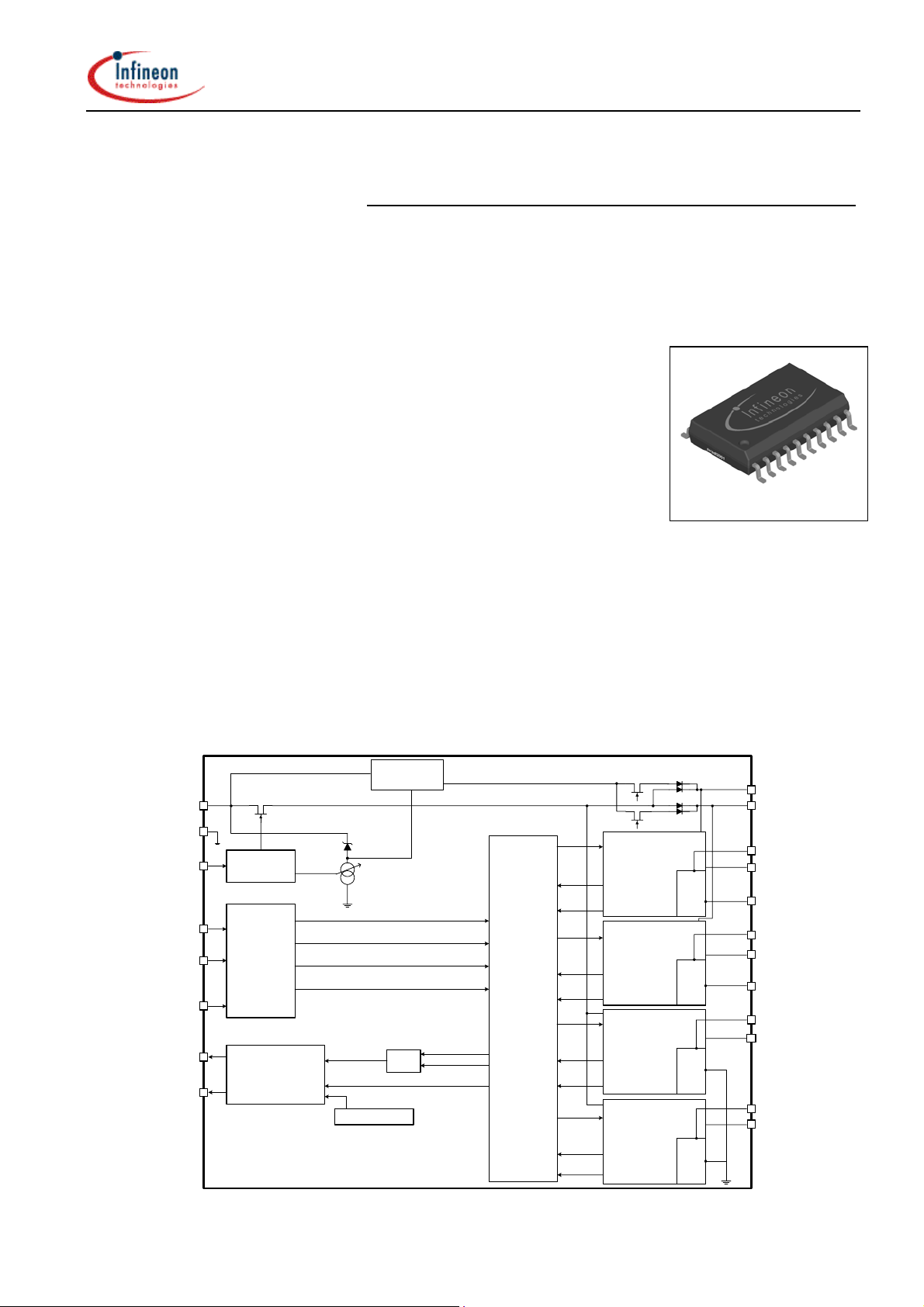
Block Diagram
Charge Pump
OR
Short Cir cuit Detection
Tj > 170oC typ.
Undervoltage HSx
Undervoltage LSx
Level
Shift
Floating HS Dr iver 1
+
limitation HS1
V
GS
+
Short circu it
detect.
+
Undervoltage
Floating HS Dr iver 2
+
V
limitation HS2
GS
+
Short circu it
detect.
+
Undervoltage
Floating LS Dri ver 1
+
V
limitation LS1
GS
+
Short circu it
detect.
+
Undervoltage
Floating LS Dri ver 2
+
V
limitation LS2
GS
+
Short circu it
detect.
+
Undervoltage
BH1
BH2
DH1
GH1
SCD
SH1
DH2
GH2
SCD
SH2
DL1
GL1
SCD
DL2
GL2
SCD
V
S
GND
INH
PWM
DIR
DT/DIS
ER1
ER2
Linear
Regulator
INH
HS1
Input control
Dead time
Undervoltage
Short circuit Detect.
Overtemp. warning
LS1
HS2
LS2
1 2006-01-30

Data Sheet TLE6284G
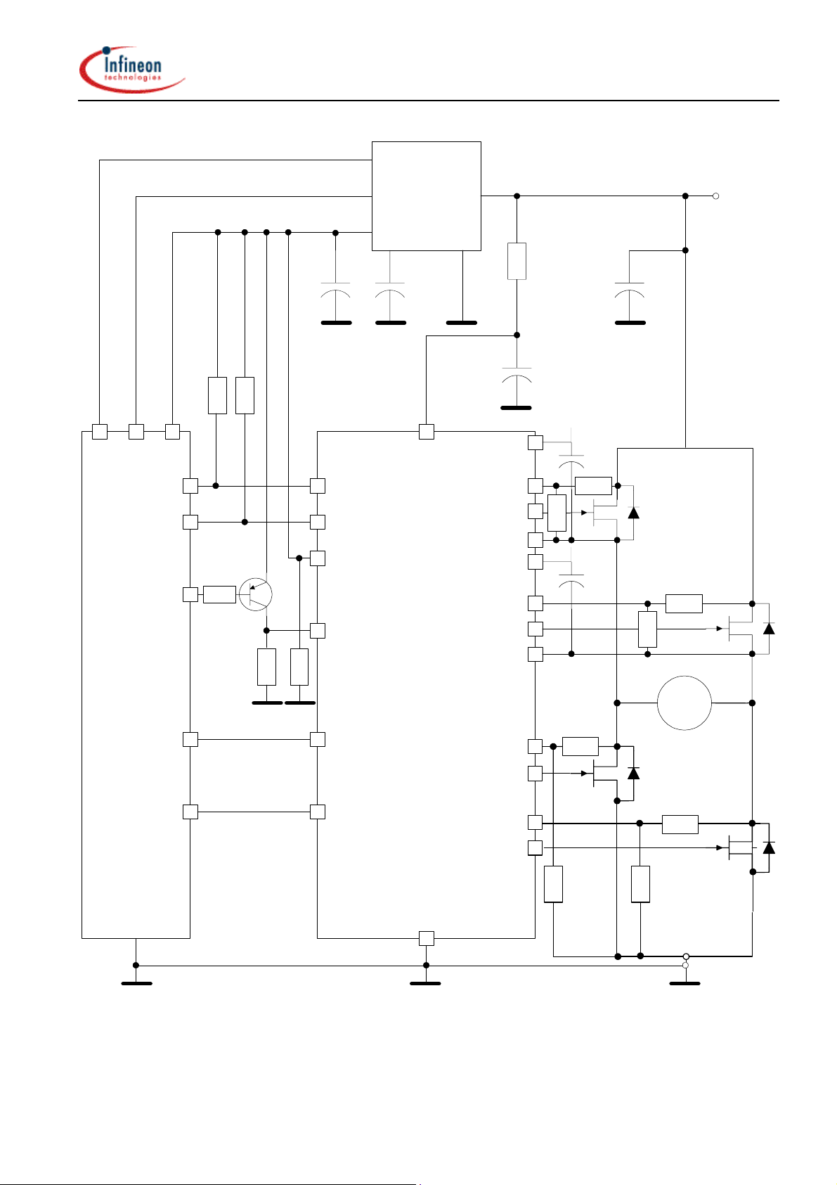
Application Block Diagram
Watchdog
WD R V
µC
R
Q
47kOhm
cc
68 kOhm
10kOhm
R
Q
= 47µF
C
s
R
Q
47kOhm
BCR192W
C
47µF
Q
DT / DIS
R
220k
Reset
Q
ER1
ER2
INH
INH
TLE
4278G
D
= 47nF
C
D
Vs
I
BH1
DH1
GH1
SH1
BH2
DH2
GH2
SH2
R = 10 Ohm
C
s
= 1µF
C
s
R
SCD
= 47µF
C
B
220nF
R
SCD
C
220nF
Vs = 12V
B
R
SCD
R
SCD
M
R
PWM
DL1
GL1
DIR
DL2
GL2
GND
This application block diagram shows one of the possibilities to use this Driver IC. The voltage devider networks accross the 4 MOSFETs (resistors R
limit threshold for Short Circuit protection. The R
the bootstrap capacitors. If R
resistors are not used in the application, a 12k Ohm resistor
SCD
resistors also provide a charge path for
SCD
SCD
should be introduced between SH1 to GND and SH2 to GND.
SCD1
R
SCD3
R
SCD2
R
SCD4
) allow to increas the current
2 2006-01-30

Data Sheet TLE6284G
DT/DIS
ER1
DIR
PWM
DL2
VS
DL1
INH
1
1
2
2
3
3
4
4
5
5
6
6
7
7
8
8
9
9
10
10
TLE6284G
20
20
19
19
18
18
17
17
16
16
15
15
14
14
13
13
12
12
11
11
GL2
SH2
GH2
BH2
DH2
DH1 ER2
BH1 GND
GH1
SH1
GL1
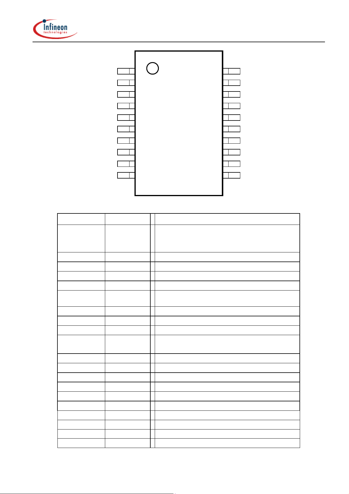
Pin Symbol Function
1 DT / DIS a) Set adjustable dead time by external resistor
b) Reset ERx register
c) Disable output stages
2 ER1 Error flag for driver shut down
3 DIR Control input for spinning direction of the motor
4 PWM Control input for PWM frequency and duty cycle
5 DL2 Sense contact for short circuit detection low side 2
6 ER2 Warning flag Temperature / distinguish if short cir-
cuit or undervoltage lock out occured
7 GND Logic Ground
8 VS Voltage supply
9 DL1 Sense contact for short circuit detection low side 1
10
11 GL1 Output to gate low side switch 1
12 SH1 Connection to source high side switch 1
13 GH1 Output to gate high side switch 1
14 BH1 Bootstrap supply high side switch 1
15 DH1 Sense contact for short circuit detection high side 1
16 DH2 Sense contact for short circuit detection high side 2
17 BH2 Bootstrap supply high side switch 2
18 GH2 Output to gate high side switch 2
19 SH2 Connection to source high side switch 2
20 GL2 Output to gate low side switch 2
INH Sets complete device to sleep mode to achieve low
quiescent currents
3 2006-01-30

Data Sheet TLE6284G
Maximum Ratings at Tj=-40…+150°C unless specified otherwise
Limits ValuesParameter Symbol
Unit
Min. Max.
Supply voltage 1 VS -4 60 V
Operating temperature range
Storage temperature range
Tj
T
stg
-40
-55
150
150
°C
Max. voltage range at PWM, DIR, DT/DIS -1 6V
Max. voltage range at ERx -0.3 6V
Max. voltage range at INH VINH -0.6 60 V
Max. voltage range at BHx VBHx -0.3 90 V
Max. voltage range at DHx
Max. voltage range at GHx
Max. voltage range at SHx
2
VDHx -4 75 V
3
VGHx -6.8 86 V
3
VSHx -6.8 75 V
Max. voltage range at GLx VGLx -2 12 V
Max. voltage range at DLx VDLx -2 75 V
Max. voltage difference BHx – SHx VBHx-VSHx -0.3 17 V
Max. voltage difference Gxx – Sxx VGxx-VSxx -0.3 11 V
Power dissipation (DC) @ TA=125°C / min.footprint P
Power dissipation (DC) @ TA=85°C / min.footprint P
Electrostatic discharge voltage (Human Body Model)
0.33 W
tot
0.85 W
tot
4
V
ESD
2kV
according to MIL STD 883D, method 3015.7 and
EOS/ESD assn. standard S5.1 – 1993
Jedec Level 3
Thermal resistance junction - ambient (minimal foot-
R
75 K/W
thJA
print with thermal vias)
Thermal resistance junction - ambient (6 cm2) R
75 K/W
thJA
Functional range
Parameter and Conditions Symbol Values Unit
at Tj = -40…+150°C, unless otherwise specified
min max
Supply voltage VS 7.5 60 V
Operating temperature range Tj -40 150 °C
Max. voltage range at PWM, DIR, DT/DIS -0.3 5.5 V
Max. voltage range at ERx -0.3 5.5 V
Max. voltage range at INH VINH -0.6 60 V
Max. voltage range at BHx VBHx -0.3 90 V
Max. voltage range at DHx2 VDHx -4 75 V
1
With external resistor (≥10 Ω ) and capacitor
2
The min value -4V is reduced to –( V
3
The min value -7V is reduced to –(V
4
All test involving Gxx pins V
ESD
=1 kV!
BHx
BHx
- V
) in case of bootstrap voltages V
SHx
- V
- 1V) in case of bootstrap voltages V
SHx
BHx-VSHx
BHx-VSHx
<4V
<8V
4 2006-01-30

Data Sheet TLE6284G
Max. voltage range at GHx3 VGHx -6.8 86 V
Max. voltage range at SHx3 VSHx -6.8 75 V
Max. voltage range at GLx VGLx -2 12 V
Max. voltage range at DLx VDLx -2 75 V
Max. voltage difference BHx – SHx VBHx-VSHx -0.3 12 V
Max. voltage difference Gxx – Sxx VGxx-VSxx -0.3 11 V
PWM frequency FPW M 0 50 kHz
Minimum on time external lowside switch – static con-
dition @ 20 kHz; Q
= 200nC
Gate
Electrical Characteristics
Parameter and Conditions Symbol Values Unit
at Tj = -40…150°C, unless otherwise specified
and supply voltage range V
Static Characteristics
S = 7.5 … 60V; f
= 20kHz
PWM
tp(min) 2µs
min typ max
Low level output voltage (VGSxx) @ I=10mA
High level output voltage (VGSxx) @ I=-10mA
Supply current at VS (device disabled)
@ V
= VS =14V R
bat
=400kΩ
DT
Supply current at VS (device disabled)
@ V
= VS =42V R
bat
=400kΩ
DT
Quiescent current at VS (device inhibited)
@ V
R
= VS =14V R
bat
SCD1+RSCD2
DT
= R
SCD3+RSCD4
=400kΩ
=12kΩ
Quiescent current at VS (device inhibited)
@ V
R
Supply current at VS @ V
f
PWM
Supply current at VS @ V
f
PWM
Supply current at VS @ V
f
PWM
= VS =42V R
bat
SCD1+RSCD2
= R
=400kΩ
DT
SCD3+RSCD4
= VS =14V,
bat
= 20kHz (Outputs open)
= VS =14V,
bat
= 50kHz (Outputs open)
= VS =42V,
bat
= 20kHz (Outputs open)
=12kΩ
∆
VLL -- 60 150 mV
∆
VHL 8 10 11 V
IVS(dis)14V -- 4 8 mA
IVS(dis)42V -- 4 8 mA
IVS(inh)14V -- 0.6 1.5 mA
IVS(inh)42V -- 0.6 1.5 mA
I
VS(open)14V
I
VS(open)14V
I
VS(open)42V
-- 7 15 mA
-- 7 15 mA
-- 7 15 mA
Low level input voltage VIN(LL) -- -- 1.0 V
High level input voltage VIN(HL) 2.0 -- -- V
Input hysteresis
Inhibit trip level V
∆
VIN 100 170 mV
1.3 2 3 V
INH
5 2006-01-30
 Loading...