


现货库存、技术资料、百科信息、热点资讯,精彩尽在鼎好!
Datasheet TLE6280GP
3-Phase Bridge Driver IC
Features
•
Compatible to very low ohmic normal
level input N-Channel Mosfets
•
Separate input for each MOSFET
•
PWM frequency up to 30kHz
•
Fulfills specification down to 9V
supply voltage
•
Low EMC sensitivity and emission
•
Separate Source connection for each MOSFET
•
Adjustable dead time
•
Adjustable dI/dt limitation
•
Short circuit protection with adjustable current limitation
•
Driver undervoltage warning
•
Reverse polarity protection
•
Disable function
•
Input with TTL characteristics
•
Error flag
•
Thermal overload warning for driver IC
•
Shoot through protection
•
Shoot through option
•
Integrated bootstrap diodes
Product Summary
Turn on current I
Turn off current I
Supply voltage range V
Gate Voltage VGS 10 V
Temperature range T
0.9 A
Oxx(on)
0.85 A
Oxx(off)
8...20 V
Vs
-40...+150 °C
J
P-DSO36-12
Ordering Code
Q67007-A9406
Application
•
Dedicated for 3-phase high current motor bridges in PWM control mode. This device fulfills requirements in
12V automotive applications
General Description
3-phase bridge driver IC for MOSFET power stages with multiple protection functions.
Block Diagram
BH1 GH1 SH1 BL1 GL1 SL1
HS Driver 1 LS Driver 1
HS Driver (Channel 2)
- Short Circuit Protection
- Undervoltage Detection
-
DI/dt Control
LS Driver (Channel 2)
- Short Circuit Protection
- Undervoltage Detection
-
DI/dt Control
BH2
GH2
BL2
SH2
GL2
VS
ILx
IHx
MFP
DT
ERR
Reverse Polarity
Protection
Input Logic
- Shoot Through Protection
- Shoot Through Option
- Charge Pump Control
- Programmable Dead Time
Error Logic
- Short Circuit Shut Down
- Under Voltage Warning
- Over Temperature Warning
CL
Voltage Regulator
Charge Pump
CH
VDH
DIDT
GND
SL2
DI/dt Limitation
HS Driver 3 LS Driver 3
BH3 GH3 SH3 BL3 GL3 SL3
1 2004-03-31

Datasheet TLE6280GP
Application Block Diagram
VS=12V
R
V5=5V
50 k
VS
10
Ω
C
DI/DT
12nF
C
VS
R
1µF
R
Q
Ω
DI/DT
100
Ω
VS
DI/DT
VDH
P-GND
C
1000µF
V
CC
ERR
R
Q
20 k
Ω
MFP
R
Q
82 k
Ω
BH1
GH1
SH1
BH2
GH2
SH2
BH3
C
BH1
220nF
C
BH2
220nF
C
BH3
220nF
TLE6280GP
GH3
IL1
IH1
µC
C
CP
1.5µF
R
DT
50 k
Ω
IL2
IH2
IL3
IH3
CH
CL
DT
SH3
BL1
GL1
SL1
BL2
GL2
SL2
BH3
GL3
SL3
C
BL1
220nF
C
BL2
220nF
C
BL3
220nF
GND
GND
P-GND
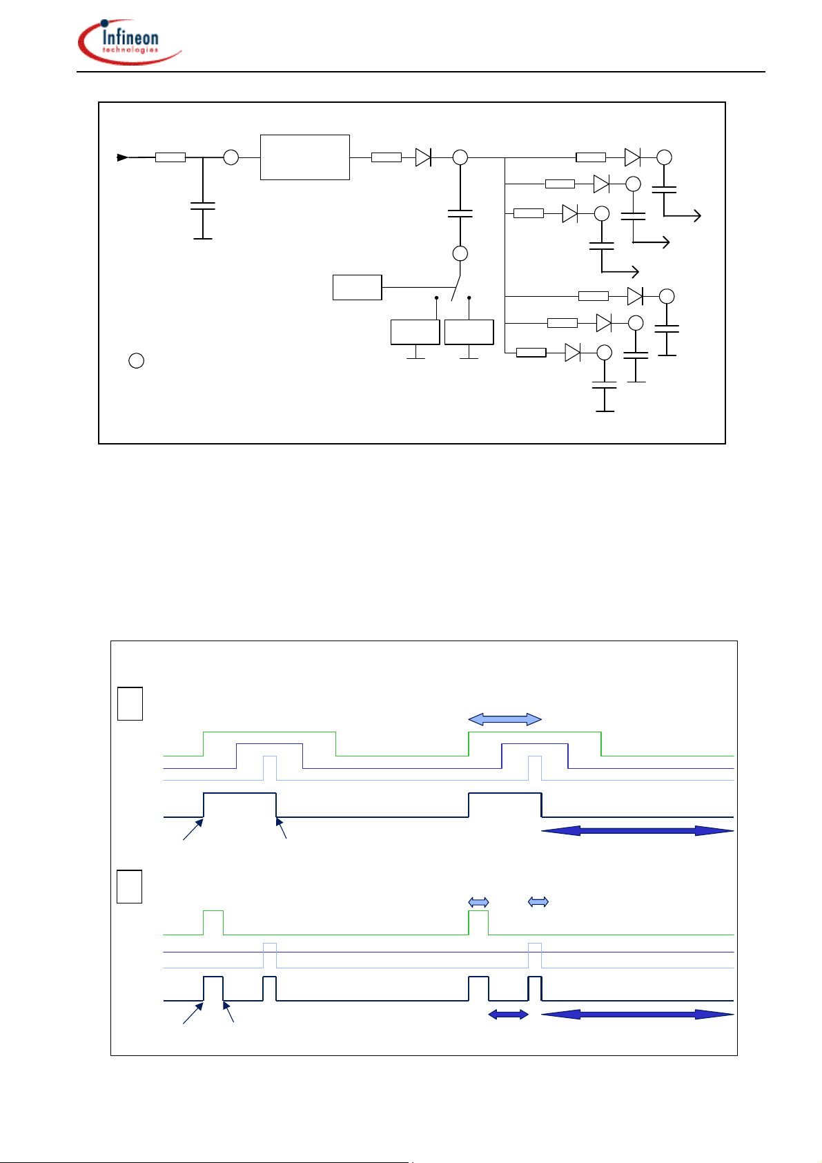
Fig. 1 : Application circuit
Remark: This application diagram is one possible implementation of this driver IC. There is, e.g., the
possibility to link all three BLx pins and use only one capacitor.
2 2004-03-31

Datasheet TLE6280GP
Symbol Function
Pin
1;18;19:36 GND Logic Ground
8 VS Voltage supply
20
21
9
11
13
10
12
14
15 MFP Multi function pin:
17 DT Program pin for dead time
35 DIDT Program pin dI/dt limitation
34 VDH Sense pin for drain voltage of the high-side Mosfets
16 ERR Error flag for driver supply under voltage, over-
2
28
22
5
31
25
3
29
23
6
32
26
4
30
24
7
33
27
CL
CH
IH1
IH2
IH3
IL1
IL2
IL3
BH1
BH2
BH3
BL1
BL2
BL3
GH1
GH2
GH3
GL1
GL2
GL3
SH1
SH2
SH3
SL1
SL2
SL3
Charge pump - capacitor
Control inputs for high-side switches 1 to 3
(low active)
Control inputs for low-side switches 1 to 3
(high active)
a) Disable the complete device by V
MFP
<1V
b) Program pin for output voltage level under short
circuit condition (V
Gxx –VSxx
= 2xV
c) Enable shoot through option by V
MFP
MFP
)
>4.5V
temperature and short circuit (open drain output)
Bootstrap supply high-side switches 1 to 3
Backup capacitor connection low switches 1 to 3
Output to gate high-side switches 1 to 3
Output to gate low-side switches 1 to 3
Connection to source high-side switches 1 to 3
Connection to source low-side switches 1 to 3
3 2004-03-31

Datasheet TLE6280GP
Functional description
General
In the automotive sector there are more and more applications requiring high performance
motor drives, such as electro-hydraulic or electric power steering. In these applications
3-phase motors, synchronous and asynchronous, are used, combining high output performance, low space requirements and high reliability.
The TLE6280GP is a driver IC dedicated to control the 6 to 12 external Mosfets forming the
converter for high current 3 phase motor drives in the automotive sector. It incorporates features like short circuit detection, diagnosis and high output performance and combines it with
typical automotive specific requirements like full functionality even at low battery voltages. Its
3 high-side and 3 low-side output stages are powerful enough to drive Mosfets with 250nC
gate charge with approx. 300ns fall and rise times.
Typical applications are cooling fan, water pump, electro-hydraulic and electric power steering. The TLE6280GP is designed for a 12V power net.
Use in 24V application is possible as well. Limiting factor could be the power dissipation.
This datasheet describes all functionality of this device. Additional application tips are given
in an application note available on the Internet.
Output stages
The 3 low-side and 3 high-side powerful push-pull output stages are all floating blocks, each
with its own Source pin. This allows the direct connection of the output stage to the Source
of each single Mosfet, allowing a perfect control of each Gate-Source voltage even when
200A are driven in the bridge with rise and fall times clearly below 1µs.
All 6 output stages have the same output power and, due to the use of the bootstrap principle, they can be switched all up to 30kHz.
Its output stages are powerful enough to drive Mosfets with 250nC gate charge with approx.
300ns fall and rise times, or even to run 12 such Mosfets with fall and rise times of approx.
600ns.
Maximum allowed power dissipation and the need to refresh the bootstrap capacitors with a
minimum refresh pulse limit the divice use for higher frequencies.
Fig. 2 shows the supply structure of TLE6280GP. The bootstrap capacitors are charged by
the charge pump capacitor C
The exact value for this minimum refresh pulse is given by the RC time constant formed by
the impedance between the CH pin and Bxx pin, and the capacitor formed by the external
Mosfet (C
Mosfet=QGate-total
/ VGS). The size of the bootstrap capacitor has to be adapted to the
external Mosfet that the driver IC has to drive. Usually the bootstrap capacitor is about 10-20
times bigger than C
. External components, such as R-C networks, at the Vs Pin have to
Mosfet
be considered, too.
Operation at Vs<12V – integrated charge pump
The TLE6280GP provides a feature tailored to the requirements of 12V automotive applications. Often the operation of an application has to be assured even at 9V-supply voltage or
lower. Normally bridge driver ICs provide in such conditions clearly less than 9V to the Gate
of the external Mosfet, increasing its RDSon and associated the power dissipation.
The supply structure of the device is shown in fig.2. The TLE 6280GP has a built-in voltage
regulator with charge pump control to generate an internal supply voltage of 13V within a
supply voltage range of 8-40V. Operation below 8V is possible as well and will result in a reduced Gate voltage. The charge pump works with an external capacitor C
tween the CL and CH pins. It provides more than 13V at the CH pin and guarantees high
supply voltage for the bootstrap capacitors C
The Input Low-side pins ILx (see Fig. 3) trigger the charge pump. As soon as the first external low-side Mosfet is switched on and the corresponding bootstrap capacitor is connected
to GND, the CCP is pushed to high and provides about 13V at the CH pin. CCP can now di-
via the CH pin and diodes.
CP
.
Bx
connected be-
CP
4 2004-03-31
from battery
Datasheet TLE6280GP
R
VS
C
VS
VS
Vreg1 13V
+13 ... +8V
CH
C
CP
BH
3
BH
1
BH
2
C
BH1
Phase A
Phase C
BL
2
Phase B
BL
1
C
BL1
= Pin
Bold
line = external component
Triggered
by ILx
Vreg3 =
Vreg1-8V
CL
Vreg2=6V
BL
3
Fig. 2: Supply structure with external components (compare to Fig. 1)
rectly feed the low-side output stages and recharge the bootstrap capacitors connected to
GND.
As soon as the first of the 3 external low-side Mosfets is switched off, the CCP will be pulled
down to be re-charged.
This synchronous operation with the output stages has the benefit that the electromagnetic
emissions generated by the charge pump can be filtered by the same filter necessary to filter
the EME of the converter itself. At the same time it is assured that the high voltage at the CH
pin is available just in time to charge the high-side bootstrap.
! Timing of charge pump - Examples
1
IL1
IL2
IL3
CH
1. ILx high 1. ILx low
2
IL1
IL2
IL3
CH
1. ILx high
1. ILx low
Charge of bootstrap
capacitors
Charge of charge pump
capacitor
Charge of bootstrap capacitors
Charge of charge pump capacitor
Fig. 3: Trigger timing of charge pump caused by changing input signals
5 2004-03-31

Datasheet TLE6280GP
The size of the C
(See “output stages”). CCP is usually 6 times larger then C
and CCP capacitors depends upon the gate charge of the Mosfet.
Bxx
.
Bxx
Dead Time and Shoot through option.
In bridge applications it has to be assured that the external high-side and low-side Mosfets
are not “on” at the same time, such that the battery voltage is directly connected to GND.
This is usually assured by the integration of delays in a driver IC, generating a so-called
dead time between switching off the external Mosfet and switching on the other Mosfet of the
same half-bridge.
The dead times generated in the TLE6280GP are adjustable. The dead time generated by
the TLE6280GP can be varied from 100ns to 4µs by connecting an external resistor from the
DT pin to GND. The dead time has to be long enough to avoid a short between battery and
GND, while the dead time should be as short as possible to reduce extra power dissipation
in the external Mosfets.
In addition to this adjustable delay, the TLE6280GP provides a locking mechanism, preventing both external Mosfets of one half-bridge from being switched on at the same time. This
functionality is called shoot through protection.
If the command to switch on both high and low-side switches in the same half-bridge is given
at the input pins, the command will be ignored. (See dead time diagrams, fig. 6-8)
This shoot through protection can be deactivated by setting the MFP-pin to 5V.
Short circuit protection / current limitation
The TLE6280GP provides a short circuit protection for the external Mosfets, by monitoring
the Drain-Source voltage of the external Mosfets. As soon as this voltage is higher than the
short circuit detection limit, the Gate-Source voltage of this Mosfet will be limited to twice the
voltage at the MFP-Pin, providing a current limitation.
The short circuit detection level is dependent upon the voltage of the MFP pin as well (see
diagrams).
After a delay of about 11µs all external Mosfets will be switched off until the driver is reset by
the MFP pin. The error flag is set.
The Drain-Source voltage monitoring of the short circuit detection for certain external Mosfets is active as soon as the corresponding input is set to “on” and the dead time is expired.
This feature provides a 2-step switch-on behavior for each regular switching-on of a Mosfet.
Description of MFP pin (Multi functional pin)
The MFP pin has multiple tasks:
1) Reset the device.
2) Adjust the short circuit detection level of the external Mosfet and define the gate voltage
limitation for current limitation in case of short circuit
3) Deactivate the shoot-through protection
Fig 4. shows the internal structure of the MFP pin.
Condition of MFP pin Function
0 – 1.1V Disable the driver. All external Mosfets will be actively
switched off
2.5 – 4.0 V Adjustable short circuit detection level combined with adjust-
able gate voltage limitation for current limitation. Shootthrough protection is active.
> 4.5V Shoot-through protection deactivated.
6 2004-03-31

Datasheet TLE6280GP
&
ILx
NAND
IHx
4.5V
MFP
Vmfp x 2
1.45 /
1.7V
Fig. 4: Block diagram of internal structure of MFP pin
80ns
&
Levelshifter
Shoot
Through
Gate
control
Dissable
=
Reset
Shoot through protection / option
As already mentioned, the device has a built-in shoot-through protection, to avoid a simulta-
neous activation of high- and low-side switch in one half-bridge.
In case there is a short circuit in the bridge, the driver will switch off all external Mosfets. If
there is still current flowing in the motor, it is possible for the user to override this shoot
through protection.
By setting the ILx to “high”, the IHx to “low” and MFP to a level above 4.5V, all external Mosfets will be turned on simultaneously to blow a well-dimensioned fuse. The application will be
finally disconnected in this way from battery, and thus guarantee that the motor does not apply any uncontrolled torque.
Undervoltage warning:
If the voltage of a bootstrap capacitor C
reaches the undervoltage warning level the error
Bxx
flag is set and will remain set until the voltage of the bootstrap capacitor has recovered.
The error signal can be seen as awarning that an undervoltage shut-down could occur soon,
and the user can take appropriate measures to avoid this. Such measures could be the
change of the duty cycle to a range of 10-90% or the ramp down of the motor.
Undervoltage shut down:
The TLE6280GP has an integrated undervoltage shut-down, to guarantee that the behavior
of the device is predictable in all voltage ranges.
If the voltage of a bootstrap capacitor C
reaches the undervoltage shut-down level, the
Bxx
Gate-Source voltage of the affected external Mosfet will be actively pulled to low. In this
situation the short circuit detection of this output stage is deactivated to avoid a complete
shut down of the driver. This allows continued operation of the motor in case of undervoltage
shut-down for a short period of time.
7 2004-03-31
Datasheet TLE6280GP
As soon as the bootstrap voltage recovers, the output stage condition will be aligned to the
input patterns by the next changing input signal at the corresponding input pin.
Diagnosis
The ERR pin is an open collector output and has to be pulled up with external pull-up resis-
tors to 5V. In normal conditions the ERR signal is high. In case of an error the ERR pin is
pulled down. There are 3 different causes for an error signal:
1) Short circuit of an external Mosfet – all external Mosfets are switched off. The driver has
to be reset to start again.
2) Undervoltage warning: at least one of the external capacitors connected to Bxx pins has
a voltage below the warning level.
3) Over-temperature warning: The device works normally but is out of the maximum ratings.
Immediate actions have to be taken to reduce the thermal load. The error flag will be removed when the driver reached temperatures below the over temperature warning level.
Temperature
Sensor
ERR
I undervoltage
τ approx. 1µs
Iscp (VMFP)
3.3µA
0.3µA
Fig. 5: Block diagram of ERR functionality
10pF
OR
dI/dt control
In all high current PWM applications, transient overvoltages and electro-magnetic emmisions
are critical items. The dI/dt regulation of the TLE6280GP helps to reduce transient overvoltage as well as electro-magnetic emissions.
Each real bridge configuration has stray inductance in each half-bridge. When the Mosfets in
the bridge are switching and load current is flowing, the stray inductance together with the
dI/dt in the halfbridge causies transient overvoltages. These transient overvoltages can be
feed to the DIDT pin of the gate driver by a high pass filter. Voltages exceeding 2 to 5V or –2
to –5V at this pin will strongly reduce the gate current of the actually switched Mosfet, resulting in an increased switching time in the Miller plateau of the Mosfet, and reducing the
switching speed exactly and only in the critical area of the switching process. Through this
regulation over-voltages are reduced and a smoother dI/dt in the bridge is obtained.
For more detailed information please refer to application note.
Estimation of power dissipation within the driver IC
8 2004-03-31

Datasheet TLE6280GP
The power dissipation within the driver IC is strongly dependent upon the use of the driver
and the external components. Nevertheless, a rough estimation of the worst case power dissipation is possible.
Worst case calculation is:
PD = (Q
With:
PD = Power dissipation in the driver IC
f
= Switching frequency
PWM
Q
= Total gate charge of used MOSFET at 10V VGS
gate
n = number of switched Mosfets
const = constant considering some leakage current in the driver and the power dissipa-
I
VS(open)
VVS = Voltage at Vs
P
RGate
This value can be reduced dramatically by the use of external gate resistors.
Recommended start up procedure
To assure the driver to be active and functional, a special initialization procedure is required
whenever the gate drive is enabled (V
enabled, after 10µs or later, positive-going transition signals at all ILx pins are required in order to ensure proper start-up of the output driver. This procedure assures a proper wake up
the device and allowes to fill the bootstrap capacitors. Not filling the bootstrap capacitors
might lead to low Gate-Source voltages mainly in highside and can cause a short circuit detection when the highside switches are activated. Not changing the ILx input signal after
enabling the device may cause the lowside outputs to stay in off conditions.
*n*const* f
gate
PWM
+ I
VS(open)
) * VVs - P
RGate
tion caused by the charge pump (nominally = 2)
= Current consumption of driver without connected Mosfets during switching
= Power dissipation in the external gate resistors
is changed from LO to HI). Every time the driver is
MFP
9 2004-03-31

Datasheet TLE6280GP
Maximum ratings
Parameter and Conditions Symbol Values Unit
at Tj = -40 … +150 °C, unless otherwise specified
Supply voltage
Operating temperature range
Storage temperature range
Max. voltage range at Ixx, MFP, DT; ERR -0.3 ...+7 V
Max. voltage range at SLx2 VSLx -7 ...+7 V
Max. voltage range at SHx3 VSHx -7 ...+45 V
Max. voltage range at GLx2
Max. voltage range at GHx3
Max. voltage range at BHx3
Max. voltage range at VDH4
Max. voltage difference Bxx - Sxx VBxx-VSxx -0.3 ...+15 V
Max. voltage difference Gxx - Sxx VGxx-VSxx -0.3...+11 V
Max. voltage range at CL VCL -0.3 ...+10 V
Max. voltage range at CH VCH -0.3 ...+18 V
Max. voltage range at DIDT VDIDT -7 ...+7 V
Power dissipation (DC) @ TC=125°C P
ESD voltage (Human Body Model)
JESD22-A114-B
@ all pins
@ all pins excluding Gxx
DIN humidity category, DIN 40 040 E
IEC climatic category, DIN IEC 68-1 40/150/56
Jedec Level 3
Thermal resistance junction-case R
1
VS -4 ... 45V V
Tj
T
stg
-40 ...+150
-55 ...+150
VGLx
-7 ...+18
VGHx
-7 ...+55
VBHx
-0.3 ...+55
VVDH
-4 ...+55
1.2 W
tot
V
ESD
1
2
≤5K/W
thJC
°C
V
V
V
V
kV
1
With external resistor (≥10 Ω ) and capacitor – see fig.1
2
The min value -7V is reduced to –(Vs - 0.5V) if Vs<7.5V
3
The min value -7V is reduced to –(V
4
The min value -4V is increased to –( V
BHx-VSHx
-1V) if bootstrap voltages <8V
- V
BHx
) if bootstrap voltages <4V
SHx
10 2004-03-31

Datasheet TLE6280GP
Functional range
Parameter and Conditions Symbol Values Unit
at Tj = -40 … +150 °C, unless otherwise specified
Supply voltage
Operating temperature range Tj -40 ...+150 °C
Duty Cycle @ 20kHz
Max. voltage range at Ixx, ERR VIxx; VERR -0.3 ...+7 V
Max. voltage range at MFP, DT9 VMFP -0.3 ...+5 V
Max. voltage range at SLx2 VSLx -7 ...+7 V
Max. voltage range at SHx3 VSHx -7 ...+45 V
Max. voltage range at GLx2 VGLx -7 ...+18 V
Max. voltage range at GHx3 VGHx -7 ...+55 V
Max. voltage range at BHx3 VBHx -0.3 ...+55 V
Max. voltage range at VDH4 VVDH -4 ...+55 V
Max. voltage difference Bxx - Sxx VBxx-VSxx -0.3 ...+15 V
Max. voltage difference Gxx - Sxx VGxx-VSxx -0.3...+11 V
Max. voltage range at DIDT VDIDT -7 ...+7 V
PWM frequency10 FPWM 2...50 kHz
Min. dead time resistor RDT 0kΩ
567
VS 8 ... 20 V
678
Vs>8V dc 0...95 %
5
operation above 20V limited by max allowed power dissipation and max. ratings
6
If all 3 half-bridges are switched with f
Vs=9.5V
7
Total gate charge of the attached Mosfet < 250nC
8
If the bootstrap capacitor is charged to V
9
V
up to 7V allowed up to 500ms
MFP
10
Limited only by the minimum bootstrap voltage (undervoltage logout of output stage) and the max allowed
power dissipation
and a duty cycle <10%, undervoltage shut down can occur below
PWM
BHx-VSHx
=12V, the maximum duty cycle is 100% for 500 µs
11 2004-03-31

Datasheet TLE6280GP
Electrical Characteristics
Parameter and Conditions Symbol Values Unit
at Tj = –40 … +150 °C, unless otherwise specified
and supply voltage range V
S = 8 ... 20V; f
= 20kHz
PWM
Static Characteristics
min typ max
Low level output voltage (VGxx-VSxx) @ I=10mA
High level output voltage (VGxx-VSxx) 7
∆
VLL -- 50 100 mV
∆
VHL 8 10 11 V
@ I=-10mA
Supply current at VS (device disabled)
@ V
bat=VS
Supply current at VS @ 20kHz V
=14V RDT=400kΩ V
MFP
=0V
MFP
≤4V
IVS(dis) -- -- 12 mA
I
VS(open)
-- 19 28 mΑ
(Outputs open)
Low level input voltage VIN(LL) -- -- 1.0 V
High level input voltage VIN(HL) 2.0 -- -- V
Input hysteresis
∆
VIN 200 mV
Dynamic characteristics
Turn on current @ V
@ VGxx -VSxx = 4V; Tj=125°C
Turn off current @ VGxx -VSxx = 10V; Tj=25°C
@ VGxx -VSxx = 4V; Tj=125°C
Dead time (adjustable) @ RDT = 10 kΩ
@ RDT = 50 kΩ
@ R
@ R
@ RDT > 1 MΩ
Dead time @ RDT = 0 kΩ
@ TJ = -40°C
@ T
= +25°C
J
@ TJ = +150°C
Rise time @ C
V
CLoad
Load
@ TJ = -40°C
@ TJ = +25°C
@ TJ = +150°C
Fall time @ C
V
@ T
@ TJ = -40°C
CLoad
= +25°C
J
Load
@ TJ = +150°C
Gxx -VSxx = 0V; T
=22nF; R
=22nF; R
Load
Load
=25°C
j
DT = 200 kΩ
DT = 400 kΩ
=1Ω; 20…80%
=1Ω; 20…80%
IGxx(on) --
IOxx(off) --
tDT 0.16
t
DT
20
25
45
t
rise
fall
t
--
--
--
--
--
--
--
--
--
--
--
--
0.93
0.95
0.85
0.55
0.25
1.2
3.9
4.1
2.2
55
70
110
310
250
170
220
250
200
0.35
125
130
200
700
600
600
400
350
350
--
Α
--
--
Α
-µs
--
--
--
-ns
ns
ns
12 2004-03-31

Datasheet TLE6280GP
Electrical Characteristics (continued)
Parameter and Conditions Symbol Values Unit
at Tj = –40 … +150 °C, unless otherwise specified
and supply voltage range V
S = 8 ... 20V; f
= 20kHz
PWM
Dynamic characteristics (continued)
Disable propagation time t
Wake up time after enabling the device tWU 10 µs
Input propagation time (low on) tP(ILN) -- 220 500 ns
Input propagation time (low off) tP(ILF) -- 180 500 ns
Input propagation time (high on) tP(IHN) -- 250 500 ns
Input propagation time (high off) tP(IHF) -- 185 500 ns
Input propagation time difference
(all channels turn on)
Input propagation time difference
(all channels turn off)
Input propagation time difference
(one channel; high off – low on)
Input propagation time difference
(one channel; low off – high on)
Input propagation time difference
(all channels; high off – low on)
Input propagation time difference
(all channels; low off – high on)
DC-Resistance between CH and Bxx pin
I
CH-Bxx
= 50mA; V
VS
= V
= GND = 0V
Bxx
@ TJ = -40°C
@ TJ = +25°C
@ TJ = +150°C
Boostrap diode forward voltage I
CH-Bxx
= 50mA
@ TJ = -40°C
@ TJ = +25°C
@ TJ = +150°C
min typ max
P(DIS) -- 350 700 ns
tPD(an) 20 55 70 ns
tPD(af) -- 11 50 ns
tPD(1hfln) -- 60 150 ns
tPD(1lfhn) -- 80 150 ns
tPD(ahfln) -- 60 150 ns
tPD(alfhn) -- 80 150 ns
RCH-Bxx --
Ω
3.3
4.2
6.0
V
BSD --
0.84
0.73
0.52
6.3
7.3
8.3
V
1.2
1.0
0.76
13 2004-03-31
Datasheet TLE6280GP
Electrical Characteristics (continued)
Parameter and Conditions Symbol Values Unit
at Tj = –40 … +150 °C, unless otherwise specified
and supply voltage range V
V
>7.5V
Bxx
S = 8 ... 20V; f
= 20kHz;
PWM
Diagnosis and Protection Functions
Undervoltage warning at ERR
@ T
= -40°C
J
@ T
= +25°C
J
@ TJ = +150°C
Undervoltage shut down of output stage
@ T
= -40°C
J
@ TJ = +25°C
@ TJ = +150°C
Over-temperature warning11 T
Hysteresis for over-temperature warning ∆T
Short circuit protection shut down time delay t
Short circuit criteria (VDS of Mosfets) @
V
=3V12
MFP
@ TJ = -40°C
@ TJ = +25°C
@ TJ = +150°C
Factor between V
@ 2V < V
MFP
< 4V
and max. V
MFP
GXX
Disable input level V
Enable input level 13 V
Disable input hysteresis ∆V
Error level @ 1.6mA I
V
ERR
V
Bxx-VSxx
V
Bxx-VSxx
J(OV)
SCP(off)
V
DS(SCP)
V
GxxMax/VMFP
MFP(DIS)
MFP(EN)
ERR
150 170 190 °C
20 °C
J(OV)
7 11 15 µs
-- -- 1.1 V
2.5 -- -- V
MFP(DIS)
-- 500 -- mV
-- -- 1.0 V
min typ max
8
8
8
9.4
9.3
9.0
5.5
5.0
4.0
7.2
6.6
5.6
1.4
--
--
1.85
1.90
1.95
1.67 2 2.27
V
10
10
10
V
7.5
7.2
7.2
V
--
--
2.3
Shoot through option
Shoot through protection activated V
MFP 4V
Shoot through option activated VMFP 4.5 -- -- V
11
specified by design
12
Periodic short circuit condition will be detected within several cycles, if the duty cycle is more than 10%
13
If the device is enabled, the slope of dU
/dt has to be higher than 3.5V/50µs
(VMFP)
14 2004-03-31

Datasheet TLE6280GP
Electrical Characteristics (continued)
Parameter and Conditions Symbol Values Unit
at Tj = –40 … +150 °C, unless otherwise specified
and supply voltage range V
V
>7.5V
Bxx
S = 8 ... 20V; f
= 20kHz;
PWM
dI /dt limitation
Non reaction level for dI/dt limitation (100% gate
driver capability) @ V
DIDT
>0V
Non reaction level for dI/dt limitation (100% gate
driver capability) @ V
Max. V
V
DIDT
at full reaction level for dI/dt limitation @
Gxx
= -5V
DIDT
<0V
@ TJ = -40°C
@ TJ = +25°C
@ TJ = +150°C
Min. falltime at full reaction level for dI/dt limitation
@ V
DIDT
= +5V
@ TJ = -40°C
@ TJ = +25°C
@ TJ = +150°C
Impedance of DIDT Pin to GND
10kHz<f<10MHz; V
DIDT
= 5V
Default status of input pins:
To assure a defined status of all input pins in case of disconnection, these pins are internally
secured by pull-up or pull-down current sources with approx. 10µA.
The following table shows the default status of each input pin.
Input pin Default status
ILx Low (ext. Mosfet off)
IHx High (ext. Mosfet off)
DIDT Low (no dI/dt limitation)
DT 2µs dead time
MFP Disable (pull-down)
min typ max
VDIDT 2 -- -- V
VDIDT -- -- -2 V
1.9
2.3
3.4
65
68
70
3.0
3.0
4.2
--
--
--
VGxx(DIDT)
--
--
--
t
fall (DIDT)
20
20
20
ZDIDT 60 Ω
V
µs
15 2004-03-31

Datasheet TLE6280GP
Truth Table
Input Conditions Output
ILx IHx DT MFP UV OT SC GLx GHx ERR
1 1 D >2.5V 0 0 0 1 0 5V
0 0 D >2.5V 0 0 0 0 1 5V
1 0 D 2.5-4.0V 0 0 0 A A 5V
0 1 D >2.5V 0 0 0 0 0 5V
0 0 D >2.5V 1 0 0 0 1 0V
1 1 D >2.5V 1 0 0 1 0 0V
1 0 D 2.5-4.0V 1 0 0 A A 0V
0 1 D >2.5V 1 0 0 0 0 0V
0 0 D >2.5V 0 1 0 0 1 0V
1 1 D >2.5V 0 1 0 1 0 0V
1 0 D 2.5-4.0V 0 1 0 A A 0V
0 1 D >2.5V 0 1 0 0 0 0V
X X D >2.5V 0 0 1 0 0 B
X X D <1.1V 0 0 X 0 0 5V
X X D <1.1V 1 0 X 0 0 0V
X X D <1.1V 0 1 X 0 0 0V
X X D <1.1V 1 1 X 0 0 0V
C C D >4.5V X X X 1 1 0V
A) stays in the output condition prior to the shoot through input command (see also dead
time diagrams)
B) ERR=0V and stays latched until reset
C) All 3 ILx=1 AND all 3 IHx=0 (shoot through command)
D) No influence on static results
X) Can be 0 or 1
Remark:
If 1.1V < VMFP < 2.5V the device is either working normally or is disabled.
If 4.0V < VMFP < 4.5V the device is either working normally or will allow shoot through.
Definition:
In this datasheet a duty cycle of 98% means that the GLx pin is 2% of the PWM period in
high condition.
Remark: Please consider the influence of the dead time for your input duty cycle
16 2004-03-31
Datasheet TLE6280GP
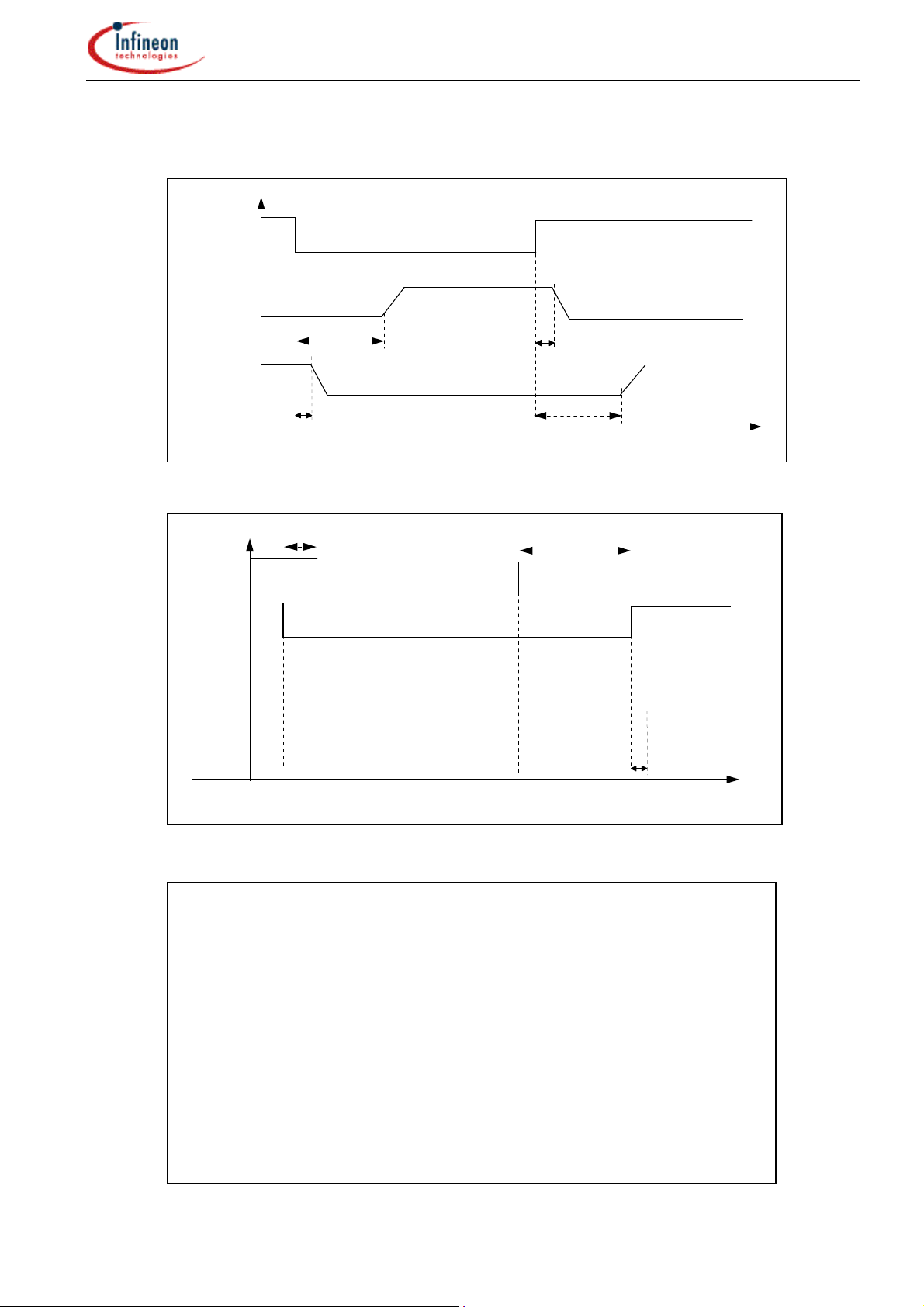
Dead time diagrams:
ILx+IHx
GHx
tDT + tP(IHN)
90%VGHx
10%VGHx
tP(IHF)
GLx
Fig. 6: Dead time generation when IHx and ILx are tied together
90%VGLx
10%VGLx
tP(ILF) tDT + tP(ILN)
t < tDT t > tDT
IHx
ILx
GHx
tDT + tP(IHN)
tP(IHF)
GLx
tP(ILF) tDT
tP(ILN)
t
t
Fig. 7: Dead time generation when IHx and ILx are seperated
IHx
ILx
GHx
tDT + tP(IHN)
GLx
Fig. 8: Dead time gereration and shoot through prote ction
90%VGLx
tP(ILF) tDT + tP(ILN)
tP(IHF)
17 2004-03-31
t

Datasheet TLE6280GP
Typ. dead time generation
Parameter: T
Junction
5
4,5
4
3,5
3
2,5
2
1,5
1
0,5
0
0 100 200 300 400 500 600 700 800 900 1000
R DT [kOhm]
25°C
150°C
-40°C
Fig. 9: Typ. dead time internal generated
2,5
2
1,5
1
0,5
0
0 102030405060708090100
R DT [kOhm]
Fig. 10: Typ. dead time internal generated - detail
25°C
150°C
-40°C
18 2004-03-31

Datasheet TLE6280GP
p
)
Typ. undervoltage shut down level
7,5
7
6,5
6
5,5
5
-40-200 20406080100120140
Temperature [°C]
Typ. Current consumption of output stage
Conditions: Vs=12V; measured with V(BHx=12V) and potentiometer between SHx and GND
Parameter: MFP voltage / T
Fig. 11: Typ. undervoltage shut down (Voltage of
bootstra
capacitors
Junction
1,8
1,6
1,4
1,2
1
0,8
0,6
0,4
0,2
0
567891011
V(Bxx)-V(Sxx) [V]
Fig. 12: Leakage current of driver output stages measured
as current out of SH Pin to GND
2V 150°C
4V 150°C
5V 150°C
2V 25°C
4V 25°C
5V 25°C
2V -40°C
4V -40°C
5V -40°C
Remark:
The leakage current of the driver output stage is taken from the bootstrap capacitors C
. When an external
BX
high-side Mosfet is switched on, it is impossible to replace this current. The capacitor will be discharged as long
as this Mosfet stays on. The time until this output stage reaches the undervoltage shut-down can be determined
by the size of the capacitor, the initial capacitor voltage, the leakage current taken out of this capacitor and the
undervoltage lock-out level.
19 2004-03-31

Datasheet TLE6280GP
Typ. Boostrap voltage vs. Duty Cycle
Conditions: Mosfet: 6x SPB80N04S2-04; f
Parameter: Charge pump capacitor C
14
12
10
PWM
/ Bootstrap capacitor CBX
CP
=20kHz, Vs=9V
8
6
4
2
0
0 102030405060708090100
Duty Cycle [%]
Fig. 13: Typ. bootstrap voltage V(BHx)-V(SHx);
duty cycle of 1 half-bridge = 50%; duty cycle of the other
2 halfbridges variable
1.5µF / 220nF
3µF / 440nF
4.5µF / 660nF
14
12
10
8
6
1.5µF / 220nF
3µF / 440nF
4.5µF / 660nF
4
2
0
0 102030405060708090100
Duty Cycle [%]
Fig. 14: Typ. bootstrap voltage V(BHx)-V(SHx);
duty cycle of 1 half-bridge = 0%; duty cycle of the other 2
halfbridges variable
Remark:
The reachable duty cycle depends on the used PWM patterns. To achieve an even higher duty cycle, run it for
some periods and reduce the duty cycle only for 1 period down to 90% to recharge the bootstrap capacitors.
20 2004-03-31

Datasheet TLE6280GP
g
Typ. Short circuit detection level
Conditions: Vs=12V
Parameter: T
Typ. Gate voltage limitation during short circuit detection
Conditions: Vs=12V; Load at output: capacitor with 22nF; V(SHx) = GND; V(SLx) = GND;
For HS (high-side output); Short happens during on phase V(VDH)-V(SHx)=3V;
For LS (low-side output); Short happens during on phase V(SHx)-V(SLx)=3V;
Parameter: T
Junction
3
2,8
2,6
2,4
2,2
2
1,8
1,6
1,4
Short circuit detection level [V]
1,2
1
2,533,544,55
MFP voltage [V]
Fig. 15: Short circuit detection level
; high-side (HS) or low-side (LS) output
Junction
2,20
+150°C
+25°C
-40°C
2,15
2,10
2,05
2,00
1,95
1,90
1,85
1,80
2 2,2 2,4 2,6 2,8 3 3,2 3,4 3,6 3,8 4
V(MFP) [V]
HS 150°C
HS 25°C
HS -40°C
LS 150°C
LS 25°C
LS -40°C
Fig. 16: Factor between reduced gate voltage V(Gxx) in
case of short circuit and the volta
e at the MFP pin
21 2004-03-31

Datasheet TLE6280GP
)
)
Typ. Switching behavior
Conditions: Vs=12V; Vbb=12V; I
one SPB80N04 S2-04 per output with Q
20
18
16
14
12
10
8
6
4
2
0
0 0,10,20,30,40,50,60,70,80,9 1
Load
= 10A; V
= 135nC; Measured: V(DS)
G(total)
MFP
time [µs]
=3.75V; R
=1Ω; RDT=10kΩ; C
Gate
V(GS)
V(DS
=220nF; CCP=1,5µF;
Bxx
Fig. 17: typ. fall-time at 25°C
14
12
10
8
6
4
2
0
00,20,40,60,811,21,4
time [µs]
Fig. 18: typ. rise-time at 25°C
180
160
140
120
100
80
60
40
20
0
-40-200 20406080100120140
Temperature Tj [°C]
V(GS)
V(DS
fall time
rise time
Fig. 19: Rise- and fall-times vs. temperature T
J
22 2004-03-31

Datasheet TLE6280GP
Package and Ordering Code
Package: P-DSO36-12
(all dimensions in mm)
23 2004-03-31

Datasheet TLE6280GP
Published by
Infineon Technologies AG,
Bereich Kommunikation
St.-Martin-Strasse 53,
D-81541 München
© Infineon Technologies AG 1999
All Rights Reserved.
Attention please!
The information herein is given to describe certain components and shall not be considered as warranted characteristics.
Terms of delivery and rights to technical change reserved.
We hereby disclaim any and all warranties, including but not limited to warranties of non-infringement, regarding
circuits, descriptions and charts stated herein.
Infineon Technologies is an approved CECC manufacturer.
Information
For further information on technology, delivery terms and conditions and prices please contact your nearest Infineon Technologies Office in Germany or our Infineon Technologies Representatives worldwide (see address
list).
Warnings
Due to technical requirements components may contain dangerous substances. For information on the types in
question please contact your nearest Infineon Technologies Office.
Infineon Technologies Components may only be used in life-support devices or systems with the express written
approval of Infineon Technologies, if a failure of such components can reasonably be expected to cause the failure of that life-support device or system, or to affect the safety or effectiveness of that device or system. Life
support devices or systems are intended to be implanted in the human body, or to support and/or maintain and
sustain and/or protect human life. If they fail, it is reasonable to assume that the health of the user or other persons may be endangered.
24 2004-03-31
 Loading...