

现货库存、技术资料、百科信息、热点资讯,精彩尽在鼎好!
System Basis Chip TLE 6266 G
Target Datasheet
1Features
• Standard Fault Tolerant differential CAN-Transceiver
• Bus Failure Management
• Low current consumption mode <70µA
• CAN Data Transmission Rate up to 125 kBaud
• Low-Dropout Voltage Regulator 5V ± 2%
• Two Low Side Switches
• Three High Side Switches with internal Charge Pump
• Power On and Under-Voltage Reset Generator
• Vcc Supervisor
• Window Watchdog
• Flash Program Mode
• Programable Cyclic Wake Timing via SPI
• Integrated Fail-Safe Mechanism
• Standard 16 bit SPI-Interface
• Wide Input Voltage and Temperature Range
• Thermal Protection
• Enhanced Power P-DSO-Package
• Wakeup Input Pin
P-DSO-28-6
Enhanced Power
Type Ordering Code Package
TLE 6266 G on request P-DSO-28-6
2 Description
The TLE 6266 G is a monolithic integrated circuit in an enhanced power P-DSO-28-6
package, which incorporates a failure tolerant low speed CAN-transceiver for differential
mode data transmission, a low dropout voltage regulator for internal and external 5V
supply as well as a 16 bit SPI interface to control and monitor the IC. Further there are
integrated additional features like three high side switches, two low side switches, a
window watchdog circuit and a reset circuit. The IC offers a low current consumption
mode, that reduces the current to typ. 70µA.
The IC is designed to withstand the severe conditions of automotive applications and is
optimized for low-speed data transmission (up to 125 kBaud).
Version 1.06 2 2002-11-26
3 Pin Configuration
(top view)
Target Datasheet TLE 6266
CANH
CANL
OUTH1
1
2
RTH
3
RO
4
5
RTL
6
GND GND
7
GND
8
GND GND
9
GND
10
28
27
26
25
24
23
22
21
20
19
WK
PWM
TxD
RxD
Vcc
GND
GND
CLK
OUTL1
OUTL2
OUTH2
OUTH3
11
12
13
14
(enhanced power package)
Figure 1 TLE 6266 Block Diagram
P-DSO-28-6
18
17
16
15
DI
DO
CSN
Vs
Version 1.06 3 2002-11-26
Target Datasheet TLE 6266
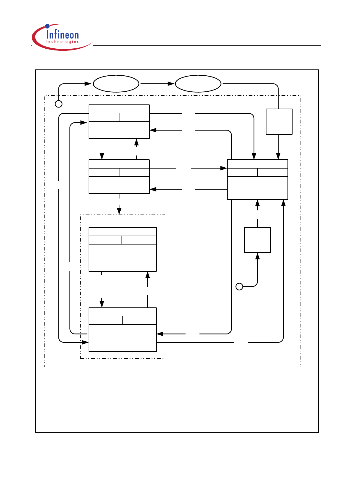
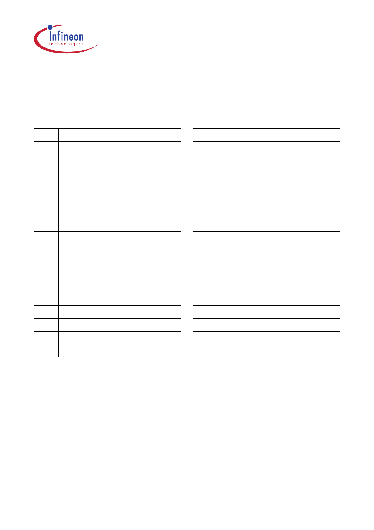
4 Pin Definitions and Functions
Pin No. Symbol Function
1CANHCAN-H bus line; HIGH in dominant state
2RTHCANH-Termination input; connected to CANH via external
termination resistor
3ROReset output; open drain output; integrated pull up; active LOW
4CANLCAN-L bus line; LOW in dominant state
5RTLCANL-Termination input; connected to CANL via external
termination resistor
6, 7, 8, 9,
20, 21,
GND Ground; to reduce thermal resistance place cooling areas on
PCB close to this pins.
22, 23
10 OUTH1 High side output 1; controlled via PWM input and/or SPI input,
short circuit protected
11 OUTL1 Low side output 1; SPI controlled, with active zener
12 OUTL2 Low side output 2; SPI controlled, with active zener
13 OUTH2 High side output 2; SPI controlled
14 OUTH3 High side output 3; SPI controlled, in cyclic wake mode
controlled by an internal autotiming function
15
VS Power supply; block to GND directly at the IC with ceramic
capacitor
16 CSN SPI interface Chip Select Not; CSN is an active low input; serial
communication is enabled by pulling the CSN terminal LOW.
CSN input should only be transitioned when CLK is LOW. CSN
has an internal active pull up and requires CMOS logic level
inputs. See Figure 11 for more details.
17 DO SPI interface Data Out; DO is a tristate output that transfers
diagnosis data to the control device. Serial data transfered from
DO is a 16 bit diagnosis word with the Least Significant Bit (LSB)
transmitted first. The output will remain 3-stated unless the device
is selected by a LOW on Chip-Select-Not (CSN). DO will accept
data on the rising edge of CLK-signal; see Table 6 for output data
protocol and Figure 11 for more timing details.
Version 1.06 4 2002-11-26

Target Datasheet TLE 6266
4 Pin Definitions and Functions (cont’d)
Pin No. Symbol Function
18 DI SPI interface Data In; DI receives serial data from the control
device. Serial data transmitted to DI is a 16 bit control word with
the Least Significant Bit (LSB) transferred first. The input has an
active pull down and requires CMOS logic level inputs. DI will
accept data on the falling edge of CLK-signal; see Table 6 for
input data protocol and Figure 11 for more details.
19 CLK SPI interface clock input; clocks the shiftregister; CLK has an
internal active pull down and requires CMOS logic level inputs
24 V
CC
Output voltage regulator; 5V logic supply, block to GND with an
100nF external ceramic capacitor directly at the IC + external
capacitor C
³ 22 µF
Q
25 RxD CAN Receive data output; push-pull output;
LOW: bus becomes dominant, HIGH: bus becomes recessive
26 TxD CAN Transmit data input; integrated pull up;
LOW: bus becomes dominant, HIGH: bus becomes recessive
27 PWM Pulse Width Modulation control; integrated pull down, active
HIGH. To PWM-control highside-switch HS1
28 WK Wake-Up input; for detection of external wake-up events within
cyclic wake mode, integrated pull down, active HIGH, switches on
rising edge
Version 1.06 5 2002-11-26
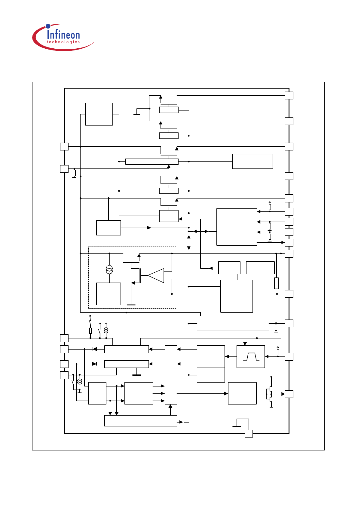
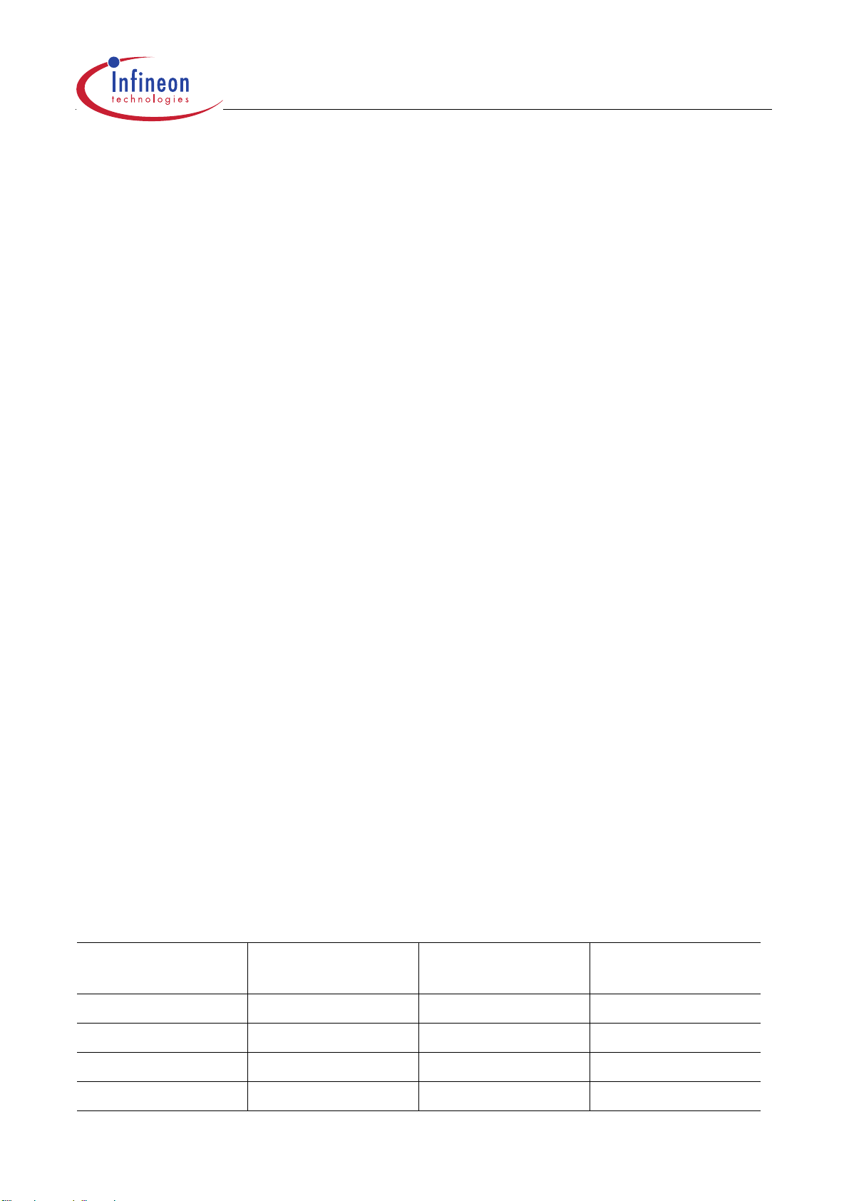
5 Functional Block Diagram
Target Datasheet TLE 6266
OUTL1
Vs
PW M
Charge
Pump
UVL O
Band
Vs
Vcc
Gap
Dr ive
Dr ive
Protection + Drive
Dr ive
Dr ive
-
+
LDO
Sw itch
Fail De tec t
SPI
Timer
Res et
Generator
+
Window
Watchdog
Mode Control
Vcc
Os c illato r
OUTL2
OUTH1
OUTH2
OUTH3
CSN
CLK
DI
DO
Vcc
RO
WK
RTL
CA NH
CA NL
RTH
H Output Stage
Filter
L Output Stage
Rec e ive r
CA N Fail Det ec t
Dr ive r
Temp.
Protect
Fail Management
Input
Stage
GND
Vcc
Tx D
Vcc
Rx D
Figure 2 TLE 6266 G Functional Block Diagram
Version 1.06 6 2002-11-26
Target Datasheet TLE 6266
6 Circuit Description
The TLE 6266 G is a monolithic IC, which incorporates a failure tolerant low speed CANtransceiver for differential mode data transmission, a low dropout voltage regulator for
internal and external 5V supply as well as a SPI interface to control and monitor the IC.
Further there are three high side switches, two low side switches, a window watchdog
circuit and a reset circuit integrated. Figure 2 shows the block diagram of the TLE 6266.
6.1 Operation Modes
The TLE 6266 offers four different operation modes (see Figure 3), that are controlled
via the SPI input bits 9,10 (mode bits M0,M1) as shown in Table 1: the normal operation
mode, the receive-only mode, the V
stand-by mode and the cyclic wake operation
bat
mode.
The cyclic wake mode itself is subdivided into two modes: the cyclic HS OFF and the
cyclic HS ON mode. Cyclic wake and V
stand-by mode are both designed for periods
bat
that do not require communication on the CAN-Bus but offer a low power mode. The
lowest current consumption is achieved in the cyclic wake mode(<70µA).
Table 1 Operation modes bit settings
Mode Bit M1
(SPI Bit 10)
Mode Bit M0
(SPI Bit 9)
Normal operation 1 1
Cyclic Wake 1 0
RxD only 0 1
stand-by 0 0
V
bat
Normal Operation Mode
The normal operation mode is designed to receive and transmit data messages as well
as to supply the ECU and control loads via HS- and LS- switches. RTL is switched to
, RTH to GND. Table 3 gives an overview about the available functions in this mode.
V
CC
RxD-only Mode
In the receive-only mode the receiver stage is activated and the transmitter stage is
deactivated. This means that data at the TxD input is not transmitted to the CAN bus but
receiving of data is still possible. The CANL line is pulled-up to VCC via the RTL output
and CANH is pulled to GND via RTH. This mode is useful in combination to a dedicated
network-management software that allows separate diagnosis for all nodes (see
Chapter 6.2). Table 3 gives an overview about the available functions in this mode.
Version 1.06 7 2002-11-26
Target Datasheet TLE 6266
V
stand-by Mode
bat
In the
V
stand-by mode the CAN transmitter and receiver stage are deactivated, to
bat
achieve a low power consumption. All other functions are active as in the normal mode
(see Table 3). The CANL line is pulled-up to battery supply voltage via the RTL output
and CANH pulled to GND via RTH. A wake-up request via a CAN message on the bus
is immediately reported to the microcontroller by setting RxD=LOW. The wake pin WK
V
is not active in this mode. A power-on condition (
V
automatically switches the TLE 6266 to
stand-by mode. Also if the supply voltage
bat
pin is supplied) or a watchdog reset,
bat
drops below the specified limits (undervoltage reset), the transceiver is automatically
V
switched to
stand-by mode or power down mode, respectively.
bat
Cyclic Wake Modes
In the cyclic wake operation mode the lowest power consumption is achieved. This mode
consists of two states, the Cyclic HS ON and the Cyclic HS OFF mode.
In the HS ON state the transmitter, receiver and all switches, except the HS3 switch, are
deactivated. The CANL line is pulled-up to battery supply voltage via the RTL output and
CANH pulled to GND via RTH. A wake-up via CAN bus message sets the RxD output to
LOW. In the HS ON state, a long open window is started. If there is no valid watchdog
trigger or a PWM transition into the HS OFF state during this time, a watchdog reset is
activated. Only a correct trigger signal on the PWM Pin causes a transition into the cyclic
HS OFF state. This is called the “failsafe PWM” feature.
In the HS OFF state, almost all functions of the IC are deactivated(also HS3-switch).
Only the wake-up input, the oscillator and the power-on reset circuit are activated. The
oscillator is used to realize the HS3-cyclic wake function.This automatically switches to
HS ON state after a programed time, to enabled HS3 (see Table 2).The CANL line is
pulled-up to battery supply voltage via the RTL output and CANH pulled to GND via RTH.
Only the wake up via CAN message sets the RxD to low (visible in HS ON state).
There are three possibilities to enter the cyclic HS ON mode from the HS OFF mode:
• the cyclic wake function
• a falling edge at the wake-up pin
• a CAN bus wake
Table 2 SPI Bit settings for the cyclic wake function
Input Bit 13 Input Bit12 Period # of Cycles
(1 cycle = 512µs typ.)
0 0 48ms 94
0 1 96ms 188
1 0 192ms 376
1 1 no cyclic wake-up -
Version 1.06 8 2002-11-26
Target Datasheet TLE 6266
SPI
SPI
Power Down
Normal Mode
M1 = 1
all functions active
SPI
RxD-Only
M1 = 0
all functions active
SPI
Cyclic Wake
Cyclic HS OFF
M1 = 1
Vcc = OFF/ON
RTL = 12V
WD = OFF
HS3 = OFF
M0 = 1
SPI
M0 = 1
M0 = 0
POR = ON
RxD = H
1)
3V SV
= ON
Start Up
Power Up
SPI
SPI
SPI
SPI
V
Stand-By
bat
M1 = 0
Vcc = ON
RTL = 12V
WD = ON
Watch
POR = ON
PWM HS1
3VSU = ON
RxD = H/L
t>T
WDR
dog
Reset
Power
ON
Reset
M0 = 0
2)
automatic transition after:
- cyclic wake time
- WK pin = H
- CAN bus wake
Cyclic HS ON
M1 = 1
Vcc = ON
RTL = 12V
WD = ON
HS3 = ON
Mode Bits:
M0 = SPI Input Bit 9
M1 = SPI Input Bit 10
Figure 3 State Diagram
3)
PWM
M0 = 0
POR = ON
RxD = H/L
1)
= ON
3V SV
1) 3V supervisor feature only active if selected via SPI
2) HS1 is controlled by the SPI input bit 1(activate HS1) and also the PWM
input pin27 if the SPI input bit 11 (PWM enable) is set. In case both
controls are active, the HS1 switch is masked by the SPI input bit 1 (see
figure 12)
3) this function makes sure that the cyclic HS OFF mode can only be
entered via a correct signal at the PWM pin
SPI
SPI
Version 1.06 9 2002-11-26
Table 3 Operation mode table
Target Datasheet TLE 6266
Feature Normal
mode
RxD only
mode
V
bat
stand-by
mode
Cyclic
Wake
HS ON
Cyclic
Wake
HS OFF
LDO ONONONONOFF/ON
Reset ONONONONON
Watchdog ON ON ON ON OFF
SPI ONONONONOFF
Oscillator ONONONONON
CAN transmit ON OFF OFF OFF OFF
CAN receive ON ON OFF OFF OFF
OUTHS 1
PWM HS1
OUTHS 2
OUTHS 3
1) 2) 3)
2)
1) 3)
1) 3)
OUTHS 3 cycl. HS
1) 3)
ON
OUTLS 1
OUTLS 2
1) 3)
1) 3)
ON ON ON OFF OFF
ON ON ON OFF OFF
ON ON ON OFF OFF
ON ON ON OFF OFF
OFF OFF OFF ON OFF
ON ON ON OFF OFF
ON ON ON OFF OFF
OUT HS 3
ON ON ON OFF OFF
Timebase-Test
Wake Pin OFF OFF OFF OFF ON
Failsafe PWM
3V Supervisor
4)
1) ON
RTL output
RxD output
1)
only active when selected via SPI
2)
HS1 is controlled by the SPI input bit 1(activate HS1) and also the PWM input pin27 if the SPI input bit 11 (PWM
enable) is set. In case both controls are active, the HS1 switch is masked by the SPI input bit 1 (see figure 12)
3)
automatically disabled when a reset resp. watchdog reset occurs
4)
this function makes sure that the cyclic HS OFF mode can only be entered via a correct signal at the PWM pin
OFF OFF OFF ON OFF
switched to
Vcc
L = bus
dominant;
H = bus
recessive
ON
switched to
Vcc
L = bus
dominant;
H = bus
recessive
ON
switched to Vsswitched to
active low on
CAN message
wake-up
ON
Vs
active low on
CAN message
wake-up
ON
switched to
Vs
active low on
CAN message
wake-up
Version 1.06 10 2002-11-26
Target Datasheet TLE 6266
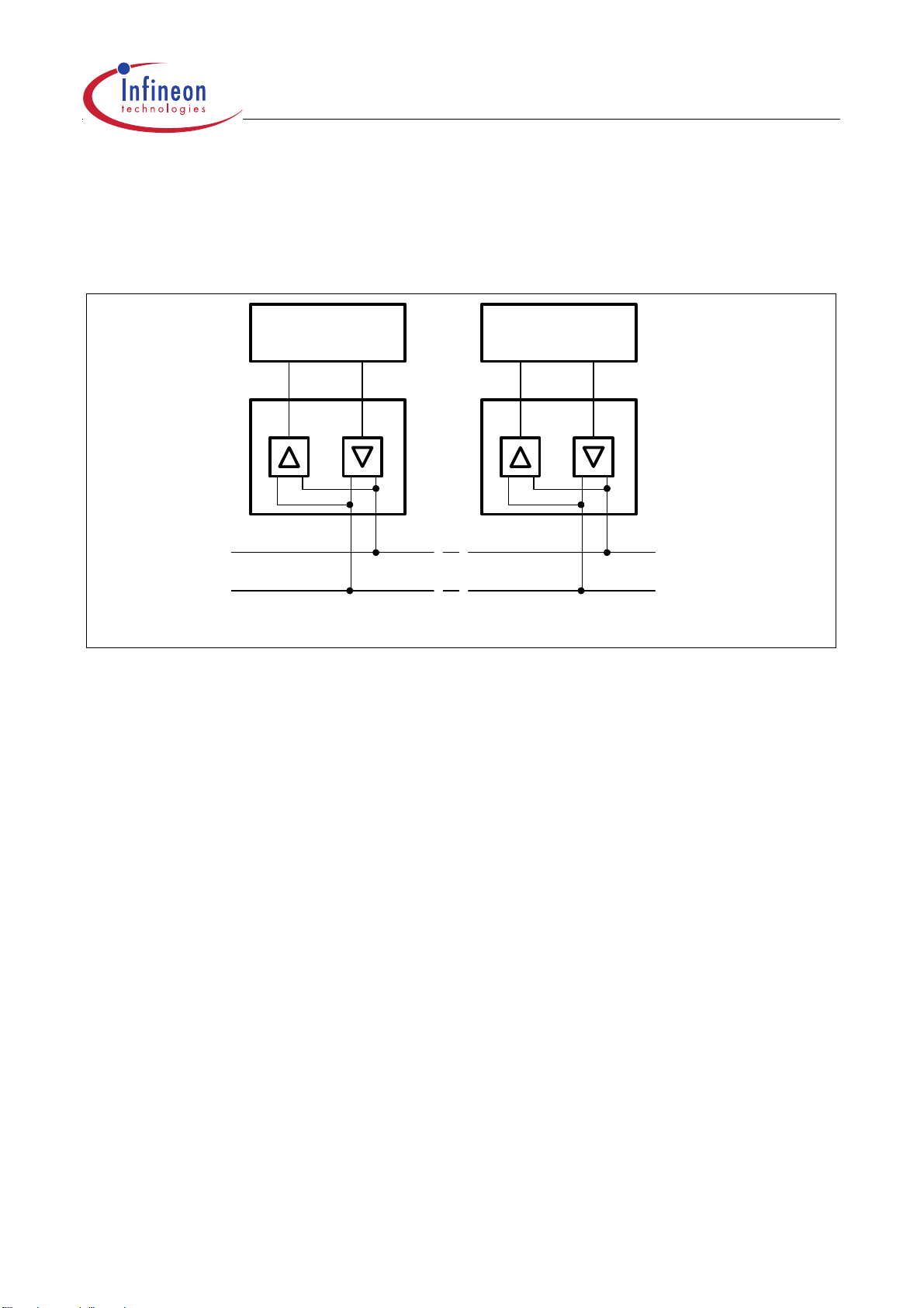
6.2 LS CAN Transceiver
The CAN transceiver TLE 6266 works as the interface between the CAN protocol
controller and the physical CAN bus-lines. Figure 4 shows the principle configuration of
a CAN network.
Controller 1
RxD1
Transceiver1
TxD1
BUS Line
Controller 2
RxD2
Transceiver2
TxD2
Figure 4 CAN Network Example
In normal operation mode a differential signal is transmitted/received. When bus wiring
failures are detected, the device automatically switches in a dedicated single-wire mode
to maintain communication. While no data is transferred, the power consumption can be
minimized by multiple low power operation modes. Further a receive-only mode is
implemented that allows a separate CAN node diagnosis. During normal and RxD-only
mode, RTL is switched to V
and RTH to GND. During V
CC
wake mode, RTL is switched to V
and RTH to GND.
S
stand-by and the cyclic
bat
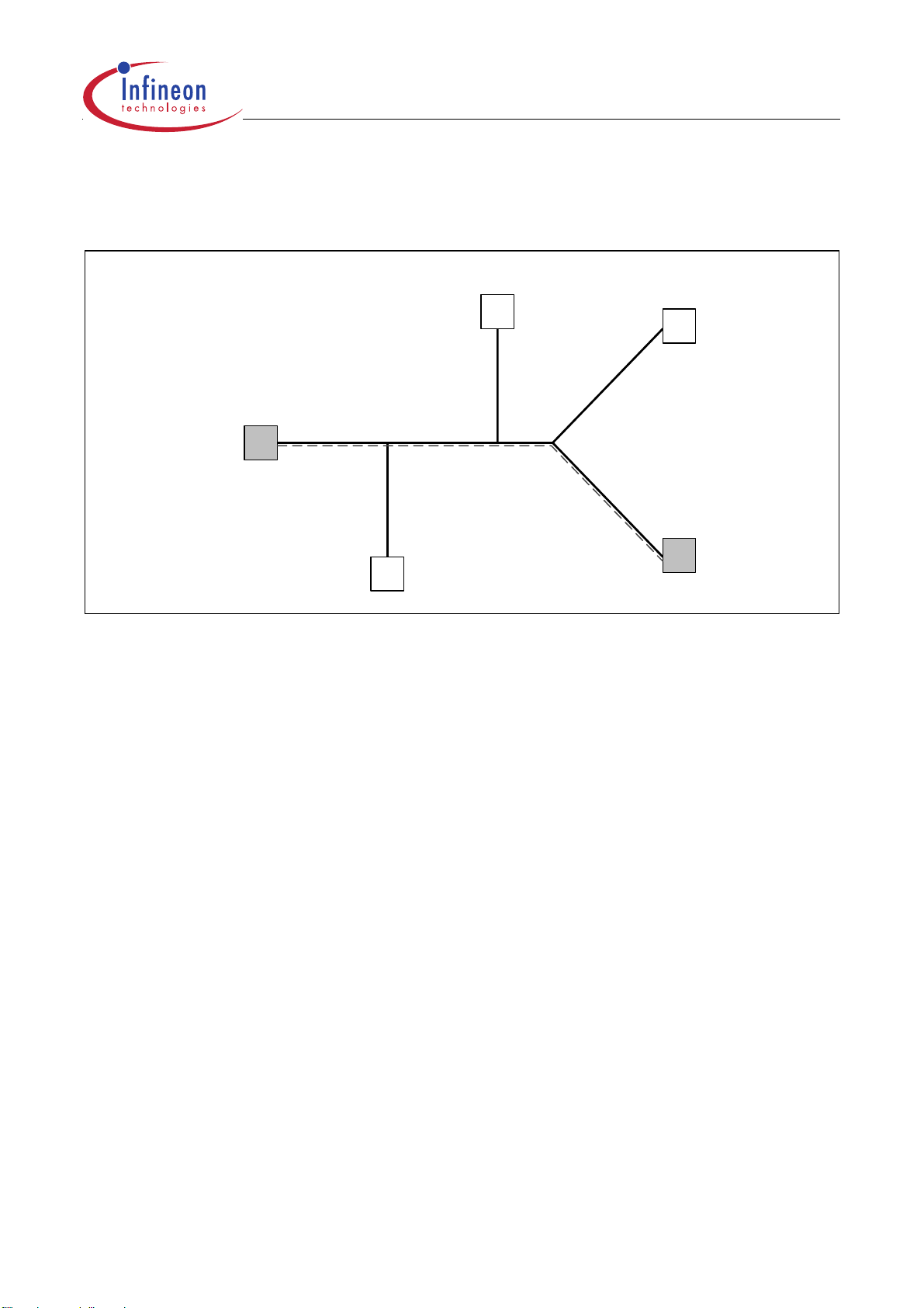
Receive-only Mode
The receive only mode is designed for a special test procedure to check the bus
connections. Figure 5 shows a network consisting of 5 nodes. If the connection between
node 1 and node 3 shall be tested, the nodes 2,4 and 5 are switched into receive only
mode. Node 1 and node 3 are in normal mode. If node 1 sends a message, node 3 is the
only node which can acknowledge the message, the other nodes can only listen but
cannot send an acknowledge bit. If node 1 receives the acknowledge bit from node 3,
the connection is OK.
Electromagnetic Emmision (EME)
To reduce radiated electromagnetic emission (EME), the dynamic slopes of the CANL
and CANH signals are both limited and symmetric. This allows the use of an unshielded
twisted or parallel pair of wires for the bus. During single-wire transmission (one of the
Version 1.06 11 2002-11-26
Target Datasheet TLE 6266
bus lines is affected by a bus line failure) the EME performance of the system is
degraded from the differential mode.
5
1
2
4
3
Figure 5 Testing the Bus Connection in Receive-only Mode
6.3 Bus Failure Management
There are 9 different CAN bus wiring failures defined by the ISO 11519-2 standard.
These failures are devided into 7 failure groups (see Table 4). When a bus wiring failure
is detected the device automatically switches to a dedicated CANH or CANL single-wire
mode to maintain the communication if necessary. Therefore it is equipped with one
differential receiver and four single ended comparators (two for each bus line).
To avoid false triggering by external RF influences, the single wire modes are activated
after a certain delay time. As soon as the bus failure disappears the transceiver switches
back to differential mode after another time delay.
The bus failures are monitored via the diagnosis protocoll of the SPI. Therefore it is
possible to distinguish 6 CAN bus failures or failure groups on the SPI output bits 8 to 13
(see Table 4 and 5). The failures are reported until transmission of the next CAN word
begins.The SPI output bit 0 for CAN bus wiring failure can be read out without SPI
transmission directly via the CSN pin (CSN=LOW). A transition of the CSN pin signal
from LOW to HIGH resets the SPI diagnosis bit 0.
The differential receiver threshold is set to typ. -2.5V. This ensures correct reception in
the normal operation mode as well as in the failure cases 1, 2, 3a and 4 with a noise
margin as high as possible. When one of the bus failures 3, 5, 6, 6a, and 7 is detected,
the defective bus wire is disabled by switching off the affected bus termination and output
stage. Simultaneously the multiplexing output of the receiver circuit is switched to the
unaffected single ended comparator.
Version 1.06 12 2002-11-26
Target Datasheet TLE 6266
Table 4 CAN bus line failure cases (according to ISO 11519-2)
Failure
Failure Description
#
1 CANL line interrupted
2 CANH line interrupted
3 CANL shorted to V
(no ISO failure) CANL shorted to V
3a
, CANL > 7.2 V
bat
; 3.2 V < CANL < 7.2 V
cc
4 CANH shorted to GND
5 CANL shorted to GND
6 CANH shorted to V
6a
(no ISO failure) CANH shorted to V
; CANH > 7.2 V
bat
; 1.8 V < CANH < 7.2 V
cc
7 CANL shorted to CANH
In case the transmission data input TxD is permanently dominant, both, the CANH and
CANL transmitting stage are disabled after a certain delay time t
. This is necessary
TxD
to prevent the bus from being blocked by a defective protocol unit or short to GND at the
TxD input.
In order to protect the transceiver output stages from being damaged by shorts on the
bus lines, current limiting circuits are integrated. The CANL and CANH output stage
respectively are protected by an additional temperature sensor, that disables them as
soon as the junction temperature exceeds the maximum value. In the temperature shutdown condition of the CAN output stages receiving messages from the bus lines is still
possible. A thermal shutdown of the CAN-transceiver circuit is monitored via the SPI
output bit 15. The CANH and CANL pins are also protected against electrical transients
which may occur in the severe conditions of automotive environments.
Table 5 SPI output bits for bus failure diagnosis
OBIT Bus Failure
13 CAN Failure 2 and 4
12 CAN Failure 1 and 3a
11 CAN Failure 6
10 CAN Failure 6a
9 CAN Failure 5 and 7
8 CAN Failure 3
0 CAN Bus Failure
Version 1.06 13 2002-11-26

Target Datasheet TLE 6266
6.4 Low Dropout Voltage Regulator
The TLE6266 is able to drive external 5V loads up to 45 mA. Its output voltage tolerance
is less than ± 2%. In addition the regulator circuit drives the internal loads like the CANtransceiver circuit. In the cyclic wake HS OFF operation mode the voltage regulator is
switched on and off by a control mechanism (see Chapter 6.5).
The current limitation of the LDO is set to typ. 180mA, to grant that the external capacitor
can be charged quickly. In normal operating mode the external current should be less
then 45mA. This has to guaranteed by the system architecture.
An external reverse current protection is recommended to prevent the output capacitor
from being discharged by negative transients or low input voltage.
Stability of the output voltage is guaranteed for output capacitors C
³ 100 nF.
VCC
Nevertheless a lot of applications require a much larger output capacitance to buffer the
output voltage in case of low input voltage or negative transients. Furthermore the due
function of e.g. the reset and 3V-supervisor circuit are supported by a larger output
capacitance because of their reaction times. Therefore a output capacitance
C
³ 22 µF is recommended.
VCC
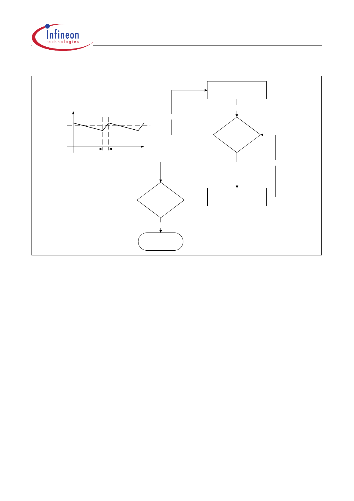
6.5 LDO activation during Cyclic Wake HS OFF
During the cyclic wake HS OFF mode, the LDO is switched on and off, depending on the
output voltage level, which is monitored internaly. Figure 6 shows a detailed flowchart
of the V
mode. The voltage regulator is switched on as soon as the voltage at V
control loop and also a graph of the Vcc voltage and the thresholds in this
cc
falls below the
CC
load-threshold to charge an external capacitor for 1ms. When the nominal voltage level
is reached again, the voltage regulator is automatically deactivated to minimize the
current consumption. The period of charging/decharging is dependant on the external
stabilization capacitor at V
CC
.
6.6 3V-Supervisor
If the output voltage falls below the 3V-supervisor threshold V
, an internal flip-flop is
ST
set LOW. The SPI output bit 7 monitors this. In normal operation this flip-flop has to be
activated via the SPI input bit 7. This feature is useful e.g. to monitor that the RAM data
of the microcontroller might be damaged or the application is connected to V
the first
S
time.
The 3V supervisor uses a comparator to monitor the voltage. Additional, there is a
possibility to disable this comparator in order to reduce the current consumption. To do
this, set SPI input bit 15 first and in the next step set SPI input bit 7.
Version 1.06 14 2002-11-26
Target Datasheet TLE 6266
Vcc
5
4
t
CHARGE
Charge Diagram
Yes
V
CC TH
V
RESET TH
t
Vcc< reset threshold
V
RESET TH
for t > 3µs ?
Yes
RESET after filtering-
time
No
Monitor V
in Cyclic wake
cc
HS OFF Mode
Vcc
Vcc > load threshold
V
CC TH
No
Charge of V
cc
(Switch on LDO)
?
Vcc
for 1ms
Figure 6 LDO activation flowchart for the cyclic wake HS OFF mode
6.7 SPI (serial peripheral interface)
The 16-bit wide programming word or input word (see Table 6) is read in via the data
input DI, and this is synchronized with the clock input CLK supplied by the µC. The
diagnosis word appears synchroniously at the data output DO (see Table 7).
The transmission cycle begins when the chip is selected by the chip select not input CSN
(H to L). After the CSN input returns from L to H, the word that has been read in becomes
the new control word. The DO output switches to tristate status at this point, thereby
releasing the DO bus for other usage.
The state of DI is shifted into the input register with every falling edge on CLK. The sate
of DO is shifted out of the output register after every rising edge on CLK. For more details
of the SPI timing please refer to Figure 11 to 15.
CAN Bus Wiring Failure direct Read-out
The SPI output bit 0 for CAN bus wiring failure can be read out without SPI transmission
directly via the CSN pin (CSN=LOW). A transition of the CSN pin signal from LOW to
HIGH resets the SPI diagnosis bit 0.
SPI CLK Monitoring during Cyclic Wake Mode
The TLE 6266 offers a feature to monitor the SPI clock signal (CLK pin) during the cyclic
wake mode. If there are edges on the CLK signal, the IC performs a reset and the RO
Version 1.06 15 2002-11-26
Target Datasheet TLE 6266
pin is set to LOW for t= t
WDR
(after t
a long open window is started and RO is HIGH
WDR
again). This feature is activated if the CSN pin is set to HIGH.
Table 6 SPI Input Data Protocol Table 7 SPI Output Data Protocol
IBIT Input Data OBIT Output Data
15 Disable 3V Reset Comparator 15 Thermal Shutdown Transceiver
14 not used 14 Thermal Shutdown Switches
13 Cyclic Wake Time Bit2 13 CAN Failure 2 and 4
12 Cyclic Wake Time Bit1 12 CAN Failure 1 and 3a
11 PWM Enable HS1 11 CAN Failure 6
10 Mode 1 10 CAN Failure 6a
9 Mode 0 9 CAN Failure 5 and 7
8 not used 8 CAN Failure 3
7 Supervisor Enable 7 3V Supervisor (Vcc < 3V)
6 LS-Switch 2 6 Status LS2
5 LS-Switch 1 5 Status LS1
4 Timebase Test 4 Temperature Prewarning for all
Switches
3 HS-Switch 3 3 Vs Undervoltage Lockout
2 HS-Switch 2 2 Window Watchdog Reset
1 HS-Switch 1 1 Overcurrent HS1
0 Watchdog Trigger 0 CAN Bus Failure
H=ON
L=OFF
H=ON
L=OFF
6.8 Oscillator
The TLE 6266 has an internal oscillator with +/-15% accuracy. The typ. frequency of the
oscillator is 125kHz. After an internal 64-times frequency divider, this gives an typ. cycle
time t
the
= 0.512ms. The frequency of the oscillator can be measured within the normal,
cyc
V
stand-by and the RxD-only mode. This is a timebase test (see Chapter 6.15),
bat
activated via SPI input bit 3 and 4. During this test, the HS3-switch will be activated
cyclically.
Version 1.06 16 2002-11-26

6.9 Window Watchdog and Reset
Target Datasheet TLE 6266
When the output voltage V
RO is switched HIGH after a delay time t
exceeds the reset threshold voltage VRT the reset output
CC
. This is necessary for a defined start of the
RD
microcontroller when the application is switched on. As soon as an under-voltage
condition of the output voltage (V
LOW again. The LOW signal is guaranteed down to an output voltage V
< VRT) appears, the reset output RO is switched
CC
³ 1V. Please
CC
refer to Figure 17, reset timing diagram.
In the cyclic wake HS OFF mode, the watchdog circuit is automatically disabled.Both,
the undervoltage reset and the watchdog reset set all SPI input bits LOW.
Long Open Window
After the delayed reset (LOW to HIGH transition of RO) the window watchdog circuit is
started by opening a long open window. The long open window allows the
microcontroller to run his set-up and to trigger the watchdog via the SPI afterwards.
Within the long open window period a watchdog trigger is alternating detected as a
“rising” or “falling edge” by sampling a HIGH on the SPI input bit 0. The trigger is
accepted when the CSN input becomes HIGH after the transmission of the SPI word.
After every reset condition (watchdog reset, undervoltage reset) as well as a transition
in the cyclic wake mode from HS OFF to HS ON, the watchdog starts the long open
window and the default value of the SPI input bit 0 is LOW.
Closed/Open Window
A correct watchdog trigger immediately results in starting the window watchdog by
opening the closed window followed by the open window (see Figure 18). From now on
the microcontroller has to service the watchdog trigger by inverting the SPI input bit 0
alternating. The “negative” or “positive” edge has to meet the open window time. A
correct watchdog service immediately results in starting the next closed window. Please
refer to Figure 19, watchdog timing diagram.
Watchdog Trigger Failure
If the trigger signal does not meet the open window a watchdog reset is created by
setting the reset output RO low for t
. Then the watchdog starts again by opening the
WDR
long open window. In addition, the SPI output bit 2 is set HIGH until the next successful
watchdog trigger, to monitor a watchdog reset. SPI output bit 2 is also HIGH until the
watchdog is correctly triggered after power-up/start-up. For fail safe reasons the
TLE6266 is automatically switched in V
stand-by mode if a watchdog trigger failure
bat
occurs.
6.10 High Side Switch 1
The high side output OUTH1 is able to switch loads up to 250 mA. Its on-resistance is
1.0 W typ. @ 25°C. This switch can be controlled either via the PWM input or the SPI
input bit 1. When the input PWM is used, it has to be enabled by setting the SPI input bit
Version 1.06 17 2002-11-26

Target Datasheet TLE 6266
11 HIGH. In case of both control inputs being active the PWM signal is masked by the
SPI signal (see Figure 16, High Side Switch 1 Timing Diagram).
The SPI output bit 14 monitors a thermal shutdown of the switches, whereas output bit
4 flags a thermal prewarning. So the microcontroller is able to reduce the power
dissipation of the TLE 6266 by switching off functions of minor priority before the
temperature threshold of the thermal shutdown is reached. Further OUTH1 is protected
against short circuit and overload. The SPI output bit 1 indicates an overload of OUTH1.
As soon as the under-voltage condition of the supply voltage is met (V
< V
S
UVOFF
), the
switches are automatically disabled by the under-voltage lockout circuit. This is flagged
by the SPI output bit 3. Moreover the switch is disabled when a reset occurs. After the
second correct triggered watchdog, the switch is released for usage.
6.11 High Side Switch 2
The high side output OUTH2 is able to switch loads up to 250 mA. Its on-resistance is
1.0 W typ. @ 25°C. This switch is controlled via the SPI input bit 2.
The SPI output bit 14 monitors a thermal shutdown of the switches, whereas output bit
4 flags a thermal prewarning. So the microcontroller is able to reduce the power
dissipation of the TLE 6266 by switching off functions of minor priority before the
temperature threshold of the thermal shutdown is reached. As soon as the under-voltage
condition of the supply voltage is met (V
< V
S
UVOFF
), the switches are automatically
disabled by the under-voltage lockout circuit. This is flagged by the SPI output bit 3.
Moreover the switch is disabled when a reset occurs. After the second correct triggered
watchdog, the switch is released for usage.
6.12 High Side Switch 3
The high side output OUTH3 is able to switch loads up to 250 mA. Its ON-resistance is
1.0 W typ. @ 25°C. This switch is controlled via the SPI input bits 3 and 4. To supply
external wake-up circuits in low power mode (cyclic wake mode), the output OUTH3 is
periodically activated by entering the cyclic wake HS ON mode. The autotiming period
is programable via SPI (see Table 2).This has to be done, to minimize the current
consumption depending on the cyclic wake time (see Figure 21).
In the cyclic wake mode, the PWM signal is used to switches HS3 from the cyclic HS ON
to the cyclic HS OFF state, if correctly triggered within the long open window (see Figure
17). This is called the “fail-safe PWM” feature
The SPI output bit 14 monitors a thermal shutdown of the switches, whereas output bit
4 flags a thermal prewarning. So the microcontroller is able to reduce the power
dissipation of the TLE 6266 by switching off functions of minor priority before the
temperature threshold of the thermal shutdown is reached. As soon as the under-voltage
condition of the supply voltage is met (V
< V
S
UVOFF
), the switches are automatically
disabled by the under-voltage lockout circuit. This is flagged by the SPI output bit 3.
Version 1.06 18 2002-11-26

Target Datasheet TLE 6266
Moreover the switch is disabled when a reset occurs. After the second correct triggered
watchdog, the switch is released for usage.
6.13 Low Side Switches 1 & 2
The two low side outputs OUTL1 and OUTL2 are able to switch loads up to 100 mA.
Their on-resistance is 1.5 W typ. @ 25°C. This switches are controlled via the SPI input
bits 5 and 6. In case of high inrush currents a built in zener circuit (typ. 37 V) activates
the switches to protect them.
The SPI diagnosis bit 14 monitors a thermal shutdown of the switches, whereas bit 4
flags a thermal prewarning. So the microcontroller is able to reduce the power dissipation
of the TLE 6266 by switching off functions of minor priority before the temperature
threshold of the thermal shutdown is reached. The SPI output bits 5/6 are giving a
feedback about current status (ON/OFF) of OUTL1/OUTL2. As soon as the undervoltage condition of the supply voltage is met (V
< V
S
UVOFF
), the switches are
automatically disabled by the under-voltage lockout circuit. This is flagged by the SPI
diagnosis bit 3. In addition the outputs OUTL1 and OUTL2 are disabled when a reset
occurs. After the second correct triggered watchdog, the switches are released for
usage.
6.14 Wake Up Pin
This pin is used to wake up the TLE 6266 with an external signal from the µC. The
feature is active during cyclic HS OFF mode to switch the transceiver into the cyclic HS
ON mode before starting up the µC. A correct wake up signal is a rising edge at the WK
pin during cyclic HS OFF mode. The WK pin has an implemented pull down resistance.
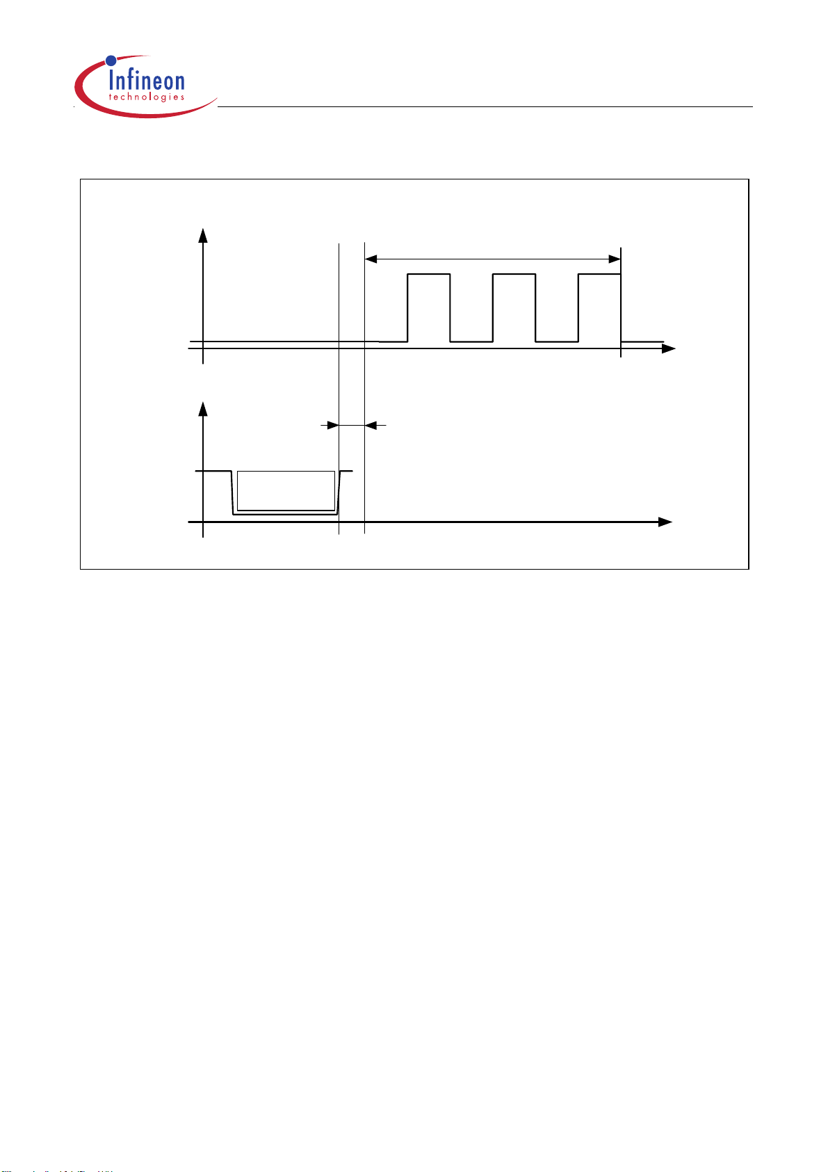
6.15 Timebase Test
This test is useful to measure the internal cycle time of the TLE 6266. The µC may use
this information to activate special functions or routines in the cyclic wake mode, which
are depending on timing.(e.g. to switch on/off a LED after a certain number of cyclic HS
ON conditions). During the long open window the timebase test is not available.
To measure the internal cyclic timing, the SPI input bit 3 and 4 have to be set HIGH. Then
the HS3 switch is automatically enabled for 3 times during the closed window of the
watchdog (see Figure 7). A correct SPI input word (with IBit 3 and 4 set HIGH) has to
be read in first, to activate the timebase test. Due to he fact, that the input command gets
activated after the CSN LOW to HIGH transition, it takes t=t
test. If this SPI input command is given within the open window, t
to activate the timebase
SYNC
=max 500ns. If the
SYNC
command is given during closed window (this is not a watchdog trigger command) the
synchronisation t
SYNC
can last up to 500µs.
Version 1.06 19 2002-11-26
HS3
ON
Target Datasheet TLE 6266
closed window (12 cycles)
2cycl.
2cycl. 2cycl.
OFF
2cycl.
2cycl. 2cycl.
t
CSN
SPI Input word with
timebase test
command
t
SYNC
t
Figure 7 Timebase Test Diagram
6.16 Flash program mode
To disable the watchdog feature a flash program mode is available. This mode is
selected by applying a voltage of 6.8V < V
< 7.2V at pin PWM. This is useful e.g. if
PWM
the flash-memory of the micro has to be programmed and therefore a regular watchdog
triggering is not possible. If the SPI is required in the flash program mode to change e.g.
the mode of the TLE6266, the first input telegram has to be “00000000”.
Version 1.06 20 2002-11-26

Target Datasheet TLE 6266
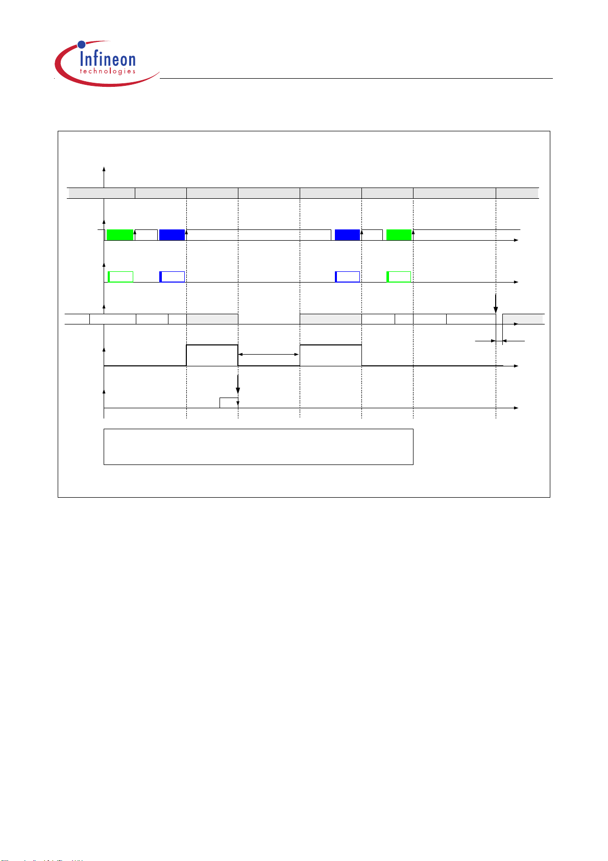
7 Explanation of the Mode Transitions
To better understand the description, the reader has to be familiar with the Chapter 6.
All descriptions are starting from the normal mode, as the main operation mode. This
means, the component was powered up before and after the power up procedure
automaticaly in the V
stand-by mode.
bat
Now, the watchdog circuit has to be operated correctly to switch the component in the
other modes ( details see Chapter 6). So the starting point is the TLE 6266 in normal
mode with a correct triggered watchdog like shown in Figure 8,9,10.
Normal Mode and Cyclic HS ON
In normal mode, the watchdog has to be triggered within the open window with a
dedicated SPI input command (Watchdog Trigger IBit 0, alternatively HIGH, LOW,...).
The CAN bus communication is active and a message can be transfered/received. After
the correct SPI input command to change into the Cyclic HS mode, the HS3 switch gets
activated. In parallel a long open window is started, wich has to be triggered. This mode
can be operated as long as the watchdog is triggered correctly. In this mode, no
communication is possible but an external circuit can be supplied by HS3. CANL is
pulled up to Vs by the RTL termination, CANH is pulled to GND via RTH.
Cyclic HS OFF mode
To switch from HS ON to HS OFF, the PWM input has to be triggered with a falling egde.
This is called the PWM failsafe trigger to avoid unwanted transitions into the HS OFF
mode. In the HS OFF mode the HS3 switch is deactivated and the lowest power
consumption is achieved. The LDO monitors Vcc and switches on/off due to a special
control mechanism explained in Chapter 6.5. Three possibilities can switch the TLE
6266 back to the cyclic wake HS ON mode:
7.1 CAN Bus Wake-Up
CANL is pulled to Vs. A signal transition at CANL below a certain wake-up threshold
causes a wake up and automatic transition into the cyclic HS ON mode (see Figure 8).
HS3 is activated again and also the long open window of the watchdog mechanism. The
watchdog has to be triggered correctly from that time on. If the signal at the PWM pin
makes a HIGH to LOW transition, the device switches to HS OFF again.
This wake up via the CAN bus message is flagged to the µC by setting the RxD output
pin from HIGH to LOW. The reason for this behavior is to indicate the µC a wake up
request. Now, the µC is able to activate the whole module to serve the requested action
by the bus system.
Version 1.06 21 2002-11-26

Target Datasheet TLE 6266
Mode State
closed
window
Normal Mode
CSN,
SPI word*
Watchdog trigger bit
=SPI bit0**
Normal Mode Cyclic HS ON Cyclic HS OFF
SPI
normal
mode
Window watchdog***
open
window
closed
window
HS3
PWM
Vs
CANL
Vcc
CANH
* for the exact timing relations between CSN
and SPI-DI and -DO word please look at
datasheet fig. 11,12,13,14,15
SPI
cyclic HS
ON
open
window
long open window
PWM trig ger
PWM
trigger
** bit0 is transfered with the SPI input word
BUT
the watchdog trigger is set, after readout of
the SPI input bit = CSN LOW to HIGH
(see arrows at CSN signal)
CAN Bus message
Input filtering time t
Cyclic HS ON
SPI
cyclic HS
ON
long open window
Bus
Wake
trigger
IFT
*** for a correct watchdog triggering:
closed window must always exceed 12 cycles
open window is max. 20 cycles
long open window is max. 128 cycles
otherwise
a watchdog reset will be generated
Cyclic HS ON
normal
mode
closed
window
SPI
open
window
Normal Mode Vbat Stdby
missing trigger =
timeout =
closed
window
Watchdog Reset
open
window
Watchdog reset pulse time t
WDR
t
t
long open window
t
t
t
t
Figure 8 Cyclic Wake with CAN Message Wake-up
7.2 Wake-Up via Wake Pin
CANL is pulled to Vs. A signal transition at the wake pin WK from LOW to HIGH (rising
edge) causes a wake up and automatic transition into the cyclic HS ON mode (see
Figure 9). HS3 is activated again and also the long open window of the watchdog
mechanism. The watchdog has to be triggered correctly from that time on. If the signal
at the PWM pin makes a HIGH to LOW transition, the device switches to HS OFF again.
This wake up via the wake pin is comming from an external circuitry (switch, etc.) and
is not flagged by the RxD.
Version 1.06 22 2002-11-26

Mode State
Target Datasheet TLE 6266
closed
window
Normal Mode
CSN,
SPI word*
Watchdog trigger bit
=SPI bit0**
Window watchdog***
open
window
HS3
PWM
Wake
* for the exact timing relations between CSN
and SPI-DI and -DO word please look at
datasheet fig. 11,12,13,14,15
Normal Mode Cyclic HS ON Cyclic HS OFF
SPI
normal
mode
closed
window
SPI
cyclic HS
ON
open
window
long open window
PWM trigge r
PWM
trigger
** bit0 is transfered with the SPI input word
BUT
the watchdog trigger is set, after readout of
the SPI input bit = CSN LOW to HIGH
(see arrows at CSN signal)
wake trigger
Wake event
Input filtering time t
Cyclic HS ON
SPI
cyclic HS
ON
long open window
IFT
*** for a correct watchdog triggering:
closed window must always exceed 12 cycles
open window is max. 20 cycles
long open window is max. 128 cycles
otherwise
a watchdog reset will be generated
Cyclic HS ON
normal
mode
closed
window
SPI
open
window
Normal Mode Vbat Stdby
missi ng trigg er =
timeout =
Watchdog Reset
closed
window
Watchdog reset pulse time t
open
window
WDR
t
t
long open window
t
t
t
t
Figure 9 Cyclic Wake with Wake Pin
7.3 Wake-Up Cyclic Wake Autotiming Function
CANL is pulled to Vs. After the transition from HS ON to HS OFF, an autotiming function
is started. This is a timer controled by the internal oscillator, which can be programed by
SPI IBit 12,13. If the timer exceeds the programed time this causes a wake up and
automatic transition into the cyclic HS ON mode (see Figure 10). HS3 is activated again
and also the long open window of the watchdog mechanism. The watchdog has to be
triggered correctly from that time on. If the signal at the PWM pin makes a HIGH to LOW
transition, the device switches to HS OFF again.
This wake up via the autotiming function is not flagged to the µC by setting the RxD pin.
Version 1.06 23 2002-11-26
Mode State
Target Datasheet TLE 6266
closed
window
Normal Mode
CSN,
SPI word*
normal
Watchdog trigger bit
=SPI bit0**
Normal Mode Cyclic HS ON
SPI
mode
Window watchdog** *
open
window
closed
window
HS3
PWM
* for the exact timing relations between CSN
and SPI-DI and -DO word please look at
datasheet fig. 11,12,13,14,15
SPI
cyclic HS
ON
open
window
Cyclic HS OFF
long open window
Cyclic wake time
48ms selected
PWM trigger
PWM
trigger
** bit0 is transfered with the SPI input word
BUT
the watchdog trigger is set, after readout of
the SPI input bit = CSN LOW to HIGH
(see arrows at CSN signal)
48ms
Cyclic HS ON
long open window
*** for a correct watchdog triggering:
closed window must always exceed 12 cycles
open window is max. 20 cycles
long open window is max. 128 cycles
otherwise
a watchdog reset will be generated
SPI
cyclic HS
ON
Cyclic HS ON
SPI
normal
mode
closed
window
open
window
Normal Mode Vbat Stdby
missing trigger =
timeout =
Watchdog Reset
closed
window
Watchdog reset pulse time t
open
window
WDR
t
t
long open window
t
t
t
Figure 10 Cyclic Wake with Cyclic Wake Autotiming Function
Version 1.06 24 2002-11-26

Target Datasheet TLE 6266
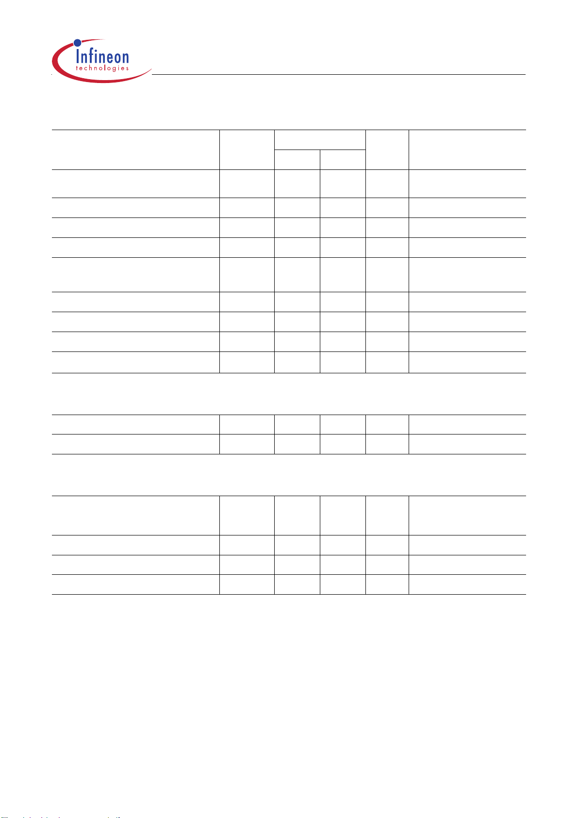
8 Electrical Characteristics
8.1 Absolute Maximum Ratings
Parameter Symbol Limit Values Unit Remarks
min. max.
Voltages
Supply voltage
Supply voltage
V
V
Regulator output voltage V
CAN input voltage
CAN input voltage
(CANH, CANL) V
V
(CANH, CANL)
Transient voltage at CANH
and CANL
Logic input voltages ( DI, CLK,
CSN, WK, PWM, TxD)
Logic output voltage
(DO, RO, RxD)
Termination input voltage
(RTH, RTL)
Electrostatic discharge
voltage at pin CANH, CANL
V
V
V
V
V
S
S
CC
CANH/L
CANH/L
BUS
I
DO/RO/RD
TL /TH
ESD
-0.3 28 V
-0.3 40 V
-0.3 5.5 V
-10 28 V
-40 40 V
– 150 100 V
-0.3 V
CC
V
+0.3
-0.3 V
CC
V
+0.3
-0.3 V
S
V
+0.3
-4000 4000 V
tp< 0.5s; tp/T < 0.1
VS >0 V
t
< 0.5s; tp/T < 0.1
p
see ISO 7637
human body model;
C = 100pF, R = 1.5kW
Electrostatic discharge
voltage to any other pin
V
ESD
-2000 2000 V
human body model;
C = 100pF, R = 1.5kW
Currents
Output current; Vcc
Output current; OUTH1 I
Output current; OUTH2 I
Output current; OUTH3 I
Output current; OUTL1 I
Output current; OUTL2 I
I
CC
OUTH1
OUTH2
OUTH3
OUTL1
OUTL2
*0,2A
*0.3A
-0.7 0.3 A
-0.7 0.3 A
-0.2 0.4 A
-0.2 0.4 A
Version 1.06 25 2002-11-26
* internally limited
* internally limited
tp< 0.5s; tp/T < 0.1
tp< 0.5s; tp/T < 0.1
tp< 0.5s; tp/T < 0.1
tp< 0.5s; tp/T < 0.1

Target Datasheet TLE 6266
8.1 Absolute Maximum Ratings (cont’d)
Parameter Symbol Limit Values Unit Remarks
min. max.
Temperatures
Junction temperature
Storage temperature
Note: Maximum ratings are absolute ratings; exceeding any one of these values may cause
irreversible damage to the integrated circuit.
T
j
T
stg
-40 150 °C
-50 150 °C
Version 1.06 26 2002-11-26
Target Datasheet TLE 6266
8.2 Operating Range
Parameter Symbol Limit Values Unit Remarks
min. max.
Supply voltage
V
Supply voltage slew rate dV
Supply voltage increasing
V
Supply voltage decreasing V
Logic input voltage (DI, CLK,
V
CSN, PWM, TxD )
Output current
Output capacitor
SPI clock frequency
Junction temperature
I
C
f
T
CC
CLK
j
Thermal Resistances
Junction pin
R
Junction ambient R
S
/dt -0.5 5 V/ms
S
S
S
I
V
UV OFF
-0.3 V
-0.3 V
-0.3 V
27 V
UV ON
UV OFF
CC
45 mA
CC
22 mF
–1MHz
-40 150 °C
thj-pin
thj-a
–25K/W
–65K/W
V
V
V
After VS rising above
V
Outputs in tristate
Outputs in tristate
measured to pin 7
UV ON
Thermal Prewarning and Shutdown (junction temperatures)
Thermal prewarning
T
jPW
120 170 °C
ON temperature
Thermal shutdown temp. T
Ratio of SD to PW temp. T
Thermal shutdown temp. CAN
jSD
/ T
jSD
T
jSD
150 200 °C
1.05 – –
jPW
135 160 °C
bit 0 of SPI diagnosis
word;
hysteresis 30°K (typ.)
hysteresis 30°K (typ.)
hysteresis 10°K (typ.)
Version 1.06 27 2002-11-26
Target Datasheet TLE 6266
8.3 Electrical Characteristics
9V<VS< 16 V; ICC= -100 mA; normal mode; all outputs open; – 40 °C<Tj<150°C; CAN-
T
transceiver circuitry: – 40 °C<
< 125 °C; all voltages with respect to ground; positive current
j
defined flowing into pin; unless otherwise specified.
Parameter Symbol Limit Values Unit Test Condition
min. typ. max.
Quiescent current Pin
Current consumption I
Quiescent current
I
= IS - I
SSB1
CC
Static quiescent current I
Voltage Regulator; Pin
Output voltage V
Output voltage V
Line regulation ,V
Load regulation ,V
V
V
S
–810mA
–75100mA
––70mA
4.95.05.1V
4.85.05.5V
-20 20 mV
-25 25 mV
CC
S
I
SSB1
STAT
CC
CC
CC
CC
Power supply ripple rejection PSRR 40 dB
Output current limit I
Dropvoltage
VDR = VS - V
CC
CCmax
V
DR
155 - - mA
0.15 0.45 V
normal mode
cycl. wake 48ms;
V
=12V; Tj=25°C
S
0.1mA < ICC< 30mA
0A < I
9V<VS< 15 V;
I
CC
0.1mA < ICC< 30mA;
V
S
VS< 1 Vss;
C
Q
100Hz< f <100kHz
1)
I
CC
see note 1)
CC
= 10mA
=9V
³ 22µF;
= 30 mA;
< 100µA
Wake-up Input WK
Input current
H-input voltage threshold
L-input voltage threshold
Hysteresis of input voltage
Input filtering time
1) measured when output voltage VCC dropped 100 mV from the nom. value obtained at 13.5 V inp. voltage V
I
V
V
V
t
IL
IH
IL
IHY
IFT
Version 1.06 28 2002-11-26
–3 –2 –1 mA
––0.7 ´
V
CC
0.2 ´
V
CC
––V
V
50 200 500 mV
––3µs
S

Target Datasheet TLE 6266
8.3 Electrical Characteristics (cont’d)
9V<VS< 16 V; ICC= -100 mA; normal mode; all outputs open; – 40 °C<Tj< 150 °C; CAN-
T
transceiver circuitry: – 40 °C<
<125°C; all voltages with respect to ground; positive current
j
defined flowing into pin; unless otherwise specified.
Parameter Symbol Limit Values Unit Test Condition
min. typ. max.
Oscillator
Oscillator frequency f
Cycle time
f
osc
t
(guaranteed by design)
Reset Generator; Pin RO
Reset threshold voltage
Reset low output voltage
V
V
Reset high output voltage V
Reset pull up current
I
Reset reaction time t
Reset reaction time t
OSC
CYC
RT
RO
RO
RO
RR
RR
125 kHz
512 µs
+/-15% accuracy
64 times frequency
divider
4.0 4.3 4.65 V
0.2 0.4 V
4.0 VCC+
V
I
(V
V
(I
0.1
20 150 500 mA
1310µs
––50µs
V
V
RO = L; normal, RxD,
stand-by mode
V
RO = L; cyclic wake
mode
RO
CC
CC
RO
RO
CC
CC
= 1mA
³ VRT) or
³ 1V
= 200 µA)
= 0V
< V
to
RT
< V
to
RT
Reset delay time (16 cyl.) t
RD
6.1 8.1 10.2 ms
3 V Supervisor; (bit 7 of SPI output word)
Supervisor threshold voltage
Supervisor reaction time
V
t
ST
SR
2.32.73.1V
2820µs
V
diagnosis bit 7 = L
CC
< V
ST
to
Watchdog Generator
Watchdog trigger time
Closed window time (12 cyl.)
t
t
WD
CW
Version 1.06 29 2002-11-26
7.6 10 12.3 ms
4.66.17.6ms

Target Datasheet TLE 6266
8.3 Electrical Characteristics (cont’d)
9V<VS< 16 V; ICC= -100 mA; normal mode; all outputs open; – 40 °C<Tj<150°C; CAN-
T
transceiver circuitry: – 40 °C<
< 125 °C; all voltages with respect to ground; positive current
j
defined flowing into pin; unless otherwise specified.
Parameter Symbol Limit Values Unit Test Condition
min. typ. max.
Open window time (20 cyl.) t
Watchdog reset-pulse time
OW
t
WDR
7.7 10.2 12.7 ms
1.52.02.6ms
(4 cyl.)
Long open window (128 cyl.)
t
LOW
65 ms
Under-Voltage Lockout (bit 3 of SPI output word)
UV-Switch-ON voltage
V
UV-Switch-OFF voltage V
UV-ON/OFF-Hysteresis V
UV ON
UV OFF
UV HY
– 5.35 6.00 V
4.50 4.85 5.20 V
–0.5–V
PWM Input to control OUTH1; Pin PWM (high active)
H-input voltage threshold
L-input voltage threshold
V
V
IH
IL
––0.7 ´
0.2 ´
V
cc
––V
V
CC
V
VS increasing
VS decreasing
V
UV ON
– V
UV OFF
Hysteresis of input voltage
Pull down current
Input capacitance C
V
I
I
IHY
I
50 200 500 mV
525180mA
–1015pF
VI = 0.2 * V
0V < V
< 5.25 V
CC
CC
Version 1.06 30 2002-11-26
Target Datasheet TLE 6266
8.3 Electrical Characteristics (cont’d)
9V<VS< 16 V; ICC= -100 mA; normal mode; all outputs open; – 40 °C<Tj< 150 °C; CAN-
T
transceiver circuitry: – 40 °C<
<125°C; all voltages with respect to ground; positive current
j
defined flowing into pin; unless otherwise specified.
Parameter Symbol Limit Values Unit Test Condition
min. typ. max.
Switches
High Side Output OUTH1; (controlled by PWM or bit 1 of SPI input word)
Static Drain-Source
R
ON-Resistance;
I
OUTH1
= -0.25 A
Active zener voltage V
Clamp diode forward voltage V
Leakage current I
Switch ON delay time t
Switch OFF delay time t
Overcurrent shutdown
I
DSON H1
OUTH1
OUTH1
OLH1
dONH1
dOFFH1
SDH1
–1.02.0W
1.5 4.0 W
-5.0 -3.0 -0.5 V
0.8 1 V
-100 -5 – µA
10 100 ms
20 100 ms
-1.0 -0.6 -0.3 A
threshold
Shutdown delay time
Current limit
t
dSDH1
I
OCLH1
10 25 50 ms
-2.0 -1.0 -0.5 A
High Side Output OUTH2; (controlled by bit 2 of SPI input word)
5.2 V £ VS £ 9V
I
= – 0.25 A
OUTH1
I
= 0.25 A
OUTH1
V
PWM to OUTH1;
R
PWM to OUTH1;
R
OUTH1
= 100 W
L
= 100 W
L
= 0 V
Static Drain-Source
R
ON-Resistance;
I
OUTH2
= -0.25 A
Active zener voltage V
Clamp diode forward voltage V
Leakage current I
Switch ON delay time t
Switch OFF delay time t
DSON H2
OUTH2
OUTH2
OLH1
dONH1
dOFFH1
–1.02.0W
1.5 4.0 W
-5.0 -3.0 -0.5 V
0.8 1 V
-100 -5 – µA
10 100 µs
20 100 µs
5.2 V £ VS £ 9V
I
= – 0.25 A
OUTH2
I
= 0.25 A
OUTH2
V
CSN high to OUTH2;
R
CSN high to OUTH2;
R
OUTH2
= 100 W
L
= 100 W
L
= 0 V
Version 1.06 31 2002-11-26
Target Datasheet TLE 6266
8.3 Electrical Characteristics (cont’d)
9V<VS< 16 V; ICC= -100 mA; normal mode; all outputs open; – 40 °C<Tj<150°C; CAN-
T
transceiver circuitry: – 40 °C<
< 125 °C; all voltages with respect to ground; positive current
j
defined flowing into pin; unless otherwise specified.
Parameter Symbol Limit Values Unit Test Condition
min. typ. max.
High Side Output OUTH3; (controlled by bit 3 and bit 4 of SPI input word)
Static Drain-Source
R
ON-Resistance;
I
OUTH3
= -0.25 A
Active zener voltage V
Clamp diode forward voltage V
Leakage current I
Switch ON delay time t
Switch OFF delay time t
DSON H3
OUTH3
OUTH3
OLH3
dONH3
dOFFH3
–1.02.0W
1.5 4.0 W
-5.0 -3.0 -0.5 V
0.8 1 V
-100 -5 – µA
10 100 µs
20 100 µs
Low Side Output OUTL1 ( bit 5 of SPI input word)
Static Drain-Source
R
ON-Resistance;
I
OUTL1
= 0.1 A
Active zener clamp voltage V
Leakage current I
Switch ON delay time t
Switch OFF delay time t
DSON L1
OUTL1
OLL1
dONL1
dOFFL1
–1.53.0W
2.0 5.0 W
32 37 42 V
550µs
550µs
5.2 V £ VS £ 9V
I
OUTH3
I
OUTH3
V
CSN high to OUTH3;
R
CSN high to OUTH3;
R
5.2 V £ VS £ 9V
I
OUTL1
5µA
V
T
CSN high to OUTL1;
R
CSN high to OUTL1;
R
OUTH3
= 100 W
L
= 100 W
L
= + 0.1 A
OUTL1
< 85°C
j
= 100 W
L
= 100 W
L
= – 0.25 A
= 0.25 A
= 0 V
=15 V;
Low Side Output OUTL2 ( bit 6 of SPI input word)
Static Drain-Source
R
DSON L2
ON-Resistance;
I
Version 1.06 32 2002-11-26
OUTL2
= 0.1 A
–1.53.0W
2.0 5.0 W
5.2 V £ VS £ 9V

Target Datasheet TLE 6266
8.3 Electrical Characteristics (cont’d)
9V<VS< 16 V; ICC= -100 mA; normal mode; all outputs open; – 40 °C<Tj< 150 °C; CAN-
T
transceiver circuitry: – 40 °C<
<125°C; all voltages with respect to ground; positive current
j
defined flowing into pin; unless otherwise specified.
Parameter Symbol Limit Values Unit Test Condition
min. typ. max.
I
Active zener clamp voltage V
Leakage current I
Switch ON delay time t
Switch OFF delay time t
OUTL2
OLL2
dONL2
dOFFL2
32 37 42 V
5µA
550µs
550µs
= + 0.1 A
OUTL2
V
T
CSN high to OUTL2;
R
CSN high to OUTL2;
R
OUTL2
< 85°C
j
= 100 W
L
= 100 W
L
=15 V;
Timebase Test TBT(bit 4 of SPI input word)
HS3 ON timing
HS3 OFF timing
# of HS activations for TBT
t
TBON
t
TBOFF
n
TBT
2 cycl.
2 cycl.
2
Version 1.06 33 2002-11-26

Target Datasheet TLE 6266
8.3 Electrical Characteristics (cont’d)
9V<VS< 16 V; ICC= -100 mA; normal mode; all outputs open; – 40 °C<Tj<150°C; CAN-
T
transceiver circuitry: – 40 °C<
defined flowing into pin; unless otherwise specified.
< 125 °C; all voltages with respect to ground; positive current
j
Parameter Symbol Limit Values Unit Test Condition
min. typ. max.
CAN-Transceiver
Receiver Output R´D
HIGH level output voltage
V
LOW level output voltage V
Transmission Input T´D
HIGH level input voltage
V
threshold
LOW level input voltage
V
threshold
HIGH level input current
I
LOW level input current I
Bus Lines CANL, CANH
Differential receiver
V
recessive-to-dominant
threshold voltage
OH
OL
IH
IL
IH
IL
dRxD(rd)
V
CC
–
V
CC
V
– 0.9
0–0.9V
0.7 ´
V
CC
– V
+ 0.3
CC
-0.3 – 0.3 ´
V
CC
V
V
-200 -50 -10 µA
-800 -200 -40 µA
–2.8 –2.5 –2.2 V
I0 = – 250µA
I
= 1.25mA
0
Vi = 4 V
Vi = 1 V
VCC=5.0V
Differential receiver
V
dRxD(dr)
–3.2 –2.9 –2.6 V
VCC=5.0V
dominant-to-recessive
threshold voltage
CANH recessive output
V
CANH,r
0.10 0.15 0.30 V
voltage
CANL recessive output
voltage
CANH dominant output
voltage
Version 1.06 34 2002-11-26
V
CANL,r
V
CANH,dVCC
V
CC
– 0.2
– 1.4
––V
V
CC
– 1.0
V
CC
V
TxD = VCC;
R
< 4 kW
RTH
TxD = VCC;
R
< 4 kW
RTL
TxD = 0 V;
I
= – 40 mA
CANH

Target Datasheet TLE 6266
8.3 Electrical Characteristics (cont’d)
9V<VS< 16 V; ICC= -100 mA; normal mode; all outputs open; – 40 °C<Tj< 150 °C; CAN-
T
transceiver circuitry: – 40 °C<
<125°C; all voltages with respect to ground; positive current
j
defined flowing into pin; unless otherwise specified.
Parameter Symbol Limit Values Unit Test Condition
min. typ. max.
CANL dominant output
voltage
CANH output current I
CANL output current I
Voltage detection threshold
for short-circuit to battery
voltage on CANH and CANL
Voltage detection threshold
for short-circuit to battery
voltage on CANH
CANH wake-up voltage
threshold
V
CANL,d
CANH
CANL
V
det(th)
V
det(th)
V
CANH,w
u
–1.01.4V
– 110 – 80 – 50 mA
– 5 0 5 mA
50 80 110 mA
– 5 0 5 mA
6.57.38.0V
V
BAT
– 2.5
V
BAT
–2
V
BAT
–1
V
1.21.92.7V
TxD = 0 V;
I
= 40 mA
CANL
V
= 0 V;
CANH
TxD = 0 V
cycl. wake mode;
V
= 12 V
CANH
V
= 5 V;
CANL
TxD = 0 V
cycl. wake mode;
V
= 0 V;
CANL
V
= 12 V
S
stand-by/
cycl. wake mode
CANL wake-up voltage
threshold
Wake-up voltage threshold
hysteresis
CANH single-ended receiver
threshold
CANL single-ended receiver
V
CANL,w
u
D
V
wu
V
CANH
V
CANL
2.23.13.9V
0.2 – – V
1.62.12.6V
2.42.93.4V
DVwu = V
V
CANH,wu
failure cases 3, 5 and
7
failure case 6 and 6a
CANL,wu
–
threshold
CANL leakage current I
CANH leakage current I
CANL,lk
CANH,lk
– 5 0 5 mA
– 5 0 5 mA
Version 1.06 35 2002-11-26
VCC=0V; VS=0V;
V
=12V;
CANL
T
<85°C
j
VCC=0V; VS=0V;
V
T
CANH
<85°C
j
=5V;

Target Datasheet TLE 6266
8.3 Electrical Characteristics (cont’d)
9V<VS< 16 V; ICC= -100 mA; normal mode; all outputs open; – 40 °C<Tj<150°C; CAN-
T
transceiver circuitry: – 40 °C<
< 125 °C; all voltages with respect to ground; positive current
j
defined flowing into pin; unless otherwise specified.
Parameter Symbol Limit Values Unit Test Condition
min. typ. max.
Termination Outputs RTL, RTH
RTL to
switch-on
CC
R
V
resistance
RTL output voltage V
RTL to BAT switch series
R
resistance
RTH to ground switch-on
R
resistance
RTH output voltage V
RTH pull-down current I
RTL pull-up current I
RTH leakage current I
RTL leakage current I
RTL
oRTL
oRTL
RTH
oRTH
RTH,pd
RTL,pu
RTH,lk
RTL,lk
–4095W
V
CC
– 1.0
V
CC
– 0.7
–V
51530kW
–4095W
–0.71.0V
40 75 120 mA
– 120 – 75 – 40 mA
– 5 0 5 mA
– 505mA
Io =–10 mA
|Io| < 1 mA;
V
BAT
wake mode
Io = 10 mA
Io = 1 mA;
low power mode
failure cases 6 and 6a
failure cases 3, 3a, 5
and 7
VCC=0V;
V
S
V
RTH
T
j
VCC=0V;
V
S
V
RTL
T
j
stand-by or cycl.
=0V;
=5V;
<85°C
=0V;
=12V;
<85°C
CAN-Transceiver
Dynamic Characteristics
CANH and CANL bus output
transition time recessive-todominant
CANH and CANL bus output
transition time dominant-to-
t
rd
t
dr
0.61.22.1µs
0.30.61.3µs
10% to 90%;
C
= 10 nF;
1
C
= 0; R1 = 100 W
2
10% to 90%;
C
= 1 nF; C2 = 0; R1 =
1
100 W
recessive
Version 1.06 36 2002-11-26

Target Datasheet TLE 6266
8.3 Electrical Characteristics (cont’d)
9V<VS< 16 V; ICC= -100 mA; normal mode; all outputs open; – 40 °C<Tj< 150 °C; CAN-
T
transceiver circuitry: – 40 °C<
<125°C; all voltages with respect to ground; positive current
j
defined flowing into pin; unless otherwise specified.
Parameter Symbol Limit Values Unit Test Condition
min. typ. max.
Minimum dominant time for
wake-up on CANL or CANH
Minimum wake-up time on
pin WK (wake-up)
Failure cases 3 and 6
detection time
Failure case 6a detection
time
Failure cases 5, 6, 6a and 7
recovery time
Failure cases 3
recovery time
Failure cases 5 and 7
detection time
Failure cases 5 detection
time
Failure cases 6, 6a and 7
detection time
t
wu(min)
t
WK(min)
t
fail
82238µs
15 25 50 µs
10 45 80 µs
248ms
10 45 80 µs
250 500 750 µs
1.02.04.0ms
0.41.02.4ms
0.84.08.0ms
stand-by mode;
V
Low power mode; VS =
12 V
normal operating
mode
normal operating
mode
normal operating
mode
normal operating
mode
normal operating
mode
stand-by mode;
V
stand-by mode;
V
= 12 V
S
= 12 V
S
= 12 V
S
Failure cases 5, 6, 6a and 7
recovery time
Propagation delay
TxD-to-RxD LOW (recessive
to dominant)
t
PD(L)
–2–µs
–1.52.1µs
–1.72.4µs
–1.82.5µs
–2.02.6µs
stand-by mode;
V
= 12 V
S
C1 = 100 pF;
C
= 0; R1 = 100 W; no
2
failures and bus failure
cases 1, 2, 3a and 4
C1 = C2 = 3.3 nF;
R
= 100 W; no bus
1
failure and failure
cases 1, 2, 3a and 4
C1 100 pF; C2 = 0;
R
= 100 W; bus failure
1
cases 3, 5, 6, 6a and 7
C1 = C2 = 3.3 nF;
R
=100 W; bus failure
1
cases 3, 5, 6, 6a and 7
Version 1.06 37 2002-11-26

Target Datasheet TLE 6266
8.3 Electrical Characteristics (cont’d)
9V<VS< 16 V; ICC= -100 mA; normal mode; all outputs open; – 40 °C<Tj<150°C; CAN-
T
transceiver circuitry: – 40 °C<
< 125 °C; all voltages with respect to ground; positive current
j
defined flowing into pin; unless otherwise specified.
Parameter Symbol Limit Values Unit Test Condition
min. typ. max.
Propagation delay
TxD-to-RxD HIGH
(dominanat to recessive)
Minimum hold time to go
sleep command
Edge-count difference
(falling edge) between CANH
and CANL for failure cases 1,
2, 3a and 4 detection
Edge-count difference (rising
edge) between CANH and
CANL for failure cases 1, 2,
3a and 4 recovery
t
PD(H)
t
h(min)
n
e
–1.22.0µs
–2.53.5µs
–1.02.1µs
–1.52.6µs
C1 = 100 pF;
C
failures and bus failure
cases 1, 2, 3a and 4
C1 = C2 = 3.3 nF;
R
failure and failure
cases 1, 2, 3a and 4
C1 100 pF; C2 = 0;
R
cases 3, 5, 6, 6a and 7
C1 = C2 = 3.3 nF;
R
cases 3, 5, 6, 6a and 7
15 25 50 µs
–4––
normal operating
mode
–2––
= 0; R1 =100 W; no
2
= 100 W; no bus
1
= 100 W; bus failure
1
= 100 W; bus failure
1
TxD permanent dominant
t
TxD
1.02.03.5ms
normal mode
disable time
Version 1.06 38 2002-11-26

Target Datasheet TLE 6266
8.3 Electrical Characteristics (cont’d)
9V<VS< 16 V; ICC= -100 mA; normal mode; all outputs open; – 40 °C<Tj< 150 °C; CAN-
T
transceiver circuitry: – 40 °C<
<125°C; all voltages with respect to ground; positive current
j
defined flowing into pin; unless otherwise specified.
Parameter Symbol Limit Values Unit Test Condition
min. typ. max.
SPI-Interface
Logic Inputs DI and CSN
H-input voltage threshold
L-input voltage threshold
Hysteresis of input voltage
Pull up current at pin CSN
V
V
V
I
Pull down current at pin DI I
Input capacitance
C
at pin CSN, DI
Logic Output DO
H-output voltage level
V
L-output voltage level V
Tri-state leakage current I
Tri-state input capacitance C
IH
IL
IHY
ICSN
ICLK/DI
I
DOH
DOL
DOLK
DO
– – 0.7 ´
V
CC
0.2 ´
V
CC
––V
V
50 200 500 mV
-100 -25 -5 mA
5 25 100 mA
–1015pF
V
V
CC
– 1.0
CC
– 0.7
–V
– 0.2 0.4 V
-10 – 10 mA
–1015pF
V
VDI = 0.2 ´ V
0V < VCC < 5.25 V
I
I
V
0V < VDO < V
V
0 V < VCC < 5.25 V
= 0.7 ´ V
CSN
=1 mA
DOH
= – 1.6 mA
DOL
= V
CSN
CSN
= V
CC
CC
CC
CC
CC
Data Input Timing
Clock period
Clock high time
Clock low time
Clock low before CSN low
CSN setup time
t
pCLK
t
CLKH
t
CLKL
t
bef
t
lead
Version 1.06 39 2002-11-26
1000 – – ns
500 – – ns
500 – – ns
500 – – ns
500 – – ns

Target Datasheet TLE 6266
8.3 Electrical Characteristics (cont’d)
9V<VS< 16 V; ICC= -100 mA; normal mode; all outputs open; – 40 °C<Tj<150°C; CAN-
T
transceiver circuitry: – 40 °C<
< 125 °C; all voltages with respect to ground; positive current
j
defined flowing into pin; unless otherwise specified.
Parameter Symbol Limit Values Unit Test Condition
min. typ. max.
CLK setup time t
Clock low after CSN high
DI setup time
DI hold time
Input signal rise time
at pin DI, CLK and CSN
Input signal fall time
at pin DI, CLK and CSN
Data Output Timing
DO rise time
DO fall time t
DO enable time t
DO disable time t
DO valid time t
lag
t
beh
t
DISU
t
DIHO
t
rIN
t
fIN
t
rDO
fDO
ENDO
DISDO
VADO
500 – – ns
500 – – ns
250 – – ns
250 – – ns
– –200ns
– –200ns
– 50 100 ns
– 50 100 ns
– –250ns
– –250ns
– 100 250 ns
CL = 100 pF
CL = 100 pF
low impedance
high impedance
VDO < 0.2 VCC;
V
> 0.7VCC;
DO
C
= 100 pF
L
Version 1.06 40 2002-11-26

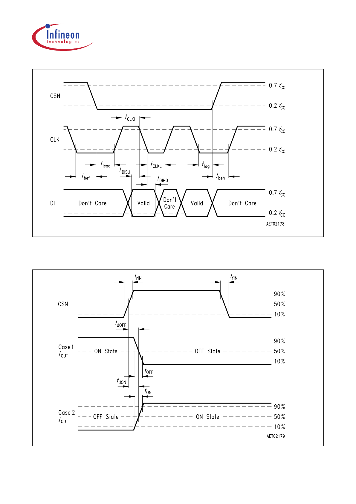
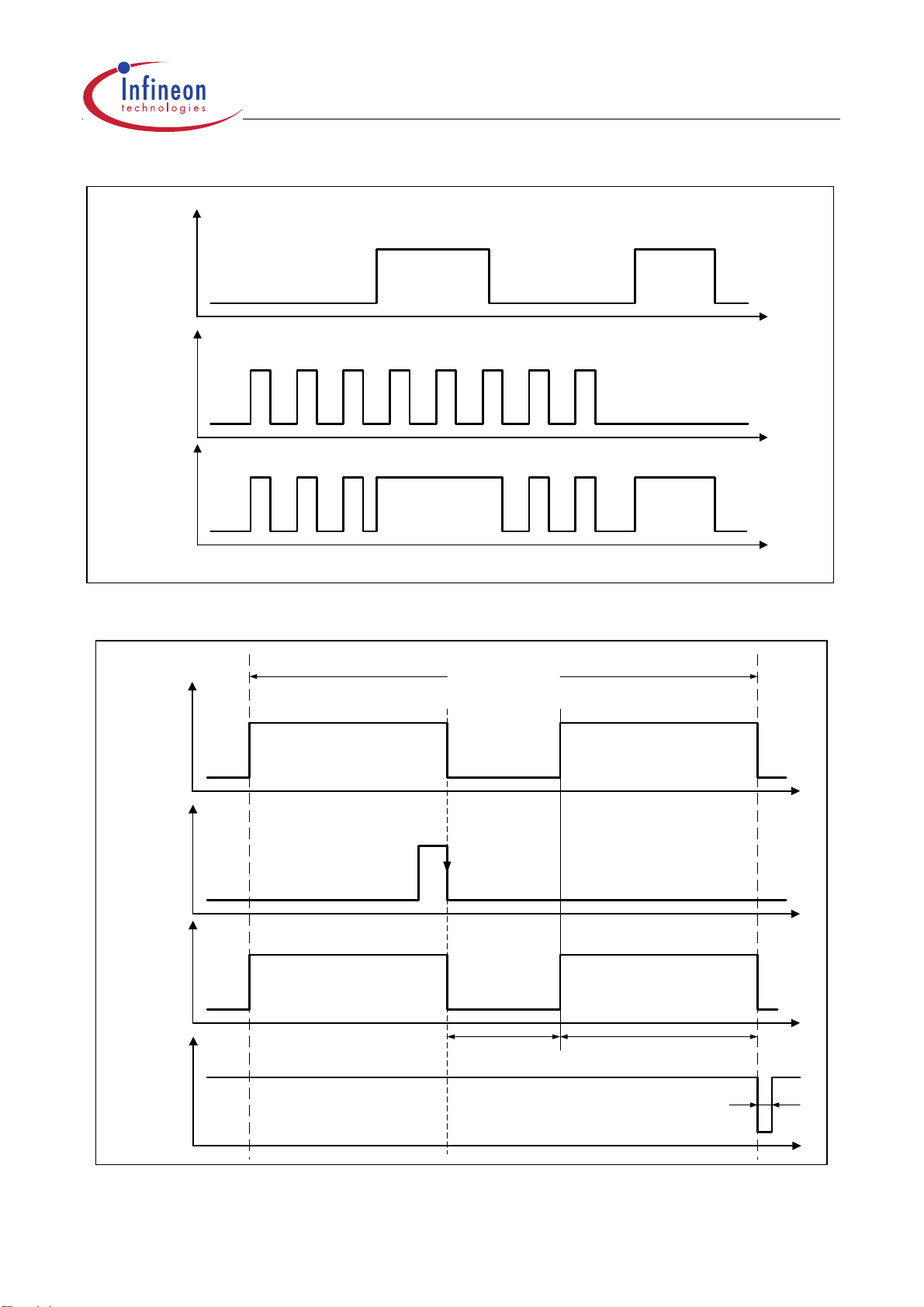
9Timing Diagrams
CSN High to Low & rising edge of CLK: DO is enabled. Status information is transfered to Output Shift Register
CSN
CSN Low to High: Data from Shift-Register is transfered to Output Power Switches
Target Datasheet TLE 6266
time
CLK
DI
DO
eg.
HS1
12345678910
0
0 141312
1
DI: Data will be accepted on the falling edge of CLK-Signal
__
0 141312
1
DO: State will change on the rising edge of CLK-Signal
__
432
5
previous Status
432
5
Figure 11 Data Transfer Timing
actual Data
76
8
76
8
109
109
11 12
11
11
13
14
15
15
15
10
new Data
01
++
actual Status
______________
0
1
actual Dataold Data
Version 1.06 41 2002-11-26
Target Datasheet TLE 6266
Figure 12 SPI-Input Timing
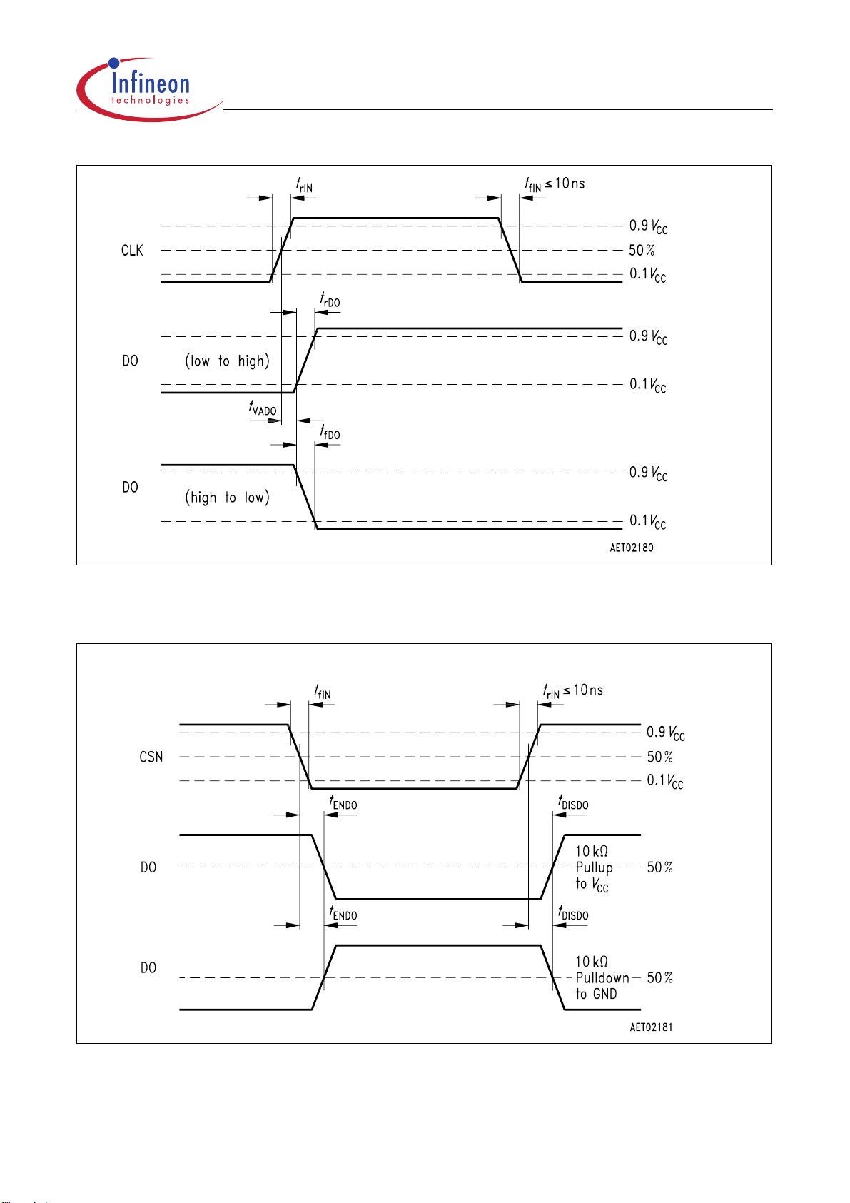
Figure 13 Turn OFF/ON Time
Version 1.06 42 2002-11-26
Target Datasheet TLE 6266
Figure 14 DO Valid Data Delay Time and Valid Time
Figure 15 DO Enable and Disable Time
Version 1.06 43 2002-11-26
SPI input
bit 1
Target Datasheet TLE 6266
H
L
PWM
(SPI input
bit 11 = H)
H
L
HS-
Switch1
ON
OFF
Figure 16 High Side Switch1 Timing Diagram
Cyclic
Wake
Vbat
stand-by
mode
ON
OFF
Cyclic Wake Mode
Cyclic HS OFFCyclic HS ON Cyclic HS ON
t
t
t
Vbat
stand-by
mode
t
WDR
t
t
t
PWM
HS-
Switch3
RO
H
L
ON
OFF
H
L
Correct
Trigger
Cyclic Wake
Time
No Trigger
Long Open Window t
LOW
Figure 17 Cyclic Wake Timing Diagram
Version 1.06 44 2002-11-26

Target Datasheet TLE 6266
t
WD
t
CW
closed window open window
Figure 18 Watchdog Timeout Definitions
t
CWtOW
WD
Trigger
t
CWtOW
tCW+t
OW
tCW+t
OW
t
OW
t
CWtOW
t
CWtOW
t / ms
t
CW
t
CW
t
CWtOW
t
Reset
WDR
Out
Watchdog
timer reset
normal
operation
timeout
(to long)
Figure 19 Watchdog Timing Diagram
normal
operation
timeout
(to short)
t
t
normal
operation
Version 1.06 45 2002-11-26

Target Datasheet TLE 6266
Vcc
WD
Trigger
Reset
Out
SPI output
bit 2
V
RT
V
ST
t
Watchdog
timer reset
RD
tCW+t
t
OW
WDR
t
start up start up
HIGH
LOW
activation by
microcontroller
t < t
RR
t
CWtOW
CWtOW
normal operation
t
RD
t
RR
undervoltage
t
SR
tCW+t
OW
t
t
t
t
Figure 20 Reset Timing Diagram
Current Consumption (typ.)
76
75
74
73
72
Current (µA)
71
70
69
10 100 1000 10000
48
Cyclic Wake Time (ms)
Current (µA ) typ.
"Static" Current
Figure 21 Current Consumption during Cyclic Wake Mode
Version 1.06 46 2002-11-26

Target Datasheet TLE 6266
5 V
C
1
C
2
C
1
13.5 V
100 nF
RxD
R
1
RTH
CANH
CANL
TxD
20 pF
CSN
DO
CLK
R
1
RTL
OUTL1
OUTL2
OUTH1
DI
PWM
RO
WK
OUTH2
V
OUTH3
CC
22 µF
+VS
GND
Figure 22 Timing Test Circuit
Version 1.06 47 2002-11-26

10 Application
Target Datasheet TLE 6266
V
bat
CAN bus
33 V
22 µF
68 nF
+V
S
CANH
CANL
RTH
RTL
OUTL2
OUTL1
OUTH3
OUTH2
OUTH1
TLE 6266 G
CSN
CLK
DI
DO
TxD
RxD
PWM
RO
Vcc
WK
GND
µC
e.g.
Infineon
C164
22 µF
GND
Figure 23 Application Circuit
Version 1.06 48 2002-11-26

11 Package Outlines
P-DSO-28-6
(Plastic Dual Small Outline Package)
Target Datasheet TLE 6266
Figure 24 The P-DSO-28-6 package
Sorts of Packing
Package outlines for tubes, trays etc. are contained in our
Data Book “Package Information”.
GPS05123
Dimensions in mm
Version 1.06 49 2002-11-26

Target Datasheet TLE 6266
Edition 1999-10-12
Published by Infineon Technologies AG
St.-Martin-Strasse 53
D-81541 München
© Infineon Technologies AG1999
All Rights Reserved.
Attention please!
The information herein is given to describe certain components and shall not be considered as warranted characteristics.
Terms of delivery and rights to technical change reserved.
We hereby disclaim any and all warranties, including but not limited to warranties of non-infringement, regarding
circuits, descriptions and charts stated herein.
Infineon Technologies is an approved CECC manufacturer.
Information
For further information on technology, delivery terms and conditions and prices please contact your nearest Infineon Technologies Office in Germany or our Infineon Technologies Representatives worldwide (see address list).
Warnings
Due to technical requirements components may contain dangerous substances. For information on the types in
question please contact your nearest Infineon Technologies Office.
Infineon Technologies Components may only be used in life-support devices or systems with the express written
approval of Infineon Technologies, if a failure of such components can reasonably be expected to cause the failure
of that life-support device or system, or to affect the safety or effectiveness of that device or system. Life support
devices or systems are intended to be implanted in the human body, or to support and/or maintain and sustain
and/or protect human life. If they fail, it is reasonable to assume that the health of the user or other persons may
be endangered.
Version 1.06 50 2002-11-26

Infineon goes for Business Excellence
“Business excellence means intelligent approaches and clearly
defined processes, which are both constantly under review and
ultimately lead to good operating results.
Better operating results and business excellence mean less
idleness and wastefulness for all of us, more professional
success, more accurate information, a better overview and,
thereby, less frustration and more satisfaction.”
Dr. Ulrich Schumacher
http://www.infineon.com
Published by Infineon Technologies AG
 Loading...