

现货库存、技术资料、百科信息、热点资讯,精彩尽在鼎好!
Data Sheet, Rev. 2.0, Jan. 2005
TLE 6258-2
LIN Transceiver
Automotive Power
Never stop thinking.

Edition 2005-01-13
Published by Infineon Technologies AG,
St.-Martin-Strasse 53,
81669 München, Germany
© Infineon Technologies AG 2004.
All Rights Reserved.
Attention please!
The information herein is given to descr ibe certain components and shall not be considere d as a guarant ee of
characteristics.
Terms of delivery and rights to technical change reserved.
We hereby disclaim any and all warranties, including but not limited to warranties of non-infringement, regarding
circuits, descriptions and charts stated herein.
Information
For further information on tech nology, delivery terms and conditions and prices please contact your nearest
Infineon Technologies Office (w ww.infineon.com).
Warnings
Due to technical requirements co mponents may contain dangerous substan ce s. For information on the t yp es in
question please contact your neares t Infineon Technologies Office.
Infineon Technologies Components may only be used in life-support devices or systems with the express written
approval of Infineon T echnologies, if a f ailure of such components can reasonably be expected to cause the failure
of that lif e -su pp o rt de vi ce o r system, or to aff ec t th e sa fety or effectiveness of th a t d evice or system. L i fe support
devices or systems are inten ded to be implante d in the human bod y, or to support and/or maintain and sustain
and/or protect human life. If they fail, it is reasonable to assume that the health of the user or other persons may
be endangered.
LIN Transceiver
Features
• Single-wire transceiver, suitable for LIN protocol
• Compatible to LIN specification 1.2, 1.3 and 2.0
• Compatible to ISO 9141 functions
• Transmission rate up to 20 kBaud
• Very low current consumption in stand-by mode
• Wake-up from Bus
• Short circuit proof to ground and battery
• Overtemperature protection
Description
TLE 6258-2
P-DSO-8-3, -6, -7, -8, -9
The single wire transceiver TLE 6258-2 is a monolithic integrated circuit in a P-DSO-8-3
package. It works as a n interfac e between the p rotocol controll er and the phy sical b us.
The TLE 6258-2 is especially suitable to drive the bus line in LIN systems in automotive
and industrial applications. Further it can be used in standard ISO9141 systems.
In order to reduce the current consumption the TLE 6258-2 offers a stand-by mode. A
wake-up caused by a message on the bus sets the RxD output low until th e device is
switched to normal operation mode.
The IC is based on the Smart Power Technology SPT
®
which allows bipolar and CMOS
control circuitry in accordance with DMOS power devices existing on the same
monolithic circuit.
The TLE 6258-2 is designed to withstand the severe conditions of automotive
applications.
Type Ordering Code Package
TLE 6258-2 G Q67006-A9695 P-DSO-8-3
Data Sheet 3 Rev. 2.0, 2005-01-13
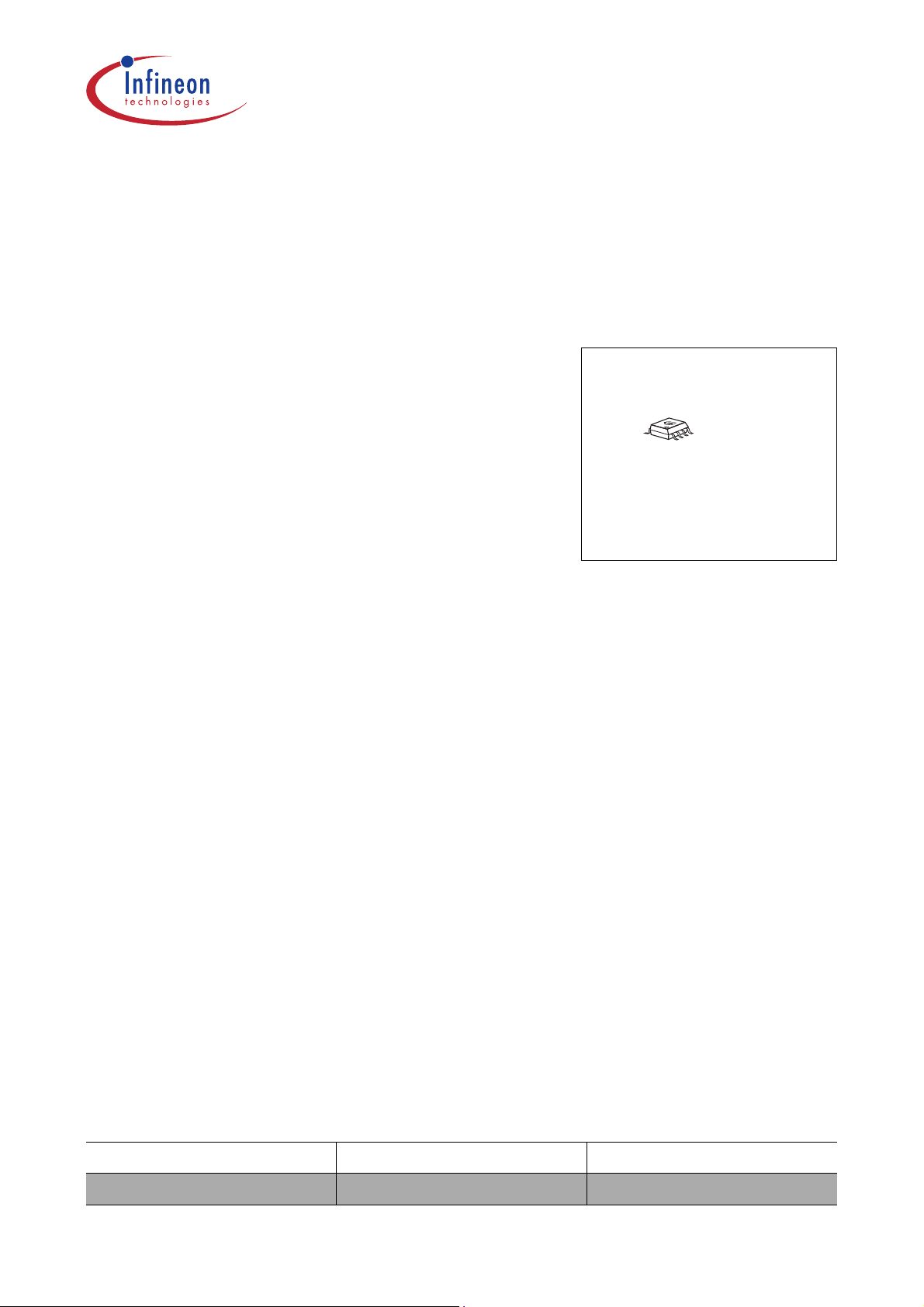
TLE 6258-2
TLE 6258-2 G
(P-DSO-8)
8
7
6
5
N.C.
V
S
Bus
GND
ENH
V
CC
1RxD
2
3
4TxD
AEP03406.VSD
Figure 1 Pin Configuration (top view)
Table 1 Pin Definitions and Functions
Pin No. Symbol Function
1RxDReceive data output; integrated pull-up, LOW in dominant state
2ENNEnable not input; integrated 30 kΩ pull-up, transceiver in normal
operation mode when LOW
3
V
CC
5 V supply input
4TxDTransmit data input; integrated pull-up, LOW in dominant state
5GNDGround
6BusBus output/input; internal 30 kΩ pull-up, LOW in dominant state
7
V
S
Battery supply input
8n.c.Not connected
Data Sheet 4 Rev. 2.0, 2005-01-13
TLE 6258-2
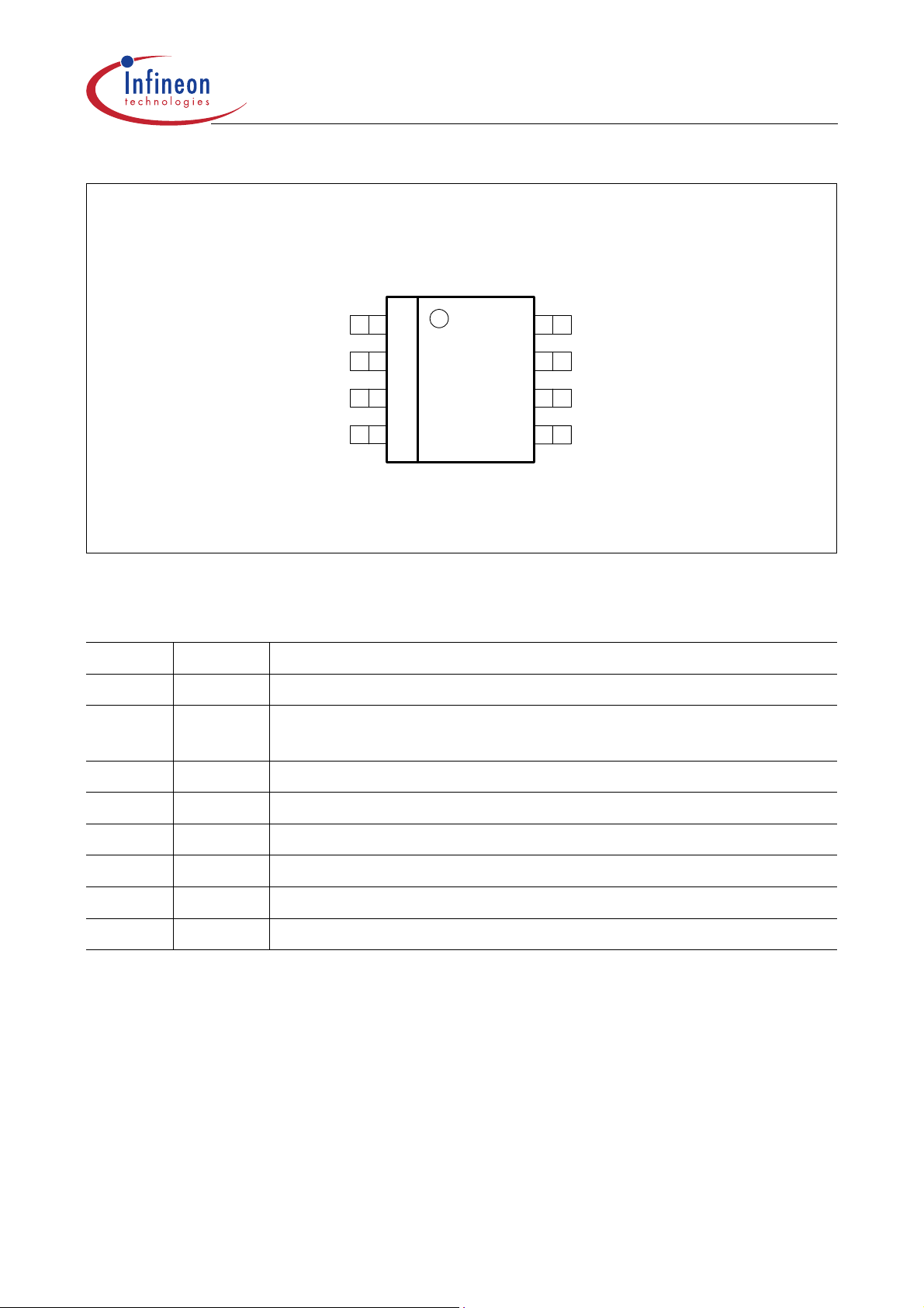
V
Bus
7
S
30 kΩ
6
Output
Stage
TLE 6258-2 G
30 kΩ
Mode Control
Driver
Temp.-
Protection
Receiver
3
2
4
1
5
V
CC
ENN
TxD
RxD
GND
Figure 2 Functional Block Diagram
AEB03405.VSD
Data Sheet 5 Rev. 2.0, 2005-01-13

Application Information
TLE 6258-2
RxD
Low
High
WAKE
Start Up
Power Up
V
CC
1)
ON or
3)
Off
Normal Mode
ENN
Low ON
HighENN
V
CC
ENN
ENN
High
LowENN
Low
Power-Up
Wake Up
t > t
Stand-by Mode
ENN
High
V
CC
ON or
Off
1) After wake-up via bus
3) After start up, V
CC
ON
TOAEA03451_1.VSD
Figure 3 State Diagram
For fail safe reasons the TLE 6258-2 has already a pull-up resistor of 30 kΩ
implemented. To achieve the required timings for the dominant to recessive transition of
the bus signal an additional external termination resistor of 1 kΩ is required. It is
recommended to place this resisto r in the mas ter node. To av oid reverse curren ts from
the bus line into the battery supply line in case of an unpowered node, it is recommended
to place a diode in series to the external pull-up. For small systems (low bus capacitance)
the EMC performance of the sys tem is supported by an additional capacitor of at le ast
1 nF in the master node (see Figure 6).
In order to reduce the current consumption the TLE 6258-2 offers a stand-by mode. This
mode is selected by switc hing the Enable Not (ENN) input high (see Figure 3). In the
stand-by mode a wake-up cau sed by a message on the bu s is indicated by s etting the
RxD output low. When entering the normal mode this wake-up flag is reset and the RxD
output is released to transmit the bus data.
Data Sheet 6 Rev. 2.0, 2005-01-13

TLE 6258-2
Table 2 Absolute Maximum Ratings
Parameter Symbol Limit Values Unit Remarks
Min. Max.
Voltages
Supply voltage
Battery supply voltage
Bus input voltage
Bus input voltage
Logic voltages at EN, TxD,
RxD
Electrostatic discharge
voltage at
V
, Bus
S
Electrostatic discharge
voltage
V
V
V
V
V
V
V
CC
S
bus
bus
I
ESD
ESD
-0.3 6 V –
-0.3 40 V –
-20 32 V –
-20 40 V t < 1 s
-0.3 VCC +
V0 V < VCC < 5.5 V
0.3
-4 4 kV human body model
(100 pF via 1.5 kΩ)
-2 2 kV human body model
(100 pF via 1.5 kΩ)
Temperatures
Junction temperature
T
j
-40 150 °C–
Note: Maximum ratings are abs olute ratings; exceeding any one of th ese values may
cause irreversible damage to the integrated circuit
.
Table 3 Operating Range
Parameter Symbol Limit Values Unit Remarks
Min. Max.
Supply voltage
Battery Supply Voltage
Junction temperature
V
V
T
CC
S
j
4.5 5.5 V –
635V–
-40 150 °C–
Thermal Shutdown (junction temperature)
Thermal shutdown temp.
Thermal shutdown hyst. ∆
T
jSD
150 170 190 °C
T –10–K
Thermal Resistances
Junction ambient
Data Sheet 7 Rev. 2.0, 2005-01-13
R
thj-a
–185K/W–

Table 4 Electrical Characteristics
TLE 6258-2
4.5 V <
V
< 5.5 V; 6.0 V < VS < 27 V; RL = 500 Ω; V
CC
ENN
< V
ENN,ON
; -40 °C < Tj < 125
°C; all voltages with respect to ground; positive current flowing into pin; unless otherwise
specified.
Parameter Symbol Limit Values Unit Remark
Min. Typ. Max.
Current Consumption
Current consumption
Current consumption I
Current consumption I
Current consumption I
Current consumption I
Current consumption
I
CC
S
CC
S
CC
I
S
– 0.4 0.7 mA recessive state;
V
= V
TxD
CC
– 0.5 1.0 mA recessive state;
V
= V
TxD
CC
– 0.4 0.8 mA dominant state;
V
= 0 V; without R
TxD
– 1.3 2.0 mA dominant state;
V
= 0 V; without R
TxD
0.4 0.7 mA power-up mode
– 0.5 1.0 mA power-up mod e,
V
= 0 V,
CC
V
= 13.5 V
S
L
L
Current consumption
Current consumption
I
CC
I
S
1310µA stand-by mode
–1840µA stand-by mode
Data Sheet 8 Rev. 2.0, 2005-01-13

Table 4 Electrical Characteristics (cont’d)
TLE 6258-2
4.5 V <
V
< 5.5 V; 6.0 V < VS < 27 V; RL = 500 Ω; V
CC
ENN
< V
ENN,ON
; -40 °C < Tj < 125
°C; all voltages with respect to ground; positive current flowing into pin; unless otherwise
specified.
Parameter Symbol Limit Values Unit Remark
Min. Typ. Max.
Enable Not Input (pin ENN)
HIGH level input voltage
threshold
LOW level input voltage
threshold
ENN input hysteresis
ENN pull-up resistance
V
ENN,off
V
ENN,on
V
ENN,hys
R
ENN
– 2.8 0.7 ×
V
CC
0.3 ×
V
CC
2.2 – V normal operation
V low power mode
300 600 900 mV –
15 30 60 kΩ –
mode
Receiver Output RxD
HIGH level output current
LOW level output current I
I
RD,H
RD,L
-1.2 -0.8 -0.5 mA VRD = 0.8 × V
0.5 0.8 1.2 mA VRD = 0.2 × V
CC
CC
Transmission Input TxD
HIGH level input voltage
threshold
TxD input hysteresis
LOW level input voltage
threshold
TxD pull-up current
V
TD,H
V
TD,hys
V
TD,L
I
TD
– 2.9 0.7 ×
V
CC
V recessive state
300 700 900 mV –
0.3 ×
V
CC
2.1 – V dominant state
-150 -110 -70 µA V
< 0.3 × V
TxD
CC
Data Sheet 9 Rev. 2.0, 2005-01-13

TLE 6258-2
Table 4 Electrical Characteristics (cont’d)
V
4.5 V <
< 5.5 V; 6.0 V < VS < 27 V; RL = 500 Ω; V
CC
°C; all voltages with respect to ground; positive current flowing into pin; unless otherwise
specified.
Parameter Symbol Limit Values Unit Remark
Min. Typ. Max.
Bus Receiver
ENN
< V
ENN,ON
; -40 °C < Tj < 125
Receiver threshold
voltage, recessive to
dominant edge
Receiver threshold
voltage, dominant to
recessive edge
Receiver hysteresis
Receiver threshold center
voltage
Input leakage current
Wake-up threshold
voltage
Bus Transmitter
Bus recessive output
voltage
V
bus,rd
V
bus,dr
V
bus,hys
V
bus,cnt
I
bus,lek
V
wake
V
bus,rec
0.44
×
– 0.56
0.02
×
0.475
×
V
V
V
S
S
S
0.48
V
×
S
V
×
S
0.04
V
×
S
0.5 ×
V
S
–V-8 V < V
0.6 ×
V
S
0.1 ×
V
S
0.525
×
V
V V
mV V
V
LIN2.0 table 3.1
S
-1 mA V
pull-up resistor as
specified in LIN2.0
0.40
×
0.9 ×
V
S
V
S
0.5 ×
V
S
0.6 ×
V
– V
V–
S
S
V V
bus,rec
bus,hys
bus,dom
= 0V, V
bus
= V
TxD
bus
< V
= V
CC
< V
< 20 V
bus
bus,rec
bat
bus,dom
-
= 12V,
Bus dominant output
voltage
Bus short circuit current
Leakage current
Bus pull-up resistance
Data Sheet 10 Rev. 2.0, 2005-01-13
V
bus,dom
I
bus,sc
I
bus,lk
R
bus
0–2VV
0–1.2V
40 100 150 mA V
= 0 V
TxD
7.3V<V
V
= 0 V
TxD
6V<V
S
bus,short
<27V
S
<7.3V
= 13.5 V
-1 - – mA VCC = 0 V, VS = 0 V,
V
= -8 V,
bus
–1020µA
V
= 0 V,
CC
V
= 13.5V,
S
V
= 20 V,
bus
20 30 47 kΩ –

Table 4 Electrical Characteristics (cont’d)
TLE 6258-2
4.5 V <
V
< 5.5 V; 6.0 V < VS < 27 V; RL = 500 Ω; V
CC
ENN
< V
ENN,ON
; -40 °C < Tj < 125
°C; all voltages with respect to ground; positive current flowing into pin; unless otherwise
specified.
Parameter Symbol Limit Values Unit Remark
Min. Typ. Max.
Dynamic Transceiver Characteristics
Falling edge slew rate
Rising edge slew rate S
Slope symmetry t
Propagation delay
S
bus(L)
bus(H)
slopesym
t
d(L),T
-3 -2.0 -1 V/µs
11.53V/µs
5-5µs t
60% > V
1 µs < (τ = R
V
= 5 V;
CC
= 13.5 V
V
S
1)
40% < V
1 µs < (τ = R
= 5 V;
V
CC
= 13.5 V
V
S
fslope
V
= 18 V
S
–13µs VCC = 5 V
- t
> 40%
bus
× C
L
< 60%
bus
× C
L
rslope
) < 5 µs;
BUS
) < 5 µs;
BUS
1)
TxD LOW to bus
Propagation delay
t
d(H),T
–13µs VCC = 5 V
TxD HIGH to bus
Propagation delay
bus dominant to RxD
LOW
Propagation delay
bus recessive to RxD
HIGH
Receiver delay symmetry
Transmitter delay
symmetry
Duty cycle D1 t
Duty cycle D2 t
t
d(L),R
t
d(H),R
t
sym,R
t
sym,T
duty1
duty2
–16µs VCC = 5 V;
C
= 20 pF
RxD
–16µs VCC = 5 V;
C
= 20 pF
RxD
-2 – 2 µs t
-2 – 2 µs t
0.396
––
––µs
0.581
µs
= t
sym,R
sym,T
duty cycle 1
TH
Rec
TH
Dom
= 7.0 … 18 V;
V
S
t
= 50 µs;
bit
D1 = t
duty cycle 2
TH
Rec
TH
Dom
VS = 7.6 … 18 V;
t
= 50 µs;
bit
D2 = t
d(L),R
= t
d(L),T
(max) = 0.744 × VS;
(max) = 0.581 × VS;
bus_rec(min)
(max) = 0.422× VS;
(max) = 0.264 × V
bus_rec(max)
- t
d(H),R
- t
d(H),T
1)
/2 t
;
bit
1)
S
/2 t
;
bit
Data Sheet 11 Rev. 2.0, 2005-01-13

Table 4 Electrical Characteristics (cont’d)
TLE 6258-2
4.5 V <
V
< 5.5 V; 6.0 V < VS < 27 V; RL = 500 Ω; V
CC
ENN
< V
ENN,ON
; -40 °C < Tj < 125
°C; all voltages with respect to ground; positive current flowing into pin; unless otherwise
specified.
Parameter Symbol Limit Values Unit Remark
Min. Typ. Max.
Wake-up delay time t
Delay time for mode
wake
t
snorm
30 100 150 µs Tj < 125 °C
170 µs
T
< 150 °C
j
50 µs
change
1) Bus load conditions concerning LIN spec 2.0 C
bus
, R
= 1 nF, 1 kΩ / 6.8 nF, 660 Ω / 10 nF, 500 Ω
bus
Data Sheet 12 Rev. 2.0, 2005-01-13

TLE 6258-2
1 kΩ
C
Bus
Figure 4 Test Circuits
V
TxD
V
CC
100 nF
V
S
Bus
GND
ENN
TxD
RxD
V
CC
20 pF
100 nF
AEA03408.VSD
GND
t
V
Bus
V
S
d(L),T
V
Bus,rd
t
d(H),T
GND
t
d(L),R
V
RxD
V
CC
GND
t
d(L),TR
0.3 x V
CC
t
d(H),TR
Figure 5 Timing Diagram for Dynamic Characteristics
V
t
Bus,dr
d(H),R
0.7 x V
AET03409.VSD
t
t
CC
t
Data Sheet 13 Rev. 2.0, 2005-01-13

Application
V
LIN Bus
Bat
Master Node
1 kΩ
V
100
nF
TLE 6258-2 G
S
ENN
RxD
TxD
TLE 6258-2
µP
+
Slave Node
22
µF
V
100
nF
V
100
nF
Bus
V
GND
I
e. g. TLE 4278
GND
TLE 6258-2 G
S
ENN
RxD
Bus
TxD
V
GND
V
CC
CC
100
nF
100
nF
GND
5 V
Q
+
22 µF
ECU 1
µP
100
nF
100
nF
GND
V
I
+
22
µF
e. g. TLE 4278
100
nF
GND
V
Q
5 V
+
22 µF
ECU X
AEA03404.VSD
Figure 6 Application Circuit
Data Sheet 14 Rev. 2.0, 2005-01-13

Package Outlines
0.1 MIN.
(1.5)
1.75 MAX.
0.33
±0.08
x 45˚
4
-0.2
1)
1
+0.05
-0.0
0.2
TLE 6258-2
MAX.8˚
0.41
1.27
+0.1
-0.05
0.1
0.2MA
8
5
C
x8
C
±0.2
6
Index
Marking
4
1
A
1)
5
-0.2
Index Marking (Chamfer)
1)
Does not include plastic or metal protrusion of 0.15 max. per side
Figure 7 P-DSO-8-3 (Plastic Dual Small Outline)
0.64
±0.25
GPS09032
You can find all of our packages, sorts of packing and others in our
Infineon Internet Page “Products”: http://www.infineon.com/products.
SMD = Surface Mounted Device
Dimensions in mm
Data Sheet 15 Rev. 2.0, 2005-01-13
 Loading...