

Page 1
现货库存、技术资料、百科信息、热点资讯,精彩尽在鼎好!
Single Wire CAN-Transceiver
Final Data Sheet
1Features
• Single wire transceiver for up to 33 kBit/s bus speed
• Compatibel to GM LAN Standard GMW 3089 - V1.26
• Excellent EMC performance
• High speed mode for up to 100 kBit/s bus speed
• Ambient operation range
• Supply voltage operation range 5.5 V to 28 V
•Typ. 30 µA total current consumption in sleep mode
• 4 kV ESD protection
• Short circuit and overtemperature protected
• Input bilevel feature for wake-up detection
• Output bilevel feature for wake up call
• Loss of Ground protection
• Bus dominant timeout feature
• Programmable slewrate
– 40 °C to 125 °C
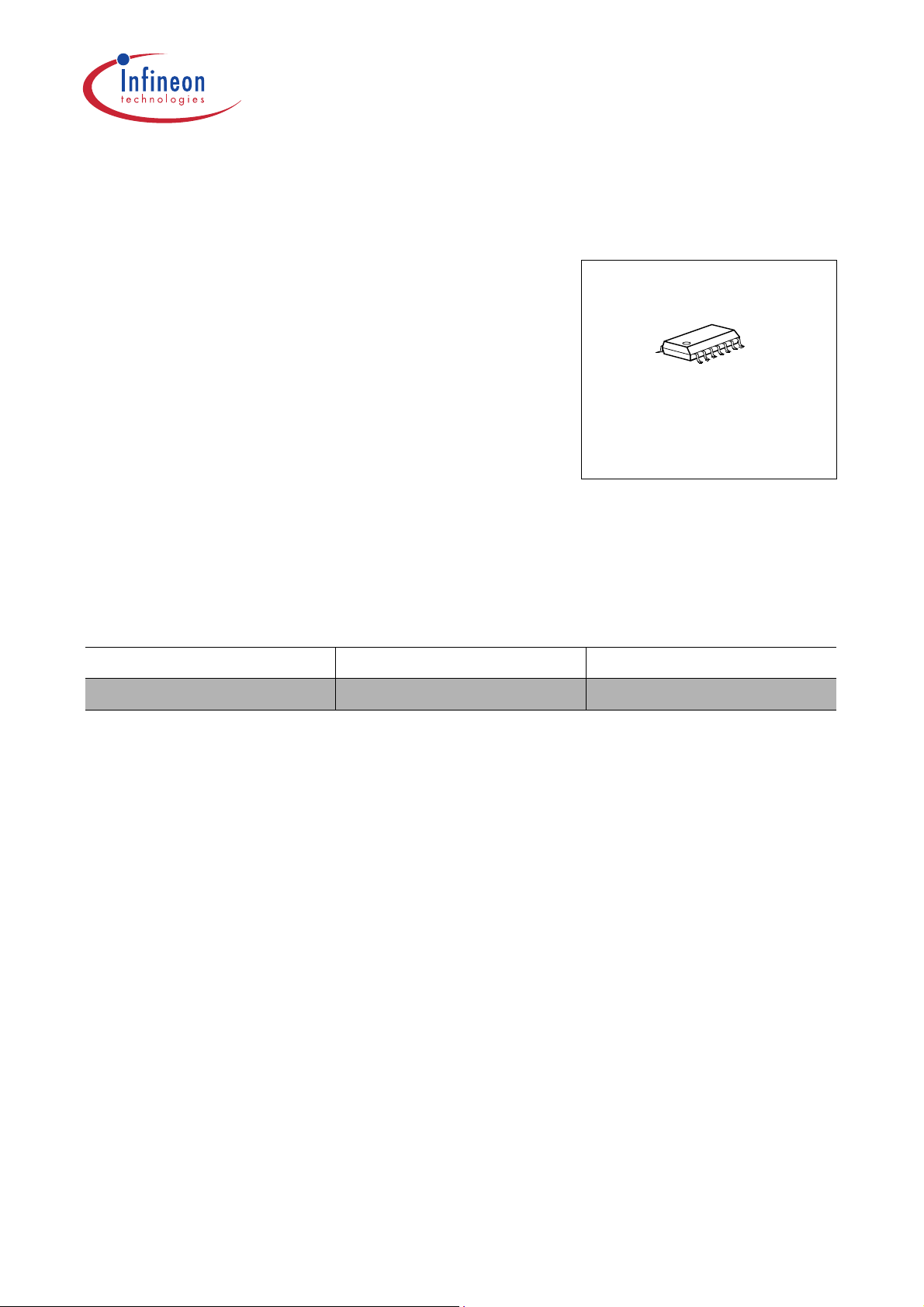
TLE 6255 G
P-DSO-14-8; -9
Type Ordering Code Package
TLE 6255 G Q67006-A9352 P-DSO-14-9 (SMD)
2 Description
The TLE 6255 G is a special featured low speed transceiver for use in single wire
applications.
The device is primarily designed for use in single wire CAN systems operating with
various CSMA/CR (carrier sense multiple access/collision resolution) protocols such as
the BOSCH Controller Area Network (CAN).
The normal communication bitrate in CAN-systems is up to 33 kBit/s. For software or
diagnostic data download a high speed mode is offered that allows transmission rates
up to 100 kBit/s.
With many integrated features such as slewrate controlled output, loss of ground circuit,
bi-level wake-up and sleep mode for low power consumption the TLE 6255 G is
optimized for use in automotive applications.
The device is based on Smart Power Technology SPT
control circuitry to be integrated with DMOS power devices on the same monolithic
®
which allows bipolar and CMOS
circuitry.
Additional features like short circuit and overtemperature protection, over- and
undervoltage lockout are integrated. To enhance the reliability and robustness of the
TLE 6255 G the enhanced power SO-14 package is used in order to provide high
thermal capacity and low thermal resistance.
Data Sheet Rev. 2.5 1 2003-11-27
Page 2
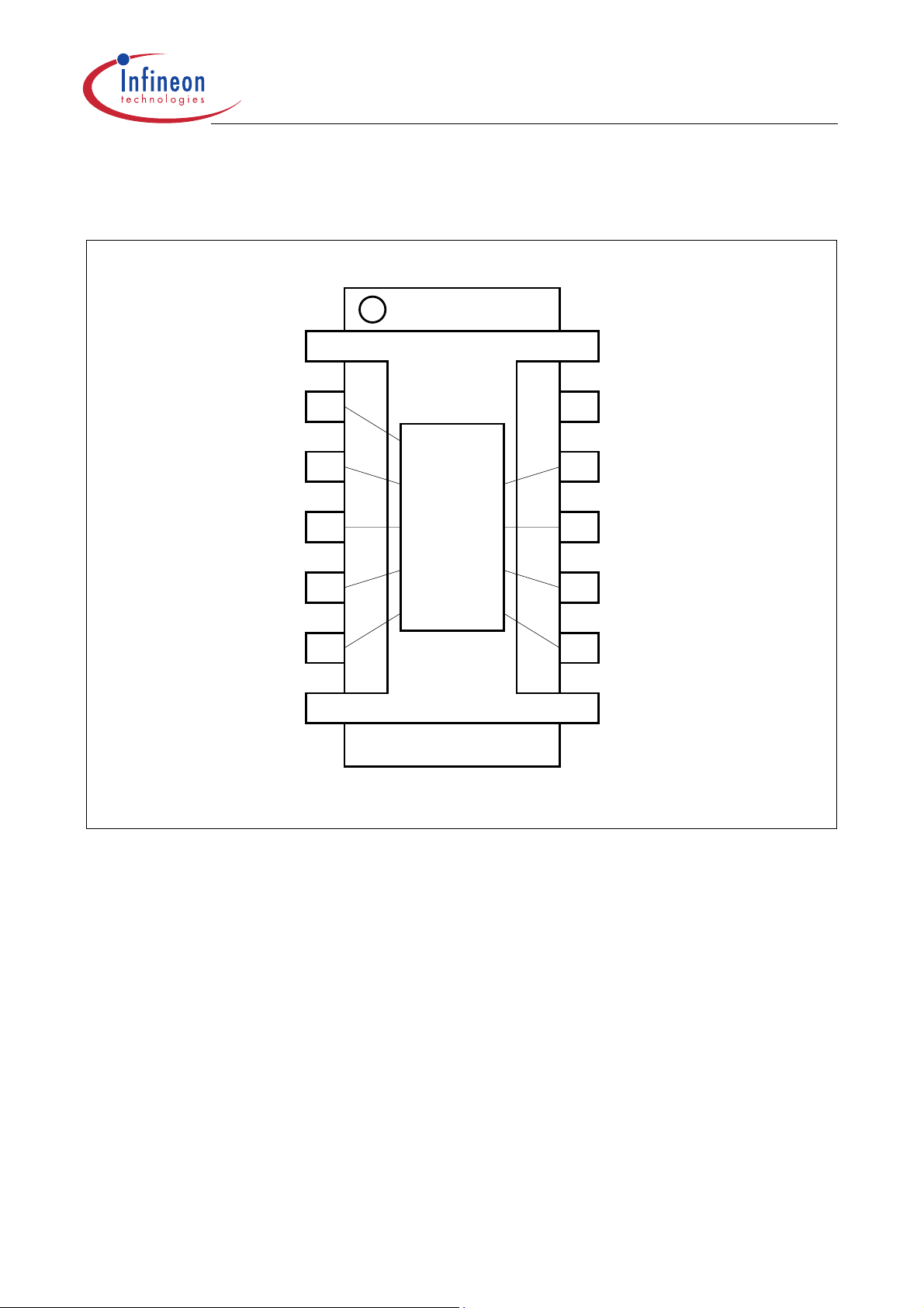
3 Pin Configuration
(top view)
TLE 6255 G
GND
TxD
M0
M1
RxD
V
CC
GND
1
2
3
4
5
6
7
Leadframe
Chip
AEP02568
14
13
12
11
10
9
8
GND
N.C.
CANH
LOAD
V
batt
RSL
GND
Figure 1 Pin Configuration
RxD = H indicates a bus recessive state, RxD = L a bus normal or high voltage dominant
state.
Data Sheet Rev. 2.5 2 2003-11-27
Page 3
TLE 6255 G
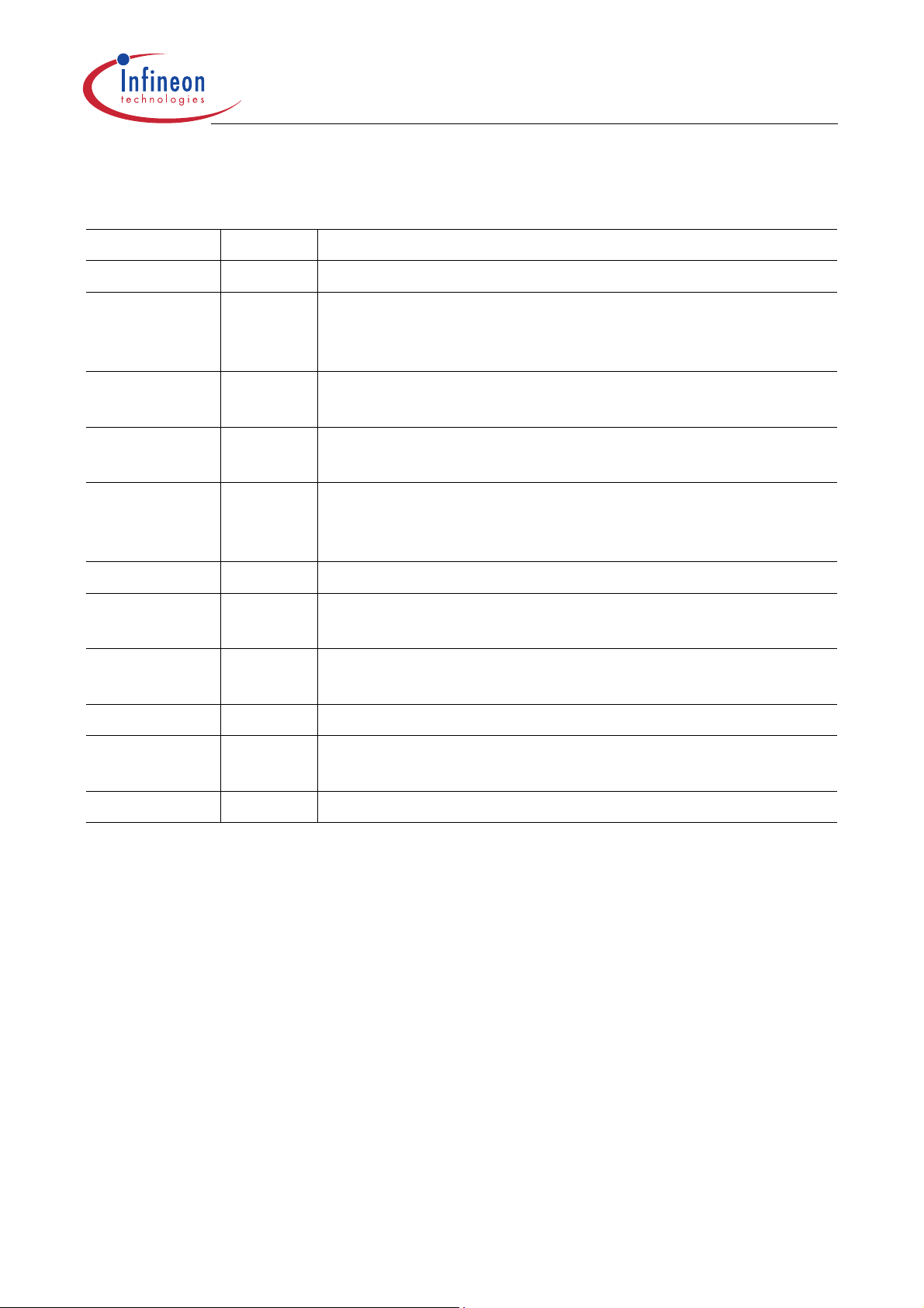
4 Pin Definitions and Functions
Pin No. Symbol Function
1, 7, 8, 14 GND Ground; internally connected to leadframe
2TxDTransceive-Input; low active, logic command to transmit
on the single wire CAN bus; inverting: TxD = low causes
CANH = dominant (high level); internal 10 kΩ pull up
3M0Mode-Input 0; to program the device operating mode;
internal pull down
4M1Mode-Input 1; to program the device operating mode;
internal pull down
5RxDReceive-Output; open drain, logic data as sensed on the
single wire CAN bus; inverting (RxD = L when CANH is
dominant)
6
9RSLSlewrate-Program-Input; an external resistor to
V
CC
Supply Voltage; input for 5 V logic supply voltage
V
CC
on
this pin is required to program the bus output slewrate
10
V
batt
Battery Supply Voltage; external blocking capacitor
necessary (see application circuit)
11 LOAD Unit-Load Resistor Input; internal termination to GND
12 CANH CAN Bus Input/Output; single wire bus input and output;
short circuit protected
13 N.C. not connected
Data Sheet Rev. 2.5 3 2003-11-27
Page 4
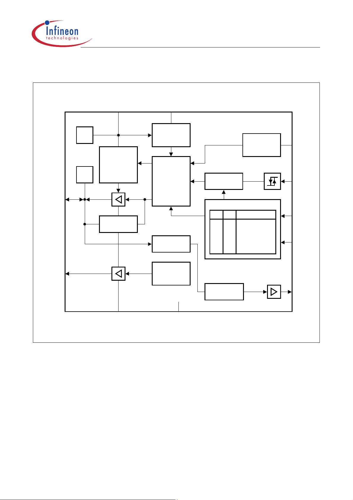
5 Block Diagram
TLE 6255 G
CANH
LOAD
12
11
4 kV
ESD
4 kV
ESD
V
Batt
10
Protection
and
Startup-
Control
Driver
Feedback-
Loop
Load
Driver
V
CC
6
Biasing
OVLO
UVLO
Wave-
Shape-
Circuit
Input
Filter
Loss of
Ground
Control
Converter
Time Out
Circuit
Mode-Logic
M1 M0 Mode
L L Sleep
HL High-Speed
LH Wake-up Call
HH Normal
Receive
Comp
TLE 6255G
Voltage
Current
BUF
9
2
3
4
5
RSL
TxD
M0
M1
RxD
1, 7, 8, 14
GND
13
N.C.
AEB02565
Figure 2 Block Diagram
Data Sheet Rev. 2.5 4 2003-11-27
Page 5
TLE 6255 G
6 Functional Description and Application Hints
6.1 Mode Control
By use of the two mode control pins M0 and M1 the transceiver can be set in the
following modes.
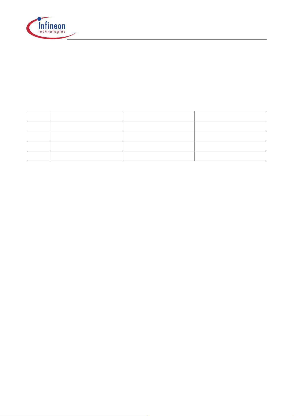
Table 1 Transceiver Modes
#M0M1Mode
1 Low Low Sleep mode
2 High Low High speed mode
3 Low High Wake-up call
4 High High Normal mode
Sleep-Mode
In the sleep mode the total current consumption of the TLE 6255 G is reduced to typically
30 µA. Nodes not set to sleep mode can communicate without disturbing ECUs that are
already set to sleep mode. To achieve a wake-up via the CAN bus a high voltage level
message (wake-up call) is necessary. Only high voltage level messages are reported to
the RxD pin in sleep mode. A wake-up from sleep mode of the transceiver itself has to
be done by setting the control inputs M0 and M1. If there is no modification on the mode
inputs the device remains in sleep mode after the wake-up signal is removed from the
bus.
The transceiver’s loss of ground protection circuit connection to ground is not interrupted
when in the sleep mode.
High-Speed-Mode
The high-speed mode can be used for software or diagnostic data download with bitrates
up to 100 kBit/s. Therefore the slewrate control feature is deactivated to achieve the
required timings. Further an additional external resistor of 100 Ω from CANH to GND is
necessary in this mode.
Wakeup-Call Mode
In this mode the TLE 6255 G sends the message to be transmitted as a high voltage
wake-up message.
The bus includes a special node wake up capability which allows normal communication
to take place among some nodes while leaving the other nodes in an undisturbed sleep
state. This is accomplished by controlling the level of the signal voltages such that all
nodes must wake up when they receive a higher voltage message signal waveform.
Communication at the lower, normal voltage levels shall not disturb the sleeping nodes
(
V
>9V).
batt
Data Sheet Rev. 2.5 5 2003-11-27
Page 6

TLE 6255 G
Normal Mode
In the normal mode the TLE 6255 G sends a normal voltage message waveform on the
bus. It is possible to run the transceiver up to transmission rates of 33 kBits/s in this
mode.
The waveform as well as the slew rate of the rising edge (recessive to dominant
transition) are controlled by the internal active wave shaping circuit to minimize EME
(electromagnetic emission). For the same reason waveform trailing edge control is
required to assure that high frequency content is minimized at the beginning of the
downward voltage slope (dominant to recessive transition). The remaining fall time
occurs after the bus is inactive with drivers off and is determined by the RC time constant
of the total bus load.
6.2 Slew-Rate Control
The CANH output voltage and current is controlled by an internal waveshaping circuit.
For optimized adjusting of the slew rate to the system timing, the slew rate is
programmable by an external resistor connected from pin RSL to
R
the correlation of the slew rate to the resistor
RSL
.
V
. Figure 4 shows
CC
6.3 Transmitter
The TLE 6255 G contains a high current fully short circuit and overtemperature protected
highside-driver (pin CANH). To minimize spectral content the CANH-output waveform is
controlled.
Logic low (TxD = L) on pin TxD will command the output stage to switch to dominant high
potential; TxD = H to recessive low on the bus.
To avoid the bus to be blocked by a permanent dominant TxD input signal, the
TLE 6255 G incorporates a timeout feature. In case of TxD = L for longer than the
internal fixed timeout the CANH output is switched off automatically. The timeout is
resetted by a H-signal at TxD without a delay.
The loss of an ECU ground may cause the ECU to source current through the various
ECU circuits to the communications bus instead of to the vehicle system ground.
Therefore the unit-load resistor of any ECU is connected to the LOAD-pin. The
TLE 6255 G incorporates a reverse protected switch from LOAD to ground potential.
This switch is automatically switched off in a loss of ground state.
6.4 Receiver
In normal, high speed and wakeup-mode all data on the bus is sensed by the receive
comparator and transmitted to the RxD output. In sleep mode no normal level data is
detected. The receiver threshold is set to the wake-up level. So a wake-up interrupt is
sent only in case of a wake-up call on the bus. An internal fixed filter improves the EMC
susceptibility.
Data Sheet Rev. 2.5 6 2003-11-27
Page 7

TLE 6255 G
6.5 Unit Load Resistor
The TLE 6255 covers the specification GMW 3089 V1.26 or the so called first generation
of SW CAN. GM decided to design a second generation of SW CAN, which is defined in
the specification GMW 3089 V2.0. This led to some differences in the electrical
characteristics(GND shift, time constants, etc.) and also in the pinout (pin 9 is used to
control a voltage regulator).
It must be pointed out, that GMW 3089 V1.26 defines a unit load resistance of:
R
= 8,999 to 9,126 kOhm
UL
With this R
of this range are not a subject to GMW 3089 V1.26!
The loss of ground circuit is not specified to function when the load resistor is out of the
8.999-9.126 kohm range!
, the TLE 6255 complies to the GMW 3089 V1.26 specification. Values out
UL
Data Sheet Rev. 2.5 7 2003-11-27
Page 8

TLE 6255 G
7 Absolute Maximum Ratings
Parameter Symbol Limit Values Unit Remarks
min. max.
Voltages
Supply voltage
CAN bus input/output voltage
Load voltage
Logic supply voltage
Logic voltages
(
V
RxD
; V
; VM0; VM1; V
TxD
RSL
)
V
V
V
V
V
batt
CANH
LOAD
CC
logic
– 0.3 40 V –
– 28 28 V –
– 28 28 V –
– 0.3 7 V –
– 0.3 7 V –
Currents
CAN Bus current
Load current
I
CANH
I
LOAD
– – mA internally limited
– – mA internally limited
ESD-Protection (Human Body Model; According to MIL STD 833 D)
Pin CANH, V
Other pins
batt
V
V
ESD
ESD
– 4000 4000 V –
– 2000 2000 V –
Temperatures
Junction temperature T
Junction temperature
Junction temperature
Storage temperature
j
T
j
T
j
T
stg
– 40 150 °C–
–175°C t < 1000 h
–200°C t <10h
– 50 150 °C–
Thermal Resistances
Junction to pin R
Junction ambient
R
thj-pin
thj-a
– 40 K/W junction to pin 1
–65K/W–
Note: Maximum ratings are absolute ratings; exceeding any one of these values may
cause irreversible damage to the integrated circuit.
Data Sheet Rev. 2.5 8 2003-11-27
Page 9

8 Operating Range
Parameter Symbol Limit Values Unit Remarks
min. max.
TLE 6255 G
Supply voltage
V
Supply voltage increasing V
Supply voltage decreasing
Logic supply voltage
Logic supply voltage;
V
V
V
increasing
Logic supply voltage;
V
decreasing
Junction temperature
RSL resistance
T
R
Thermal Shutdown
Thermal shutdown junction
T
temperature
batt
batt
batt
CC
CC
CC
j
RSL
jSD
V
UVOFF
– 0.3 V
– 0.3 V
V
POROF
– 0.3 V
– 0.3 V
28 V After V
V
UV ON
UV ON
UV OFF
V Outputs in tristate
V Outputs in tristate
5.5 V After V
V
PORON
PORON
POROF
V Outputs in tristate
V Outputs in tristate
– 40 150 °C–
35 200 kΩ –
150 200 °C–
rising above
batt
rising above
CC
Thermal switch-on junction
temperature
T
jSO
120 170 °C temperature hysteresis
∆T = 30° K (typ.)
Data Sheet Rev. 2.5 9 2003-11-27
Page 10

9 Electrical Characteristics
TLE 6255 G
5.5 V <
R
UL
V
< 16 V; 4.75 V < V
batt
< 5.25 V; – 40 °C<Tj<150 °C; M0 = M1 = H;
CC
= 9.1 kΩ (connected between CANH and LOAD); R
=39kΩ; all voltages with
RSL
respect to ground; positive current defined flowing into pin; unless otherwise specified
Parameter Sym-
bol
Limit Values Unit Test Condition
min. typ. max.
Current Consumption
Supply current at
batt
I
batt
–2040µAM0=M1=L;
V
;
sleep mode
Supply current at
CC
I
CC
–1030µAM0=M1=L;
V
;
sleep mode
Supply current at
Supply current at
Supply current at
Supply current at
Supply current at
V
battIbatt
V
battIbatt
V
battIbatt
V
battIbatt
V
CCICC
–36mATxD=L
–1.53mATxD=H
–59mATxD=L; M0=L
– 4 6 mA TxD=H; M0=L
– 3 5 mA TxD = H or L;
M0 = H or L
Over- and Under Voltage Lockout
UV Switch ON voltage
UV Switch OFF voltage
UV ON/OFF
V
UVON
V
UVOFF
V
UVHY
–5.25.6VV
4.00 4.6 5.1 V V
–0.6–VV
Hysteresis
OV Switch OFF
V
OVOFF
30 33 38 V V
voltage
OV Switch ON voltage
OV ON/OFF
V
OVON
V
OVHY
28 32 36 V V
0.2 2 – V V
Hysteresis
increasing;
batt
V
= 5 V
CC
decreasing;
batt
V
=5 V
CC
– V
UVON
increasing
batt
decreasing
batt
OVOFF
– V
UVOFF
OVON
Data Sheet Rev. 2.5 10 2003-11-27
Page 11

TLE 6255 G
V
5.5 V <
R
= 9.1 kΩ (connected between CANH and LOAD); R
UL
< 16 V; 4.75 V < V
batt
respect to ground; positive current defined flowing into pin; unless otherwise specified
< 5.25 V; – 40 °C<Tj<150 °C; M0 = M1 = H;
CC
=39kΩ; all voltages with
RSL
Parameter Sym-
bol
Power ON/OFF Reset at V
Power ON Reset
V
PORON
CC
voltage
Power OFF Reset
V
POROF
voltage
POR ON/OFF
V
PORHY
Hysteresis
Transceive Input TxD
H-input voltage
V
TxDH
threshold
L-input voltage
V
TxDL
threshold
Limit Values Unit Test Condition
min. typ. max.
4.00 4.25 4.50 V VCC increasing
3.50 3.75 4.00 V VCC decreasing
0.1 0.5 – V V
–2.60.7×
V
CC
0.3 ×
V
CC
2.4 – V –
V–
PORON
– V
POROF
Hysteresis of input
voltage
Pull up current
Timeout reaction time
Receive Output RxD
Output leakage current I
Output low voltage
level
Falltime
V
TxDHY
I
TxD
t
TOR
RxDLK
V
RxDL
t
FRxD
50 200 500 mV –
–20 –10 –5 µA0 V<V
51030ms–
– 2 0 10 µA V
–0.20.4VI
–80200nsC
=5 V
RxD
=2 mA
RxDL
= 25 pF to GND
RxD
TxD
<4 V
Data Sheet Rev. 2.5 11 2003-11-27
Page 12

TLE 6255 G
5.5 V <
R
UL
V
< 16 V; 4.75 V < V
batt
< 5.25 V; – 40 °C<Tj<150 °C; M0 = M1 = H;
CC
= 9.1 kΩ (connected between CANH and LOAD); R
=39kΩ; all voltages with
RSL
respect to ground; positive current defined flowing into pin; unless otherwise specified
Parameter Sym-
bol
Limit Values Unit Test Condition
min. typ. max.
Mode Input M0 and M1
H-input voltage
threshold
L-input voltage
threshold
Hysteresis of input
V
M0,1H
V
M0,1L
V
M0,1HY
–2.60.7×
V
CC
0.3 ×
V
CC
2.4 – V –
V–
50 200 500 mV –
voltage
Pull down current
I
M0,1
52050µA1V<V
M0,1
<5V
Mode Change Delaytimes
Normal to high-speed t
Normal to wakeup call
Normal to sleep
Sleep to normal
Slewrate Input RSL
Output voltage
DNH
t
DNW
t
DNS
t
DSN
V
RSL
–530µs M1 H to L;
(not tested, specified by
design)
–530µs M0 H to L
(not tested, specified by
design)
–5500µs M0 and M1 H to L
(not tested, specified by
design)
–550µs M0 and M1 L to H
(not tested, specified by
design)
2.5 3 3.5 V I
=100 µA
RSL
Data Sheet Rev. 2.5 12 2003-11-27
Page 13

TLE 6255 G
5.5 V <
R
UL
V
< 16 V; 4.75 V < V
batt
< 5.25 V; – 40 °C<Tj<150 °C; M0 = M1 = H;
CC
= 9.1 kΩ (connected between CANH and LOAD); R
=39kΩ; all voltages with
RSL
respect to ground; positive current defined flowing into pin; unless otherwise specified
Parameter Sym-
bol
Limit Values Unit Test Condition
min. typ. max.
CANH as Bus Input / Receiver
Wake up offset
threshold
Wake up fixed
threshold
Wakeup dead time
Wakeup minimal pulse
V
IHWUOVbatt
V
IHWUF
t
DWU
t
WUMIN
–
– V
4.30
6.15 7.1 8.10 V V
batt
3.25
–
V V
batt
see note; see Figure 8
batt
see note; see Figure 8
10 21 50 µs–
1510µs–
= 8 V
= 14 V
time
Receive threshold; in
V
IH
1.8 2 2.2 V 6 V < V
batt
<16V
normal, high-speed
and wake-up mode
Receive hysteresis
Receive propagation
time
Receive propagation
time; high speed
Receive propagation
time
Receive propagation
time; high speed
Receive blanking time
after CANH H to L
transition
V
t
CRF
t
CRF
t
CRR
t
CRR
t
CRB
RHY
50 80 200 mV –
0.05 0.3 1 µs V
>(VIH+ 0.8 V) to
CANH
RxD = L; 6 V <
0.05 0.25 0.5 µs V
>(VIH+ 0.8 V) to
CANH
RxD = L; M1 = L;
6V<
T
0.05 0.3 1 µs V
RxD = H;
6V<
0.05 0.25 0.5 µs V
RxD = H;
V
<16V;
batt
< 125 °C
j
< (VIH– 0.8 V) to
CANH
R
RxD
V
<16V
batt
< (VIH– 0.8 V) to
CANH
R
RxD
M1 = L; 6 V <
T
< 125 °C
j
1.5 3.0 5.0 µs see Figure 7
V
<16 V
batt
=2.4kΩ
=2.4kΩ
V
<16V;
batt
Note: The device will send a wake up call to the microcontroller at the minimum of
V
Data Sheet Rev. 2.5 13 2003-11-27
IHWUO
or V
IHWUF
.
Page 14

TLE 6255 G
V
5.5 V <
R
= 9.1 kΩ (connected between CANH and LOAD); R
UL
< 16 V; 4.75 V < V
batt
respect to ground; positive current defined flowing into pin; unless otherwise specified
< 5.25 V; – 40 °C<Tj<150 °C; M0 = M1 = H;
CC
=39kΩ; all voltages with
RSL
Parameter Sym-
bol
min. typ. max.
CANH as Bus Output / Transmitter
Offset wakeup output
high voltage
Fixed wakeup output
V
OHWUOVbatt
V
OHWUF
1.5
9.7 – 12 V 220 Ω < RUL<9.1kΩ
high voltage
Bus output high
V
OH
3.60 4.0 4.55 V 100 Ω < RUL<9.1 kΩ
voltage; normal and
high speed
Bus output current limit
Bus output leakage
I
OLI
I
OLK
200 250 350 mA TxD = L; V
– 10 – 200 µATxD=H; Tj< 125 °C;
current
Limit Values Unit Test Condition
–
– V
batt
V220Ω < RUL<9.1kΩ;
TxD = L; M0 = L;
V
6V<
batt
<V
OHWUF
TxD = L; M0 = L
V
OHWUF
< V
batt
TxD = L; 6 V <
CANH
V
–28V<V
batt
V
–1V
batt
<16V
V
batt
=0 V
CANH
<16V
<
Bus output leakage
current (loss of ground)
Slew rate rising edge,
normal mode
Slew rate rising edge,
wake-up mode
Slew rate rising edge;
high speed;
Transmit propagation
time; normal mode
Transmit propagation
time; wake-up mode
I
OLK
S
CANH
S
CANH
S
CANH
t
TCF
t
TCF
– 50 – 200 µA0V<V
V
–28 V<V
batt
V
–1 V
batt
–2.0–V/µs20%<V
–4.0–V/µs20%<V
M0 = L;
51625V/µs20%<V
M1 = L;
< V
batt
CANH
CANH
V
batt
CANH
T
< 125 °C
j
UVOFF
CANH
< 80%
< 80%
=12V
< 80%
256µsTxD=(HtoL) to
V
=(VIH+0.8V)
CANH
1.0 µs < τ < 3.6 µs;
154µsTxD=(HtoL) to
V
M0 = L;
=(VIH+ 0.8 V);
CANH
V
batt
= 12 V;
1.0 µs < τ < 3.6 µs
;
<
Data Sheet Rev. 2.5 14 2003-11-27
Page 15

TLE 6255 G
5.5 V <
R
UL
V
< 16 V; 4.75 V < V
batt
< 5.25 V; – 40 °C<Tj<150 °C; M0 = M1 = H;
CC
= 9.1 kΩ (connected between CANH and LOAD); R
=39kΩ; all voltages with
RSL
respect to ground; positive current defined flowing into pin; unless otherwise specified
Parameter Sym-
bol
Transmit propagation
t
TCF
time; high speed mode
Limit Values Unit Test Condition
min. typ. max.
–0.51.5µsTxD=(HtoL) to
V
=(VIH+ 0.8 V);
CANH
M1 = L; τ < 1 µs;
T
< 125 °C
j
Transmit propagation
time; normal mode
t
TCR
358µsTxD=(LtoH) to
V
=(VIH–0.8V)
CANH
1.0 µs < τ < 3.6 µs;
Transmit propagation
time; wake-up mode
t
TCR
3–12.7µsTxD=(LtoH) to
V
=(VIH– 0.8 V);
CANH
M0 = L; 1.0 µs < τ < 3.6 µs;
Transmit propagation
time; high speed
t
TCRH
––3.0µsTxD=(LtoH) to
V
=(VIH– 0.8 V);
CANH
M1 = L;
τ < 1.6 µs;
T
< 125 °C
j
Unit-Load Resistor Ground Input LOAD
Output low voltage
V
LOAD
–20100mVI
level
Output leakage current
I
LOADLK
– 50 – 50 µA0V<V
(loss of ground)
=2mA;
LOAD
8V<
T
<
V
batt
bat
< 125 °C; V
j
V
CANH
<16V
< V
< V
batt
UVOFF
–28V
batt
–1V
Data Sheet Rev. 2.5 15 2003-11-27
Page 16

10 Diagrams
V
TxD
50%
V
CANH
80%
t
TCF
t
TCR
TLE 6255 G
t
V
IH IH
V∆
∆t
20%
t t
tR
t
V
RxD
CRF
50%
Bus Output Slewrate Definition: S
CANH
V∆
=
∆t
with 20% <
V < 80%
CANH
Figure 3 Input/Output-Timing (Pin CANH, TxD and RxD)
tF
t
V
t
CRR
t
AET02566
Data Sheet Rev. 2.5 16 2003-11-27
Page 17

TLE 6255 G
S
CANH
5.0
V
µs
2.0
1.0
0.5
0.2
0.1
20 50 100 200 500
35
AED02570
kOhm
R
RSL
1000
Figure 4 Slewrate S
V
CANH
V
IHWU
V
IH
V
RxD
vs. Programming Resistor R
CANH
t
p
t
DWU
Figure 5 Wakeup Deadtime
No Wake Up
t < t
DWUp
t
DWU
t
DWU
(Pin RSL)
RSL
t
p
t
WUMIN
Controller
Wake Up
tpt
<
DWU
t
t
AET02571
Data Sheet Rev. 2.5 17 2003-11-27
Page 18

V
TxD
V
IH
V
CANH
V
IH
Time Out
Counter
Active
TLE 6255 G
t
Parasitic dominant "L" on TxD
t
H
L
t
TOR
t
Time Out
Passive
Status
Normal Operation Normal OperationBus Blocked Bus Available
Figure 6 Bus Dominant Blanking Time t
t
AET02572
TOR
Data Sheet Rev. 2.5 18 2003-11-27
Page 19

V
TLE 6255 G
TxD
t
V
CANH
V
V
IH
RxD
Bus Ringing Bus Ringing
Without Blanking Feature With Blanking Feature
Figure 7 RxD Blanking Time t
CRB
t
CRB
t
t
AET02573
Data Sheet Rev. 2.5 19 2003-11-27
Page 20

TLE 6255 G
V
IHWU
8
AED02781
V
7
T = 150 ˚C
6
5
j
= 25 ˚CT
j
= -40 ˚C
T
j
4
3
2
1
0
V
0
2 4 6 8 10 12 14 16 18 20 22 26
24
V
S
Figure 8 Wake-up Threshold V
vs. Supply Voltage V
IHWU
S
Data Sheet Rev. 2.5 20 2003-11-27
Page 21

11 Application Circuit
ECU
R
WADJ
91 kΩ
C
47 nF
D
R
1N4001
L
UL
47
µ
C
UL
220 pF
Watchdog
Adjust
Reset-Threshold
Adjust (optional)
0
Reset Delay
V
Ι
C
S1
220 nF
C
S2
100 nF
CANH
H
R
UL
9.1 k
Ω
Load
2
7
TLE 4278G
6
13
3-5, 10-12
C
S3
µ
4.7 F
10
12
TLE 6255G
11
1, 7, 8, 14
V
Batt
GND
V
6
GND
Watchdog Input
8
Watchdog Output
1
Reset Output
14
V
Q
9
CC
RSL
9
M0
3
M1
4
RxD
5
TxD
2
C
22µF
R
RSL
CC1
C
RxD
CC2
39 k Ω 2.4 kRΩ
V
TxD
10 kRΩ
TLE 6255 G
CC
Controller
GND
Battery
V
Single Wire CAN Bus
AES02574
Figure 9 Application Circuit
Data Sheet Rev. 2.5 21 2003-11-27
Page 22

12 Package Outlines
P-DSO-14-9
(Plastic Dual Small Outline)
TLE 6255 G
Sorts of Packing
Package outlines for tubes, trays etc. are contained in our
Data Book “Package Information”.
SMD = Surface Mounted Device
GPS09222
Dimensions in mm
Data Sheet Rev. 2.5 22 2003-11-27
Page 23

Edition 2003-11-27
Published by Infineon
Technologies AG,
St.-Martin-Strasse 53,
D-81541 München
© Infineon Technologies AG 2003.
All Rights Reserved.
Attention please!
The information herein is given to describe certain components and shall
not be considered as warranted characteristics.
Terms of delivery and rights to technical change reserved.
We hereby disclaim any and all warranties, including but not limited to
warranties of non-infringement, regarding circuits, descriptions and
charts stated herein.
Infineon Technologies is an approved CECC manufacturer.
TLE 6255 G
Information
For further information on technology, delivery terms and conditions and
prices please contact your nearest
Infineon Technologies Office in Germany or our Infineon Technologies
Representatives worldwide (see address list).
Warnings
Due to technical requirements components may contain dangerous substances. For information on the types
in question please contact your nearest Infineon Technologies Office.
Infineon Technologies Components
may only be used in life-support devices or systems with the express
written approval of Infineon Technologies, if a failure of such components
can reasonably be expected to cause
the failure of that life-support device
or system, or to affect the safety or
effectiveness of that device or system. Life support devices or systems
are intended to be implanted in the
human body, or to support and/or
maintain and sustain and/or protect
Data Sheet Rev. 2.5 23 2003-11-27
 Loading...