

现货库存、技术资料、百科信息、热点资讯,精彩尽在鼎好!
Data Sheet, Rev. 2.0, March 2005
TLE 6254-3 G
Fault Tolerant Low Speed CANTransceiver
Automotive Power
Never stop thinking.

Edition 2005-03-24
Published by Infineon Technologies AG,
St.-Martin-Strasse 53,
81669 München, Germany
© Infineon Technologies AG 2005.
All Rights Reserved.
Attention please!
The information herein is given to descr ibe certain components and shall not be considered as a guarantee of
characteristics.
Terms of delivery and rights to technical change reserved.
We hereby disclaim any and all warranties, including but not limited to warranties of non-infringement, regarding
circuits, descriptions and charts stated herein.
Information
For further information on tech nology, delivery terms and conditions and prices please contact your nearest
Infineon Technologies Office (w ww.infineon.com).
Warnings
Due to technical requirements co mponents may contain dangerous substances. For information on the types in
question please contact your neares t Infineon Technologies Office.
Infineon Technologies Components may only be used in life-support devices or systems with the express written
approval of Infineon T echnologies, if a f ailure of such components can reasonably be expected to cause the failure
of that lif e -su pp o rt de vi ce o r system, or to aff ec t th e sa fety or effectiveness of th a t d evice or system. L i fe support
devices or systems are inten ded to be implante d in the human bod y, or to support and/or maintain and sustain
and/or protect human life. If they fail, it is reasonable to assume that the health of the user or other persons may
be endangered.
Fault Tolerant Low Speed CAN-Transceiver
TLE 6254-3 G
Features
• Data transmission rate up to 125 kBaud
• Low current consumption in stand-by and sleep
operation mode, including BUS wake-up
• Implemented receive-only mode
• Optimized EMC behavior
• Wake-up input pin, dual edge sensitive
• Battery fail flag
• Extended bus failure management to guarantee safe
operation during all bus line failure events
• Support of failure conditions (ISO11898-3)
• Fully wake-up capability during all bus line failures conditions
• Supports one-wire transmission mode with ground offset voltages up to 1.5 V
• Prevention from bus occupation in case of CAN controller failure
• Thermal protection
• Bus line error protection against transients in automotive environment
P-DSO-14-13, -19
Description
The CAN-Transceiver TLE 6 254-3 G wo rks as the interface b etween the CAN proto col
controller and the physical CAN bus-lines.
It is optimized for low-speed data transmission (up to 125 kBaud) in automotive and
industrial applications.
While no data is transferred, the pow er consumption c an be minimized by multiple low
power modes.
In normal operation mode a differential sig nal is transmitted/rec eived. When bus wiring
failures are detected the device automatically switches in a dedicated single-wire mode
to maintain communication.
Type Ordering Code Package
TLE 6254-3 G Q67006-A9584 P-DSO-14-19
Data Sheet 3 Rev. 2.0, 2005-03-24
TLE 6254-3 G
H
TLE 6254-3G
1IN H
TxD
RxD
NERR
NSTB
ENT
WK 8
2
3
4
5
6
7
AEP03323.VSD
14
13
12
11
10
9
Figure 1 Pin Configuration P-DSO-14-19 (top view)
Table 1 Pin Definitions and Functions
Pin No. Symbol Function
V
S
GND
CANL
CAN
V
CC
RTL
RTH
1INHInhibit output; for controlling an external voltage regulator
2TxDTransmit data input; integrated pull-up, LOW: bus
becomes dominant, HIGH: bus becomes recessive
3RxDReceive data output; integrated pull-up, LOW: bus is
dominant, HIGH: bus is recessive
4NERRError flag output; integrated pull-up, LOW: bus error (in
normal operation mode), further functions see Table 2
5NSTBNot stand-by input; digital control input to select operation
modes, see Figure 4
6ENTEnable transfer input; digital control input to select
operation modes, see Figure 4
7WKWake-Up input; if level of
V
WAKE
changes the device
indicates a wake-up from low power mode by switching the
RxD outputs LOW and switching the INH output HIGH (in
sleep mode), see Table 2
Data Sheet 4 Rev. 2.0, 2005-03-24
TLE 6254-3 G
Table 1 Pin Definitions and Functions (cont’d)
Pin No. Symbol Function
8RTHTermination resistor output; connected to CANH bus-line
via termination resistor (500 Ω <
internal failure management
9RTLTermination resistor output; connected to CANL bus-line
via termination resistor (500 Ω <
internal failure and mode management
R
< 16 kΩ), controlled by
RTH
R
< 16 kΩ), controlled by
RTL
10
V
CC
Supply voltage input; +5 V, block to GND directly at the IC
with ceramic capacitor
11 CANH CAN bus line H; HIGH: dominant state
12 CANL CAN bus line L; LOW: dominant state
13 GND Ground
14
V
S
Battery voltage supply input; block to GND directly at the
IC with ceramic capacitor
Data Sheet 5 Rev. 2.0, 2005-03-24
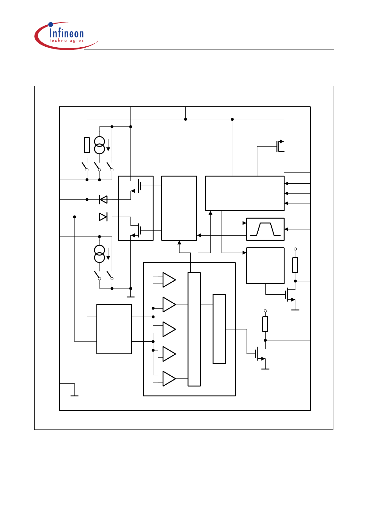
R
Functional Block Diagram
TLE 6254-3 G
RTL
CANH
CANL
RTH
9
11
12
8
V
CC
10
Output
Stage
V
S
14
Driver
Temp-
Protection
7.2
Mode Control
(normal, stand-by, sleep)
Time Out
B us F a ilu re
Wake-Up
V
Bat
Fail Flag
1
IN H
7
WK
6
ENT
5
NSTB
2
TxD
V
CC
4
NER
Filter
GND
13
Figure 2 Block Diagram
1.8
-2.8
3.2
7.2
Failure M anagement
M u ltip le x e r
Receiver
V
CC
3
AEA03314.VSD
RxD
Data Sheet 6 Rev. 2.0, 2005-03-24
TLE 6254-3 G
Circuit Description
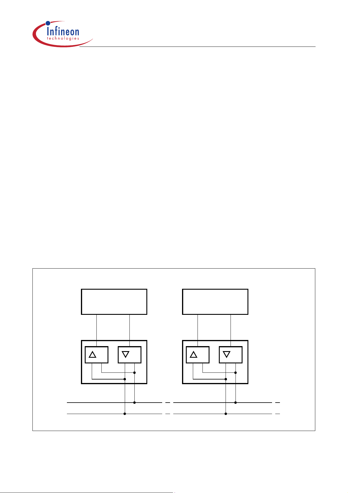
The CAN transceiver TLE 6254-3 G works as the interface between the CAN protocol
controller and the physical CAN bus-lines. Figure 3 shows the principle configuration of
a CAN network.
The TLE 6254-3 G is optimized for low-speed data transmi ssion (up to 125 kBaud) in
automotive and industrial applications.
In normal operation mode a differential sig nal is transmitted/rec eived. When bus wiring
failures are detected the device automatically switches in a dedicated single-wire mode
to maintain communication.
While no data is transferred, the power consumption c an be minimized by multiple low
power operation modes. Further a receive-only mode is implemented.
To reduce radiated electroma gnetic emission (EME) the dynam ic slopes of the CANL
and CANH signals are both limited and symmetric. This allows the use of an unshielded
twisted or parallel pair of wi res for the bus. D uring single-wi re transmission (o ne of the
bus lines is affected by a bus line failure) the EME performance of the system is
degraded from the differential mode.
In case the transmission da ta inpu t TxD is permane ntly dom inant, b oth, the CANH and
CANL transmitting stage are disabl ed after a certain delay time. This is necessary to
prevent the bus from being blocked by a defective protocol unit o r short to GND at the
TxD input.
Local Area 1
Controller 1
RxD
1
Transceiver 1
TxD
1
RxD
Transceiver 2
Local Area 2
Controller 2
2
TxD
2
Bus Line
AES02410
Figure 3 CAN Network Example
Data Sheet 7 Rev. 2.0, 2005-03-24
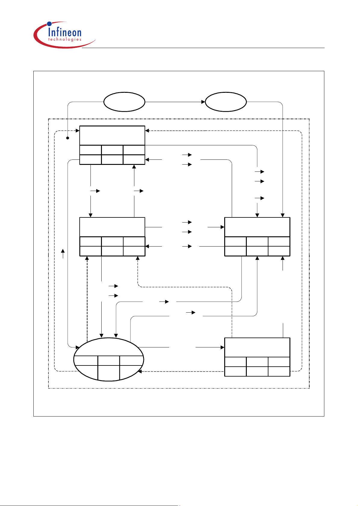
TLE 6254-3 G
Power Down
Norm al M ode
NSTB ENT IN H
1 1 High
ENT 1ENT 0
RxD-Only
NSTB ENT IN H
1 0 High
NSTB
ENT
NSTB
V
CC
NSTB 1
1
1
0 or
Low
Start Up
Power Up
NSTB
ENT
or
V
CC
V
Stand-By
Bat
NSTB ENT IN H
0 0 High
0
0
Low
NSTB 0
NSTB 0
ENT
1
Go to
Sleep M ode
NSTB ENT INH
01High
Figure 4 State Diagram
ENT
1
ENT
t
<
t
h(min)
ENT = 1
t
>
t
h(min)
W ake-U p via
CAN-Bus
or
W K-Input;
t
>
t
WU(min)
0
or
t
>
t
WK(min)
Sleep M ode
NSTB ENT IN H
0 0 Float.
AEA03317.VSD
Data Sheet 8 Rev. 2.0, 2005-03-24

TLE 6254-3 G
Operation Modes, Wake-Up
In addition to the normal operation mode, the TLE 6254-3 G offers a receive-only mode
as well as two low power operation modes to sa ve power during periods that do not
V
require communication on the CAN bus: sleep mode,
and Figure 4). Via the control input pins NSTB and ENT the operation modes are
selected by the microcontroller. In the low power modes neither receiving nor
transmitting of messages is possible.
In sleep operation mode the lowest power consumption is achieved. In order to minimize
the overall current consumption of the ECU (electronic control unit) the external voltage
regulator (5 V supply) is deactivated by th e INH output in this mode, when con nected.
For that purpose the INH output is switched to high impedance. In parallel the CANL line
is pulled-up to the battery supply voltage via the RTL output and the pull-up paths at the
input pins TxD and RxD are disabled from the internal supply.
To enter the sleep operation mode the transition mode “Go-to-Sleep” has to be selected
(Figure 4) for a minimum time
t
. After the minimum hold time t
h(min)
can be actively selected. Otherwise the TLE 6254-3 G will automatically fall in sleep
mode because of the not powered microcontroller.
stand-by mode (see Table 2
BAT
the sleep mode
h(min)
On a wake-up request either by bus line activities or via the WAKE input, the transceiver
V
is automatically set in
stand-by mode. Now the vo ltage regulator (5 V supply) is
BAT
enabled by the INH output. The WAKE input reacts to both, transitio n from high to low
voltage level as well as the other way round. To avoid faulty wake-ups due to transients
on the bus lines or the WAKE input circuitry respectively, a certain filter time is
implemented. As soon as
V
is provided, the wake-up request is monitored on both, the
CC
NERR and RxD outputs, by setting them low. Upon this the microcontroller can activate
the normal operation mode by setting the control inputs NSTB and ENT high.
The V
stand-by mode corresponds to the sleep mode, but a voltage regulator
BAT
connected to the INH output will rem ain acti ve. Wake-up req uests v ia the WAKE pin o r
the bus lines are immediatel y repo rted to the mic r oc ontrol ler by sett ing R xD and NERR
low. A power-on condition (
TLE 6254-3 G to
V
stand-by mode.
BAT
V
pin is supplied) automatically switches the
BAT
In the receive-only mode da ta on the CAN-bus are transferred t o the RxD output, but
both output stages, CAN H as well as CANL are d isabled. This means th at data at the
TxD input are not transmitted to the CAN bus . This mode is useful in comb ination to a
dedicated network-management software that allows separate diagnosis for all nodes.
A wake-up request in the receive-only mode is only reported at the RxD-output. The
NERR output in this mode is used to indicate a battery fail condition. When entering the
normal mode the
V
-flag is reset and the NERR output becomes high again. This
BAT
feature is useful e.g . when chan ging the ECU an d therefore a pre setting routine of the
microcontroller has to be started.
Data Sheet 9 Rev. 2.0, 2005-03-24

TLE 6254-3 G
If either of the supply voltages drops below the specified limits, the transceiver is
automatically switched to
Table 2 Truth Table of the CAN Transceiver
NSTB ENT Mode INH NERR RxD RTL
V
stand-by mode or power down mode respectively.
BAT
00
0 0 sleep mode
0 1 go to sleep
10Receive-only
V
stand-by
BAT
mode
1)
command
mode
V
BAT
2)
floating switched
active LOW wake-up interrupt if
V
is present
CC
switched
to V
to
becomes
floating
V
BAT
active LOW
V
power-on
BAT
3)
flag
HIGH = recessive
receive data;
LOW = dominant
switched
to
switched
to
V
V
V
BAT
BAT
BAT
CC
receive data
1 1 normal mode V
BAT
active LOW
bus error flag
HIGH = recessive
receive data;
switched
to
V
CC
LOW = dominant
receive data
1) Wake-up interrupts are rele as ed when entering normal operation mode.
2) If go to sleep command was used before, ENT may turn LOW as VCC drops, without affecting internal
functions.
3) V
power-on flag will be reseted when entering normal operation mode.
BAT
Bus Failure Management
The TLE 6254-3 G detects the bus failures as described in Table 3, and automat ically
switches to a dedicated CANH or CANL single wire mode to maintain data transmission
if necessary. Therefore, the device is equipped with one differential receiver and 4 single
ended receivers, two for each bus line. To avoid false triggering by external RF
influences the single wire modes ar e only activate d after a certain de lay time. As soon
as the bus failure disappears the transceiver switches back to differential mode after
another time delay. Bus failures are indicat ed in the normal ope ration mode by set ting
the NERR output low.
The differential receiver threshold is typ. -3.1 V. This ensu res correct reception in the
normal operation mode as well as in the failure cases 1, 2 and 4 with a noise margin as
high as possible. For these failures, further failure management is not necessary.
Detection of the failure cases 1, 2 , 3 a and 4 is only poss ible when the bu s is do min ant.
Nevertheless, they are reported on the NERR output until transmission of the next CAN
word on the bus begins.
Data Sheet 10 Rev. 2.0, 2005-03-24

TLE 6254-3 G
When one of the bus fai lures 3, 5, 6, 6a and 7 is detected, the defec tive bus wire is
disabled by switching off the affected bus termination and the respective output stage. A
wake-up from sleep mode vi a the bus is possible eithe r via a do minant CANH or CANL
line. This ensures that a wake-up is possible even if one of the failures 1 to 7 occurs.
Table 3 CAN Bus-line Failures
Failure # Failure Description
1 CANL line interrupted
2 CANH line interrupted
3 CANL line shorted to
3a CANL line shorted to V
V
BAT
CC
4 CANH line shorted to GND
5 CANL line shorted to GND
6 CANH line shorted to
6a CANH line shorted to V
V
BAT
CC
7 CANL line shorted to CANH line
A current limiting circuit protects the CAN transceiver output stages from damage by
short-circuit to positive and negative battery voltages.
The CANH and CANL pins are pro tected against el ectrical transi ents which may o ccur
in the severe conditions of automotive environments.
The transmitter output s tage s gene rate the majority of the p ow er di ss ipat ion . The refore
they are disabled if the junction temperature exceeds the maximum value. This
effectively reduces p ower dissipati on, and hence will lead to a lower chi p temperature,
while other parts of the IC can remain operating. In temperature shut-down condition the
TLE 6254-3 G is still able to receive CAN-bus messages.
Data Sheet 11 Rev. 2.0, 2005-03-24

Application Hints
Table 4 Not Needed Pins
Pin Symbol Recommendation
INH Leave open
NERR Leave open
TLE 6254-3 G
NSTB Connect to
V
ENT Connect to V
WAKE Connect to V
connect to GND: increases current consumption by approx. 5 µA
CC
CC
BAT
,
Data Sheet 12 Rev. 2.0, 2005-03-24

TLE 6254-3 G
Table 5 Absolute Maximum Ratings
Parameter Symbol Limit Values Unit Notes
Min. Max.
Input voltage at
Logic supply voltage
V
BAT
V
CC
Input voltage at TxD, RxD, NERR, NSTB
and ENT
Input voltage at CANH and CANL
Transient voltage at CANH and CANL
Input voltage at WAKE V
Input voltage at INH
Input voltage at RTH and RTL
Junction temperature
Storage temperature
Electrostatic discharge voltage at pin
CANH, CANL, RTH, RTL,
V
BAT
Electrostatic discharge voltage at any
other pin
V
S
V
CC
V
IN
V
BUS
V
BUS
WK
V
INH
V
RTH/L
T
j
T
stg
V
esd
V
esd
-0.3 40 V –
-0.3 6 V –
-0.3 VCC +
V–
0.3
-40 40 V –
-150 100 V
1)
-40 40 V –
-0.3 V
BAT
+
V–
0.3
-0.3 40 V –
-40 160 °C–
-55 155 °C–
-4 4 kV
-2 2 kV
2)
2)
1) See ISO 7637
2) Human body model: equivalent to discharging a 100 pF capac it or th rough a 1.5 kΩ resistor.
Note: St resses above those listed here may cause permanent damage to the devi ce.
Exposure to absolute maximum rating conditions for extended periods may affect
device reliability.
Data Sheet 13 Rev. 2.0, 2005-03-24

TLE 6254-3 G
Table 6 Operating Range
Parameter Symbol Limit Values Unit Notes
Min. Max.
Logic input voltage
Battery input voltage
Termination resistances at RTL and
V
CC
V
S
R
RTL/H
4.75 5.25 V –
5.7 27 V –
0.5 16 kΩ –
RTH
Junction temperature
T
j
-40 150 °C–
Thermal Resistance
Junction ambient
R
thja
– 120 K/W –
Thermal Shutdown
Junction temperature
T
jSH
160 200 °C10 °C
hyst.
Wake Input Voltage
Wake input voltage
V
WK
-0.3 27 V –
Note: In the operating range, the functions given in the circuit description are fulfilled.
Data Sheet 14 Rev. 2.0, 2005-03-24

Table 7 Static Characteristics
TLE 6254-3 G
4.75 V ≤
V
≤ 5.25 V; 6 V ≤ VS ≤ 27 V; normal operation mode; -40 ≤ Tj ≤ +125 °C (unless
CC
otherwise specified). All vol tages are defined with respect to ground. Positive current
flowing into the IC.
Parameter Symbol Limit Values Unit Notes
Min. Typ. Max.
Supplies
Supply current I
V
CC
, V
S
CC
– 3.5 10.0 mA recessive;
TxD =
V
CC
– 6.5 10 mA dominant;
TxD = 0 V; no load
Supply current
I
CC
– 3.5 10.0 mA –
(Receive-only mode)
Supply current
V
stand-by)
(
BAT
Supply current
(
V
stand-by)
BAT
I
CC
I
S
I
CC + IS
–2555µA VCC = 5 V;
V
= 12 V
–3050µA
S
55 85 µA VCC = 5 V;
V
= 12 V
S
T
= 25 °C
j
Supply current
I
S
–5070µA VCC = 0 V;
(sleep op eration mo de)
Supply current
I
S
–5065µA VCC = 0 V;
(sleep op eration mo de)
Battery voltage for
V
S
-13.5V
setting power-on flag
Receiver Output RxD and Error Detection Output NERR
HIGH level output
voltage (pin NERR)
HIGH level output
voltage (pin RxD)
LOW level output voltage
V
V
V
OH
OH
OL
V
-
CC
– V
CC
0.9
V
-
CC
– V
CC
0.9
0–0.9VI0 = 1.25 mA
V
= 12 V
S
V
= 12 V
S
T
= 25 °C
j
V I0 = -100 µA
V I0 = -250 µA
Data Sheet 15 Rev. 2.0, 2005-03-24

TLE 6254-3 G
Table 7 Static Characteristics (cont’d)
V
4.75 V ≤
otherwise specified). All vol tages are defined with respect to ground. Positive current
flowing into the IC.
Parameter Symbol Limit Values Unit Notes
Transmission Input TxD, not Stand-By NSTB and Enable Transfer ENT
≤ 5.25 V; 6 V ≤ VS ≤ 27 V; normal operation mode; -40 ≤ Tj ≤ +125 °C (unless
CC
Min. Typ. Max.
HIGH level input voltage
LOW level input voltage
HIGH level input current
(pins NSTB and ENT)
LOW level input current
(pins NSTB and ENT)
HIGH level input current
(pin TxD)
LOW level input current
(pin TxD)
Forced battery voltage
stand-by mode (fail safe)
Wake-up Input WAKE
Input current
V
V
I
I
I
I
V
I
IH
IL
IH
IL
IL
IH
IL
CC
0.7 ×
V
CC
-0.3 – 0.3 ×
– VCC +
0.3
V
CC
V–
V–
–2080µA Vi = 4 V
0.7 6 – µA Vi = 1 V
-150 -30 -5 µA Vi = 4 V
-600 -300 -40 µA Vi = 1 V
2.75 – 4.5 V –
-3 -2 -1 µA VWK = 0 V
Wake-up threshold
V
WK(min)
2.2 3.0 3.9 V V
NSTB
= 0 V
voltage
Inhibit Output INH
HIGH level voltage drop
∆
V
= VS - V
H
INH
Leakage current
∆V
I
INH,lk
H
–0.10.8VI
= -0.18 mA
INH
-5.0 – 5.0 µA sleep operation
mode;
V
= 0 V
INH
Data Sheet 16 Rev. 2.0, 2005-03-24

Table 7 Static Characteristics (cont’d)
TLE 6254-3 G
4.75 V ≤
V
≤ 5.25 V; 6 V ≤ VS ≤ 27 V; normal operation mode; -40 ≤ Tj ≤ +125 °C (unless
CC
otherwise specified). All vol tages are defined with respect to ground. Positive current
flowing into the IC.
Parameter Symbol Limit Values Unit Notes
Min. Typ. Max.
Bus Lines CANL, CANH
Differential receiver
V
dRxD(rd)
-3.6 -3.1 -2.6 V VCC = 5.0 V
recessive-to-dominant
threshold voltage
Differential receiver
V
dRxD(dr)
-3.6 -3.1 -2.6 V VCC = 5.0 V
dominant-to-recessive
threshold voltage
CANH recessive output
voltage
CANL recessive output
voltage
CANH dominant output
voltage
V
CANH,r
V
CANL,r
V
CANH,d
0.10 0.15 0.30 V TxD = VCC;
R
< 4 kΩ
RTH
V
-
CC
0.2
V
CC
1.4
––VTxD = VCC;
R
-
V
-
CC
1.0
V
CC
VTxD = 0 V;
V
R
< 4 kΩ
RTL
= 5V;
CC
= 100Ω
L
CANL dominant output
voltage
CANH output current
CANL output current
V
CANL,d
I
CANH
I
CANL
– 1.0 1.4 V TxD = 0 V;
V
= 5V;
CC
R
= 100Ω
L
-110 -80 -50 mA V
CANH
= 0 V;
TxD = 0 V
-5 0 5 µA sleep operation
mode;
V
50 80 110 mA V
CANH
CANL
= 12 V
= 5 V;
TxD = 0 V
-5 0 5 µA sleep operation
mode;
V
V
= 0 V;
CANL
= 12 V
S
Data Sheet 17 Rev. 2.0, 2005-03-24

TLE 6254-3 G
Table 7 Static Characteristics (cont’d)
V
4.75 V ≤
otherwise specified). All vol tages are defined with respect to ground. Positive current
flowing into the IC.
Parameter Symbol Limit Values Unit Notes
≤ 5.25 V; 6 V ≤ VS ≤ 27 V; normal operation mode; -40 ≤ Tj ≤ +125 °C (unless
CC
Min. Typ. Max.
Voltage detection
threshold for short-circuit
to battery voltage on
CANH and CANL
CANH wake-up voltage
threshold
CANL wake-up voltag e
threshold
CANH single-ended
receiver threshold
CANL single-ended
receiver threshold
Difference of wake-up
threshold
CANL leakage current
V
det(th)
V
CANH,wu
V
CANL,wu
V
CANH
V
CANL
V
diff,wu
I
CANL,lk
6.5 7.3 8.0 V –
1.1 2.2 2.5 V –
2.5 3.1 3.9 V –
1.5 1.8 2.3 V failure cases 3, 5
and 7;
V
= 5 V
CC
2.8 3.1 3.5 V failure case 6 and
V
6a;
= 5 V
CC
0.8 V
-5 0 5 µA VCC = 0 V; VS = 0 V;
V
T
= 12 V;
CANL
< 85 °C
j
CANH leakage current
Data Sheet 18 Rev. 2.0, 2005-03-24
I
CANH,lk
-5 0 5 µA VCC = 0 V; VS = 0 V;
V
T
= 5 V;
CANH
< 85 °C
j

Table 7 Static Characteristics (cont’d)
TLE 6254-3 G
4.75 V ≤
V
≤ 5.25 V; 6 V ≤ VS ≤ 27 V; normal operation mode; -40 ≤ Tj ≤ +125 °C (unless
CC
otherwise specified). All vol tages are defined with respect to ground. Positive current
flowing into the IC.
Parameter Symbol Limit Values Unit Notes
Min. Typ. Max.
Termination Outputs RTL, RTH
RTL to
V
switch-on
CC
R
RTL
–2095Ω Io = -10 mA
resistance
RTL to BAT switch series
resistance
R
oRTL
81530kΩ V
stand-by or
BAT
sleep operation
mode
RTH to ground switch-on
R
RTH
–4095Ω Io = 10 mA
resistance
RTH output voltage
V
oRTH
–0.71.0VIo = 1 mA;
low power mode
RTH pull-down current
I
RTH,pd
40 75 120 µA failure cases 6 and
6a
RTL pull-up current
RTH leakage current
RTL leakage current
I
RTL,pu
I
RTH,lk
I
RTL,lk
-120 -75 -40 µA failure cases 3, 5
and 7
-5 0 5 µA VCC = 0 V;
V
= 0 V;
S
V
= 5 V;
RTH
T
< 85 °C
j
-10 0 10 µA VCC = 0 V;
V
= 0 V;
S
V
= 12 V;
RTL
T
< 85 °C
j
Data Sheet 19 Rev. 2.0, 2005-03-24

Table 8 Dynamic Characteristics
TLE 6254-3 G
4.75 V ≤
V
≤ 5.25 V; 6 V ≤ VS ≤ 27 V; normal operation mode; -40 ≤ Tj ≤ +125 °C (unless
CC
otherwise specified). All vol tages are defined with respect to ground. Positive current
flowing into the IC.
Parameter Symbol Limit Values Unit Notes
Min. Typ. Max.
CANH and CANL bus
output transition time
recessive-to-dominant
CANH and CANL bus
output transition time
dominant-to-recessive
Minimum dominant time
for wake-up via CANL or
t
rd
t
dr
t
wu(min)
0.6 1.2 2.4 µs 10% to 90%;
C
= 10 nF;
1
C
= 0; R1 = 100 Ω
2
0.3 0.6 1.3 µs 10% to 90%;
C
= 1 nF; C2 = 0;
1
R
= 100 Ω
1
82540µs stand-by modes;
V
= 12 V
S
CANH
Minimum wake-up time on
pin WAKE
Failure cases 3, 6
t
WK(min)
t
fail
82550µs Low power modes;
V
= 12 V
S
20 40 80 µs Normal Mode
detection time
Failure case 6a
detection time
Failure cases 5, 7
detection time
Failure cases 5, 6, 6a, 7
recovery time
Failure cases 3
recovery time
Failure cases 5, 7
detection time
Failure cases 5, 7
recovery time
Failure cases 6, 6a
detection time
Failure cases 6, 6a
recovery time
248msNormal Mode
1.0 2.0 4.0 ms Normal Mode
20 40 80 µs Normal Mode
250 500 750 µs Normal Mode
0.4 1.0 2.4 ms stand-by modes;
V
= 12 V
S
0.4 1.0 2.4 ms stand-by modes;
V
= 12 V
S
0.8 4.0 8.0 ms stand-by modes;
V
= 12 V
S
0.4 1.0 2.4 ms stand-by modes;
V
= 12 V
S
Data Sheet 20 Rev. 2.0, 2005-03-24

Table 8 Dynamic Characteristics (cont’d)
TLE 6254-3 G
4.75 V ≤
V
≤ 5.25 V; 6 V ≤ VS ≤ 27 V; normal operation mode; -40 ≤ Tj ≤ +125 °C (unless
CC
otherwise specified). All vol tages are defined with respect to ground. Positive current
flowing into the IC.
Parameter Symbol Limit Values Unit Notes
Min. Typ. Max.
Propagation delay
TxD-to-RxD LOW
(recessive to dominant)
t
PD(L)
–1.32.4µs C1 = 100 pF;
C
= 0; R1 = 100 Ω;
2
no failures and bus
failure cases 1, 2,
3a, 4
–1.52.4µs
C
= C2 = 3.3 nF;
1
R
= 100 Ω; no bus
1
failure and failure
cases 1, 2, 3a, 4
–1.62.5µs
C
= 100 pF; C2 = 0;
1
R
= 100 Ω; bus
1
failure cases 3, 5,
6, 6a
Propagation delay
TxD-to-RxD HIGH
(dominant to recessive)
t
PD(H)
–1.82.6µs
C
= C2 = 3.3 nF;
1
R
=100 Ω; bus
1
failure cases 3, 5,
6, 6a
–1.22.4µs C1 = 100 pF;
C
= 0; R1 =100 Ω;
2
no failures and bus
failure cases 1, 2,
3a, 4
–2.53.5µs
C
= C2 = 3.3 nF;
1
R
= 100 Ω; no bus
1
failure and failure
cases 1, 2, 3a, 4
Data Sheet 21 Rev. 2.0, 2005-03-24

Table 8 Dynamic Characteristics (cont’d)
TLE 6254-3 G
4.75 V ≤
V
≤ 5.25 V; 6 V ≤ VS ≤ 27 V; normal operation mode; -40 ≤ Tj ≤ +125 °C (unless
CC
otherwise specified). All vol tages are defined with respect to ground. Positive current
flowing into the IC.
Parameter Symbol Limit Values Unit Notes
Min. Typ. Max.
Propagation delay
TxD-to-RxD HIGH
(dominant to recessive)
t
PD(H)
–1.02.1µs C1 = 100 pF; C2 = 0;
R
= 100 Ω; bus
1
failure cases 3, 5,
6, 6a
–1.52.6µs
C
= C2 = 3.3 nF;
1
R
= 100 Ω; bus
1
failure cases 3, 5,
6, 6a
Minimum hold time to go
t
h(min)
15 30 60 µs–
sleep command
Edge-count difference
(falling edge) between
n
e
–4––normal operating
mode
CANH and CANL for
failure cases 1, 2, 3a, 4
detection NERR becomes
LOW
Edge-count difference
(rising edge) between
CANH and CANL for
failure cases 1, 2, 3a, 4
recovery
TxD permanent dominant
disable time
t
TxD
–2––normal operating
mode
1.32.03.5ms–
Data Sheet 22 Rev. 2.0, 2005-03-24

Test and Application
+ 5 V
73654 21
RxDNERR TxDENTWAKE NSTB INH
TLE 6254-3G
CAN Transceiver
RTH RTL CANH CANL GND
V
CC
V
BAT
141312111098
R
1
R
1
TLE 6254-3 G
20 pF
+ 12 V
CC
2
CAN Bus Substitute 1
R
1
C
K
C
11
R
= 100 Ω
1
C
= 10 nF
1,2
= 1 nF
C
R
1
C
K
K
Schaffner
Generator
CAN Bus Substitute 2
AES02423
Figure 5 Test Circuits
For isolated testing the CAN Bus Substitute 1 is connected to the CAN Transceiver (see
Figure 5). The capacitors
termination resistors
R
RTH
C
1-2
and R
simulate the cable. Allowed minimum values of the
are 500 Ω. Electromagnetic interference on the bus
RTL
lines is simulated by switching to CAN Bus Substitute 2. The waves of the applied
transients will be in accordance with ISO 7637 part 1, test 1, test pulses 1, 2, 3a and 3b.
Data Sheet 23 Rev. 2.0, 2005-03-24

TLE 6254-3 G
V
Bat
CAN
Bus
1)
100
nF
Choke
R
RTH
R
RTL
10 k
Ω
TLE 6254-3G
11
CANH
12
CANL
8
RTH
9
RTL
14
V
S
7
WK
1
IN H
NERR
GND
RxD
TxD
ENT
NSTB
V
CC
3
2
6
5
4
10
100
nF
µP
w ith O n -C h ip
CAN -module
e.g.
C50C, C 164C
GND
IN H
V
+
22 µF 100 nF
1) O ptional, according to car m anufacturers requirements
Figure 6 Application Example
E.g.
TLE 4263
TLE 4299
TLE 4271
TLE 4276
S
GND
V
CC
+
22 µF
AEA03307.VSD
Data Sheet 24 Rev. 2.0, 2005-03-24

Package Outlines
-0.15
0.25
(1.47)
1.75 MAX.
+0.05 1)
4
-0.13
0.33 x 45˚
A
+0.05
-0.01
0.2
TLE 6254-3 G
MAX.
8˚
0.41
1.27
+0.08
-0.06
0.1
M
0.2548B
C
C
14x
±0.2
6
14
+0.05
-0.11
7
1)
B
1
8.69
Index Marking
1)
Does not include plastic or metal protrusion of 0.25 max. per side
Figure 7 P-DSO-14-19 (Plastic Dual Small Outline)
0.64
+0.25
-0.23
14x
0.254
M
A
GPS09330
You can find all of our packages, sorts of packing and others in our
Infineon Internet Page “Products”: http://www.infineon.com/products.
SMD = Surface Mounted Device
Dimensions in mm
Data Sheet 25 Rev. 2.0, 2005-03-24
 Loading...