

现货库存、技术资料、百科信息、热点资讯,精彩尽在鼎好!
Final Data Sheet, Rev. 3.2, Apr. 2006
TLE 6251 G
High Speed CAN-Transceiver with Wake
Detection
Automotive Power
Never stop thinking.

Edition 2006-04-05
Published by Infineon Technologies AG,
St.-Martin-Strasse 53,
81669 München, Germany
© Infineon Technologies AG 2005.
All Rights Reserved.
Attention please!
The information herein is given to de scribe certai n compon ents a nd shall not be consi dered as a guarantee of chara cte risti cs.
Terms of delivery and ri ghts to techni c al change rese r v e d .
We hereby disclaim any and all warranties, including but not limited to warranties of non-in fringement, regarding circuits,
descriptions and charts stated herein.
Information
For further information on tec hnology, delivery terms and conditions and prices please contact your ne arest Infineon
Technologies Office (www.infineon.com).
Warnings
Due to technical requirements components may contain danger ous substances. For information on the types in question
please contact your nearest Infineon Technologies Office.
Infineon T echn ologies Compone nts may only be used in life- support devices or systems with the expr ess written appr oval of
Infineon Technologies, if a failure of such components can reasonably be expected to cause the failure of that life-support
device or system, or to af fect the safe ty or effecti veness of that dev ice or system. Life su pport devices or syst ems are intended
to be implanted in the human body, or to support and/or maintain and sustain and/or protect human life. If they fail, it is
reasonable to assume that the health of the user or other persons may be endangered.
High Speed CAN-Transceiver with Wake Detection
3
Features
• CAN data transmission rate up to 1 Mbaud
• Compatible to ISO/DIS 11898
• Supports 12 V and 24 V automotive applications
• Low power modes with local wake-up input and
remote wake-up via CAN bus
• Very low power consumption in sleep mode
• Wake-up input
• Wake-up source recognition
• Inhibit output to control an external power supply
• Diagnosis output
• RxD only mode for node failure analysis
• Split termination to stabilize the recessive level
• TxD time-out function with diagnosis
• RxD recessive clamping handler with diagnosis
• TxD to RxD short circuit handler with diagnosis
• Bus line short circuit diagnosis
• Bus dominant clamping diagnosis
• Undervoltage detection at
• Cold start diagnosis (first battery connection)
• Adaptive to host logic supply levels (3.3 and 5 V)
• Wide common mode range for electromagnetic immunity (EMI)
• Low electromagnetic emission (EME)
• Short circuit proof to ground, battery and
• Overtemperature protection
• Protected against automotive trans ien ts
• +/- 6kV ESD Robustness according to IEC 61000-4-2
V
CC
, V
and V
I/O
V
BAT
CC
TLE 6251 G
P-DSO-14-1
Type Ordering Code Package
TLE 6251 G SP000069400 P-DSO-14-13
Final Data Sheet 3 Rev. 3.2, 2006-04-05

TLE 6251 G
Description
The CAN-transceiver TLE 6251 G is a mono lithic integrate d circ uit in a P-DSO-14-13 packa ge
for high speed differential mode data transmission (up to 1 Mbaud) and re ce ptio n in automotive
and industrial applications. It works as an interface between the CAN protocol controller and the
physical bus lines compatible to ISO/DIS 11898.
As a successor to the first generation of H S CAN, the TLE 6251 G is designe d to provide an
excellent passive behavior when the transceiver is switched off (mixed networks, clamp15/30
applications). The current consumption can be reduced, due to the low power modes.. This
supports networks with partially powered down nodes.
The TLE 6251 G offers two low powe r modes as well as a receive-only mode to support software
diagnosis functions. A wake-up from the low power mode is possible via a message on the bus or
via the bi-level sensitive wake input. An external voltage supply IC can be controlled by the
inhibit output. So, the µC can be po wered down and the TLE 6251 G stil l reacts to wake-up
activities on the CAN bus or local wake input.
A diagnosis output allows mode dependent enhanced diagnosis of bus failures and wake-up
source. A
V
fail flag reports an power-on condition at the battery supply input.
BAT
The TLE 6251 G is designed to withstand the severe condit ions of automotive applications and
to support 12 V and 24 V applications.
The IC is based on the Smart Power Technology SPT
®
which allows bipolar and CMO S co ntr ol
circuitry in accordance with DMOS power devices existing on the same monolithic circuit.
Final Data Sheet 4 Rev. 3.2, 2006-04-05
Pin Configuration
TLE 6251 G
TLE 6251 G
(P-D S O-14-1 3 )
1TxD
GND
V
CC
RxD
V
µC
EN
INH
2
3
4
5
6
7
AEP03398.VSD
Figure 1 Pin Configuration (top view)
Table 1 Pin Definitions and Functions
14
13
12
11
10
NSTB
CANH
CANL
SPLIT
V
S
9
8
WK
NERR
Pin No. Symbol Function
1TxDCAN transmit data input; 20 kΩ pull-up, LOW in dominant state
2 GND Ground
3
V
CC
5 V supply input; block to GND with 100 nF ceramic capacitor
4RxDCAN receive data output; LOW in dominant stat e, pus h -pull output
stage
5
V
µC
Logic voltage level adapter input; connect to pin VCC for 5 V
microcontroller, connect to additional supply voltage for other logic
voltage levels, block to GND with 100 nF ceramic capacitor
6ENMode control input 1; internal pull-down, see Figure 6
7INHControl output; set HIGH to activate voltage regulator; open drain
8NERRDiagnosis outp ut 1; error and power on indication output, push-pull
output stage
9WKWake-up input; bi-level sensitive
Final Data Sheet 5 Rev. 3.2, 2006-04-05
Table 1 Pin Definitions and Functions (cont’d)
Pin No. Symbol Function
TLE 6251 G
10 V
S
Battery voltage supply input; block to GND with 100 nF ceramic
capacitor
11 SPLIT Termination output; to support the recessive voltage level of the bus
lines (see Table 2)
12 CANL Low line output; LOW in dominant state
13 CANH High line output; HIGH in dominant state
14 NSTB Mode control input 2; in ternal pull-down, see Figure 6
Final Data Sheet 6 Rev. 3.2, 2006-04-05
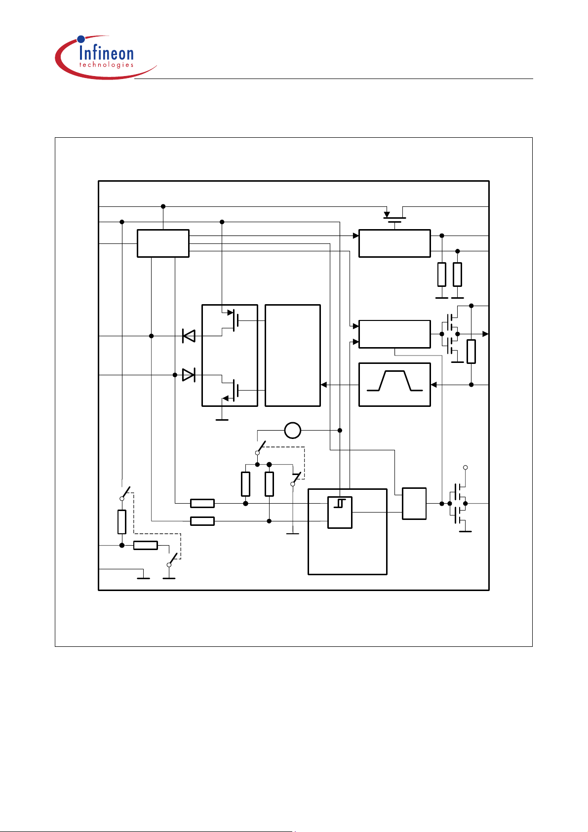
Functional Block Diag ram
TLE 6251 G
V
V
CC
WK
CANH
CANL
10
S
3
9
Wake-Up
Logic
13
TLE 6251 G
Driver
Mode Control
Logic
Diagnosis
Logic
14
7
6
5
8
INH
EN
NSTB
V
µC
NERR
Output
12
Stage
Temp.-
Protection
1
+
TxD
timeout
=
V
µC
GND
11
2
SPLIT
Figure 2 Block Diagram
Receiver
+
Bus Failure
Detection
MUX
4
AEB03397.VSD
RxD
Final Data Sheet 7 Rev. 3.2, 2006-04-05

TLE 6251 G
Application Information
As a successor to the first generation of H S CAN, the TLE 6251 G is designe d to provide an
excellent passive behavior when the transceiver is switched off (mixed networks, terminal 15/30
applications). The current consumption can be reduced, due to the low power modes. This
supports networks with partially powered down nodes.
A wake-up from the low power modes is possible via a message on the bus or via the bi-level
sensitive wake input WK. An extern al vo ltage sup ply IC ca n be controlle d by the in hibit output
INH. So, the µC can be powered down and the T LE 6251 G still reacts to wake-up activities on
the CAN bus or local wake input activities.
A diagnosis o utput pin NERR, allows mode dependent en hanced diagnosis of bus failures and
wake-up source. A
V
fail flag will be resetted after the first transition into normal mode.
BAT
The TLE 6251 G has four opera tion modes, the normal, the receive onl y, the stand by mode and
the sleep mo de. These modes can be controlled with the two contro l pins EN and NSTB pin (s ee
Figure 6, Table 2). Both, EN and NSTB, have an implemented pull-down, so if there is no signal
applied to EN and NSTB, the transceiver automatically changes to the standby mode.
V
fail flag reports a power-on con dition at the battery supp ly input. The
BAT
Normal Mode
To transfer the TLE 6251 G into the normal mo de, NSTB an d EN have to be switc hed to HI GH
level. This mode is designed for the normal data transmission/reception within the HS-CAN
network.
Transmission
The signal from the µC is applied to the TxD input of the TLE 6251 G. Now the bus driver
switches the CANH/L output stages to transfer this input signal to the CAN bus lines.
TxD Time-out Feature
If the TxD signal is dominant for a time
t > t
, the TxD time-out function deactivates the
TxD
transmission of the signal at the bus. This is realized to prevent the bus from being blocked
permanently due t o an error.
The transmis sion is released again, after a mode state change.
TxD to RxD Short Circuit Feature
Similar to the TxD time-out, a TxD to RxD short circuit would also drive a permanent dominant
signal at the bus and so block the communication. To avoid this, the TLE 6251 G has a TxD to
RxD short circuit detection.
Final Data Sheet 8 Rev. 3.2, 2006-04-05
TLE 6251 G
Reduced Electromagnetic Emission
The bus driver has an imple mented control to reduce the electromagnetic emission (EME). This
is achieved by controlling the symmetry of the slope, resp. of CANH and CANL.
Overtemperature
The driver st ages are protected against overtemperatu re. Exceeding the s hutdown temperature
results in deactivation of the driving stages at CANH/L. To avoid a bit failure after cooling down,
the signals can be transmitted again only after a dominant to recessive edge at TxD.
Figure 3 shows the way how the transmission stage is deactivated and activated again. First an
overtemperatu re condit ion causes the transmissi on stage to de activate . After the ov ertemperat ure
condition is no longer present, the transmission is only possible afte r the TxD bus signal has
changed to recessive level.
Failure
Overtemp
V
GND
TxD
V
GND
CANH
V
V
CC
CC
Overtemperature
t
CC
t
CC
DRR
/2
t
AET03394.VSD
Figure 3 Release of the Transmission after Overtemperature
Final Data Sheet 9 Rev. 3.2, 2006-04-05

TLE 6251 G
Reception
The analog CAN bus signals are c onver ted in to a d igital signal at RxD vi a t he differen tial in put
receiver.
In normal mode and RxD only, the split pin is used to stabilize the recessive common mode
signal.
Permanent Rece ssive Clamping
If the RxD signal is permanent recessive, although there is a message sent on the bus, the host µC
of this transceiver could start a message at any time, because the bus seems to be idle. To pr event
this node to disturb the communication on the bus, the TLE 6251 G offers a so called permanent
RxD recessive clamping. If the RxD signal is perm anent recessive , an error fla g is set and the
transmitter is deactivated as long as the error occurs
Receive Only Mode (RxOnly Mode)
In the RxOnly mode, the transmission stage is deactiva ted but the reception of signals via the
CAN bus is still possible. This mode is implemented to support hardware and software diagnosis
functions.
If there is an hardware error on the transmiss ion pa rt of a node (e.g. bubbling idiot failure), in the
RxOnly mode, the bu s is no l ong er b loc ke d and t he µC c an st ill re ce ive the m ess ages o n th e b us.
It is also possible to make a network analysis of the interconnections between the nodes. A
connection bet ween two nod es (in a network) is checked if both nodes a re in the normal mode
and all others are in RxOnly mode. If a message from one node is sent to the other, this has to be
acknowledged. If there is no acknowledge of the message, the connection between the two nodes
has an error.
The RxD pin also works as an diagnosis flag, which is described more in detail in Table 2.
Final Data Sheet 10 Rev. 3.2, 2006-04-05

TLE 6251 G
Standby Mode
In the standby mode, transmission and reception of signals is deactivated. This is the first step of
reducing the current consumption. The internal voltage regulator control pin (INH) is still active,
so all external (INH controlled) powered devices are also activated.
Wake-Up
The wake-up is possible via WK-pin (filtering ti me
t
) and sets the RxD/NER R pins to L OW, see Figure 4. Now the µC is able to detect this change
WU
t > t
) or CAN message (fil terin g time t >
WK
at RxD and switch the transceiver int o the normal mode. Once the wake-up flag is set (= LOW),
it remains in this state, as long as the transceiver is not transferred into the normal mode. The
detection of the wake-up source is possible during the first 4 recessive to dominant edges at TxD
in the normal mode.
Go-to Sleep Mode
The go-to sleep mode is used to have an inte rmediate step betwee n the slee p mode and all o ther
modes. This mod e has to contr ol if the sleep command (EN = 1, NSTB = 0) i s activated for a
minimum hold time
t > t
. Afterwards the TLE 6251 G automatically tran sfers into the sleep
hSLP
mode. The activated features in go-to sleep mode are similar to the standby mode.
Sleep Mode
In the sleep mode, transmission and reception of signals is deactivated. This is the second step of
reducing the current consumption. The internal voltage regulator control pin (INH) is deactivated.
Transition into other Modes during Sleep Mode
V
Transition from sleep into other modes is possible if
and VµC active. Selection of the modes
CC
can be done by the mode control inputs.
Wake-Up
The wake-up is possible via WK-pin (filtering ti me
t
) and automatically transfers the TLE 6251 G into the standby mode and sets the RxD/NERR
WU
t > t
) or CAN message (fil terin g time t >
WK
pins to LOW, see Figure 4. Onc e th e TLE 6251 G has been set to the standby m od e, th e s y ste m
voltage regulator is acti vated by the inhibit o utp ut INH, and th e µC restarts. Now the µC is able
to detect this change at RxD and switch the transceiver into the normal mode. Once the wake-up
flag is set (= LOW), it remains in this state, as long as th e transceiver is not transferre d into the
normal mode. The detection of the wake-up source is possible during the first 4 recessive to
dominant edges at TxD in the normal mode.
Final Data Sheet 11 Rev. 3.2, 2006-04-05

TLE 6251 G
CAN_H
CAN_L
BUS
OFF
Vdiff
INH
Vcc/Vio
BUS
WAIT
WAKE
PATTERN
t
WU
DEVICE
WAKE
ECU WAKE
LDO RAMP UP
Communication
starts
µC P.O.R.
RxD
NERR
NSTB/EN
µC set TLE6251G to
Figure 4 RxD during Sleep mode
normal operation
Normal mode
Final Data Sheet 12 Rev. 3.2, 2006-04-05

TLE 6251 G
Split Circuit
The split circuitry is activated during normal and RxOnly mode and deactivated (SPLIT pin high
ohmic) during sleep and standby mode. The SPLIT pin is used to stabilize the recessive common
mode signal in normal mo de and RxOnly mode . This is realiz ed with a stabiliz ed vol tage of 0.5
V
at SPLIT.
CC
CANH
TLE 6251 G/DS
SPLIT
CANL
10
nF
60 Ω
Split
Termination
60 Ω
Split
Termination
at Stub
CAN
Bus
10
nF
1.5 kΩ1.5 kΩ
SPLIT
TLE 6251 G/DS
60 Ω
Split
Termination
60 Ω
CANLCANH
CANH
TLE 6251 G/DS
SPLIT
10
nF
CANL
AEA03399.VSD
Figure 5 Application example for the SPLIT Pin
A correct application of the SPLIT pin is shown in Figure 5. The split termination for the left and
right node is realized with two 60 Ω resistances and one 10 nF cap acito r. The cent er no de in this
example is a stub node and the recommended value for the split resistances is 1.5 kΩ.
Diagnosis-Flags at NERR and RxD
Power-Up Flag
• Task: to signalize a power-up state at
Final Data Sheet 13 Rev. 3.2, 2006-04-05
V
BAT

• Indicator: NERR = LOW in RxOnly mode
• Remarks: Power-up flag is cleared when entering the normal mode
Wake-Up Flag
TLE 6251 G
• Task: to signalize a wake-up condition at the WK pin (filtering time
message (filtering time
t > t
WU
)
t > t
) or via CAN bus
WK
• Indicator: RxD or NERR = LOW in sleep/stand-by mode immediately after wake-up
• Remarks: Flag is cleared on entering the RxOnly mode
Wake-Up Source Flag
• Task: to distinguish between the two wake-up sources
• Indicator: NER R = LOW in normal mode = wake-up via WK pi n
• Remarks: only available if the po wer-up flag is cleared. After four recessive to dominant
edges on TxD in no rmal mode, the flag is cle ared. Leav ing t he norma l mode cle ars the wakeup source flag.
Bus Failure Flag
V
• Task: to signalize a bus line short circuit condition to GND,
or V
S
CC
• Indicator: NERR = LOW in normal mode
• Remarks: flag is set after four consecutive recessiv e to dominant cycles on pin TxD when
trying to drive the bus dominant. The bus failure flag is cleared if the normal mode is
reentered or 4 recessive to dominant edges at TxD without failure condition.
Local Failure Flag
• Task: to signalize one of the five loc al failure condition s described in Local Failure -Flags
and -Detection
• Indicator: NERR = LOW in RxOnly mode (local failure flag is set)
• Remarks: the f lag is cleared when entering the normal mode from RxOnly mo de or when RxD
is dominant while TxD is recessive.
Final Data Sheet 14 Rev. 3.2, 2006-04-05

Local Failure-Flags and -Detection
TxD Dominant Failure Detection
TLE 6251 G
• Effect: permanent dominant signal for
t > t
TxD
at TxD
• Indicator: NERR = LOW in RxOnly mode (local failure flag is set)
• Action: disabling of the transmitter stage
• Remarks: release of the transmitter stage only after transition into RxOnly mode (failure
diagnosis) and transition into normal mode.
RxD Permanent Recessive Clamping
• Effect: inte rnal Rx D sign al do es not m atch sign al a t RxD pi n be cause the RxD p in is pull ed
to HIGH (permanent HIGH)
• Indicator: NERR = LOW in RxOnly mode (local failure flag is set)
• Action: disabling of the receiver stage
• Remarks: the flag is cleared by changing from RxOnly (failure diagnosis) into normal mode
or RxD gets dominant.
TxD to RxD Short Cir cu i t
• Effect: short circuit between RxD and TxD
• Indicator: NERR = LOW in RxOnly mode (local failure flag is set)
• Action: disabling of the transmitter stage
• Remarks: the flag is cleared by cha nging from Rx Only (failu re di agno sis) into no rmal mode .
Bus Dominant C lamping
• Effect: permanent dominant signal at the CAN bus for
t > t
BUS
• Indicator: NERR = LOW in RxOnly mode (local failure flag is set)
• Action: none
• Remarks: none
Overtemperature Detection
• Effect: junction temperature at the driving stages exceeded
• Indicator: NERR = LOW in RxOnly mode (local failure flag is set)
• Action: disabling of the transmitter stage
• Remarks: the flag is cleared by changing from RxOnly (failure diagnosis) into normal mode
or RxD gets dominant. Bus only released after the next dominant bit in TxD.
Final Data Sheet 15 Rev. 3.2, 2006-04-05

TLE 6251 G
Other Features
V
-level Adapter
µC
The advantage of the adaptive µC logic is the ratiometrical scaling of the I/O levels depending on
V
the input voltage at t he
internal logic levels of the TLE 6251 G.
WAKE Input
The wake-up input pin is a bi -level sensitive input. This means that both tran sitions, HIGH to
LOW and LOW to HIGH, result in a wake-up.
V
, VµC Undervoltage Detection
CC
If an undervoltage c ondition at
automatically transfers into the sleep mode and the undervoltage flag is set. This flag is an internal
flag and not available via NERR or RxD. The flag is cl ea red agai n , afte r setting the po wer on or
wake flag (power-up or wake-up).
pin. So it can be ensured that the I/O voltage of the µC fits to the
µC
V
, VµC is detected for longer than t = t
CC
, the TLE 6251 G
UV,t
V
Undervoltage Detection
S
V
If an undervolt age condition at
is detected, the TLE 6251 G immediately transfers into the
S
standby mode and the u ndervolta ge flag is set. Th is flag is an in ternal flag a nd not avail abl e via
NERR or RxD. The flag is cleared ag ain, after the supply voltage
V
has reached the nominal
S
value.
Final Data Sheet 16 Rev. 3.2, 2006-04-05

TLE 6251 G
Normal Mode
EN NSTB IHH
1 1 High
Go to Sleep
NSTBEN
Power Down
Start Up
Power Up
Undervoltage
at
V
S
Receive-Only
EN NSTB INH
01
0 1 High
Stand-By
EN NSTB INH
0 0 High
t < t
hSLP
t > t
hSLP
Figure 6 Mode State Diagra m
Undervoltage
V
at
CC /VµC
for t > t
UV,t
Wake-Up:
t > t
WK
t > t
WU
Sleep
EN NSTB IHN
0 0 Float.
AEA03400.VSD
Final Data Sheet 17 Rev. 3.2, 2006-04-05

TLE 6251 G
Table 2 Truth Table
NSTB EN INH Mode Event NERR RxD SPLIT
1 1 HIGH NORMAL No CAN bus failure
CAN bus failure
1)
CANH/CANL driver off
Wake-up via CAN bus/no
wake-up request detected
Wake-up via pi n WK
1 0 HIGH RECEIVE
ONLY
No
V
BAT
V
fail detected
BAT
fail detected
4)
No TxD time-out,
overtemperature, RxD
recessive clamping or bus
dominant time out
detected
5)
1)
1 LOW: bus
0
2)
1
dominant,
HIGH: bus
recessive
1
3)
4)
0
1 LOW: bus
0
dominant,
HIGH: bus
1
recessive
ON
ON
TxD time-out,
0
overtemperature, RxD
recessive clamping or bus
dominant time out
detected
0 0 HIGH STAND
BY
Wake-up request detected
No Wake up request
detected
7)
01HIGH
GO TO
SLEEP
Wake-up request detected6)00 OFF
No wake-up request
detected
8)
0 0 floating SLEEP
Wake-up request detected6)00 OFF
No wake-up request
detected
1) Only valid AFTER at least four rec essive to dominant edges at TxD after e n te ring the normal mode.
2) Due to an thermal overtemperature shutdown or TxD time-out.
3) Only valid BEFORE four recessive to dom inant edges at TxD after entering the nor mal mode.
4) Power on situation, valid if
5) Transition from normal mode.
6) Only valid if
7) If this mode is selected for a time longer than the hold time of the go-to sleep command (
V
and VµC are active.
CC
V
and VµC is active and transition from s leep, stand-by or goto sleep command.
CC
5)
6)
00 OFF
11
6)
11
6)
11
6)
t > t
), INH is floating.
hSLP
Final Data Sheet 18 Rev. 3.2, 2006-04-05

TLE 6251 G
8) Transition into the sleep mode only if go-to sleep command was selected for a time longer than the hold time of the goto sleep command (
t > t
hSLP
).
Final Data Sheet 19 Rev. 3.2, 2006-04-05

Table 3 Absolute Maximum Ratings
Parameter Symbol Limit Values Unit Remarks
Min. Max.
Voltages
TLE 6251 G
Supply voltage
5 V supply voltage
Logic supply voltage
CAN bus voltage
(CANH,
CANL)
Differential voltage CANH,
CANL, SPLIT, WK
V
input voltage V
SPLIT
Input voltage at WK
Input voltage at INH
Logic voltages at EN, NSTB,
NERR, TxD, RxD
V
S
V
CC
V
µC
V
CANH/L
V
diffESD
SPLIT
V
WK
V
INH
V
I
-0.3 40 V –
-0.3 5.5 V –
-0.3 5.5 V –
-27 40 V –
-40 40 V CANH - CANL < |40 V|;
CANH - SPLIT < |40 V|
CANL - SPLIT < |40 V|;
CANL - WK < |40 V|;
CANH - WK < |40 V|;
Split - WK < |40 V|
-27 40 V –
-27 40 V –
-0.3
-0.3 V
VS + 0.3
µC
V–
V0 V < VµC < 5.5 V
Electrostatic discharge
voltage at SPLIT
Electrostatic discharge
voltage at CANH, CANL,
V
V
ESD
ESD
-1 1 kV human body mo del
(100 pF via 1.5 kΩ)
-6 6 kV human body mo del
(100 pF via 1.5 kΩ)
WK vs. GND
Electrostatic discharge voltage for
all pin except SPLIT
Electrostatic discharge
voltage at CANH, CANL vs.
GND
V
V
ESD
ESD
-2 2 kV human body mo del
(100 pF via 1.5 kΩ)
-6 6 kV
According to IEC61000-4-2
(150 pF via 330Ω)
See Figure 10
1)
Temperatures
Storage temper ature
1) application circuits with and without terminated SPLIT pin
Note: Maximum ratings are absolute ratings; exceeding any one of these values may cause irreversible
damage to the integrated circuit.
T
j
-40 150 °C–
Final Data Sheet 20 Rev. 3.2, 2006-04-05

Table 4 O pe ra t ing Ra nge
Parameter Symbol Limit Values Unit Remarks
Min. Max.
TLE 6251 G
Supply voltage
5 V supply voltage
Logic supply voltage
Junction temperature
V
V
V
T
S
CC
µC
j
Thermal Resistances
Junction ambient
R
thj-a
Thermal Shutdown (junction temperature)
Thermal shutdown temp.
Thermal shutdown hy st. ∆
1) Calculation of the junction temperature Tj = T
T
jSD
T –10K–
+ P × R
amb
540V–
4.75 5.25 V –
3.0 5.25 V –
-40 150 °C–
–120K/W
1)
150 190 °C–
thj-a
Final Data Sheet 21 Rev. 3.2, 2006-04-05

Table 5 Electrical Characteristics
TLE 6251 G
4.75 V <
°C <
V
< 5.25 V; 3.0 V < VµC < 5.25 V; 6.0 V < VS < 40 V; RL = 60 Ω; normal mode; -40
CC
T
< 150 °C; all voltages with respe ct to gr ound; positi ve cu rrent flowing into pi n; unless
j
otherwise specified.
Parameter Symbol Limit Values Unit Test Condition
Min. Typ. Max.
Current Consumption
Current consumption
normal mode
I
CC+µC
I
CC+µC
– 6 10 m A rece ss ive state;
TxD = high
– 50 80 mA dominant state;
TxD = low
Current consumption
I
CC+µC
– 6 10 mA receive only mo de
RxD Only mode
Current consumption
stand-by mode
I
VS
I
CC+µC
–2550µA stand - by mode;
V
= WK = 12 V
S
–2560µA stand - by mode;
V
= WK = 12 V
S
V
= VµC = 5V
CC
Current consumption
sleep mode
Supply Resets
V
undervoltage detec tion V
CC
V
undervoltage detection V
µC
V
power ON detection level V
S
V
power OFF detection level V
S
Receiver Output RxD
HIGH level output current
LOW level output current
I
VS
I
CC+µC
CC,UV
µC,UV
S,Pon
S,Poff
I
RD,H
I
RD,L
–2535µAsleep mode,
V
= 12 V,
S
T
< 85 °C,
j
V
= VµC = 0 V
CC
–2.510µAsleep mode,
V
= 12 V,
S
T
< 85 °C,
j
V
= VµC = 5V
CC
234V–
0.4 1.2 1.8 V –
245V–
23.55V–
–-4-2mAVRD = 0.8 × VµC
24–mAVRD = 0.2 × VµC
Short circuit current
I
SC,RxD
–7084mAVµC = 5.25 V,
RxD = LOW
Final Data Sheet 22 Rev. 3.2, 2006-04-05

TLE 6251 G
Table 5 Electrical Characteristics (cont’d)
V
4.75 V <
T
°C <
j
otherwise specified.
Parameter Symbol Limit Values Unit Test Condition
< 5.25 V; 3.0 V < VµC < 5.25 V; 6.0 V < VS < 40 V; RL = 60 Ω; normal mode; -40
CC
< 150 °C; all voltages with respe ct to gr ound; positi ve cu rrent flowing into pi n; unless
Min. Typ. Max.
Short circuit current I
SC,RxD
–3545mAVµC = 3.3 V,
RxD = LOW
Final Data Sheet 23 Rev. 3.2, 2006-04-05

Table 5 Electrical Characteristics (cont’d)
TLE 6251 G
4.75 V <
°C <
V
< 5.25 V; 3.0 V < VµC < 5.25 V; 6.0 V < VS < 40 V; RL = 60 Ω; normal mode; -40
CC
T
< 150 °C; all voltages with respe ct to gr ound; positi ve cu rrent flowing into pi n; unless
j
otherwise specified.
Parameter Symbol Limit Values Unit Test Condition
Min. Typ. Max.
Transmission Input TxD
HIGH level input voltage
threshold
LOW level input voltage
threshold
TxD input hysteresis
V
TD,H
V
TD,L
V
TD,hys
–0.52 ×
V
µC
0.30 ×
V
µC
0.48 ×
V
µC
0.7 ×
V
µC
V recessive state
– V dominant state
100 400 1000 mV Not subject to
production test
Specified by design.
HIGH level input current
TxD pull-up resis tance
I
R
TD
TD
-5 0 5 µA V
10 20 40 kΩ –
TxD
= VµC
Mode Control Inputs EN, NSTB
HIGH level input voltage
threshold
LOW level input voltage
threshold
Input hysteresis
LOW level input current
Pull-down resistance
Diagnostic Output NERR
HIGH level output voltage
LOW level output voltage
Short circuit current
Short circuit current
V
M,H
V
M,L
V
M,hys
I
MD
R
M
V
NERR,H
V
NERR,L
I
SC,NERR
I
SC,NERR
–0.52 ×
V
µC
0.30 ×
V
µC
0.48 ×
V
µC
0.7 ×
V
µC
V –
–V–
100 400 1000 mV Not subject to
production test
Specified by design.
-5 0 5 µA V
EN /VNSTB
= 0V
10 20 40 kΩ –
0.8 ×
V
µC
––0.2 ×
––VI
V I
V
µC
= -100 µA
NERR
= 1.25 mA
NERR
–2048mAVµC = 5.25 V
–1325mAVµC = 3.3 V
Final Data Sheet 24 Rev. 3.2, 2006-04-05

TLE 6251 G
Table 5 Electrical Characteristics (cont’d)
V
4.75 V <
T
°C <
j
otherwise specified.
Parameter Symbol Limit Values Unit Test Condition
Termination Output SPLIT
< 5.25 V; 3.0 V < VµC < 5.25 V; 6.0 V < VS < 40 V; RL = 60 Ω; normal mode; -40
CC
< 150 °C; all voltages with respe ct to gr ound; positi ve cu rrent flowing into pi n; unless
Min. Typ. Max.
Split output voltage
Leakage current
Output resistance
Wake Input WK
Wake-up threshold voltage
HIGH level input current
LOW level current
Inhibit Output INH
HIGH level voltage drop
∆
V
= VS - V
H
INH
V
SPLIT
V
SPLIT
I
SPLIT
R
SPLIT
V
WK,th
I
WKH
I
WKL
∆V
0.3 ×
V
CC
0.5 ×
V
CC
0.7 ×
V
CC
Vnormal mode;
I
-500 µA <
SPLIT
<
500 µA
0.45 ×
V
CC
0.5 ×
V
CC
0.55 ×
V
CC
Vnormal mode;
no load
-5 0 5 µAsleep mode
V
= VµC = 0 V
CC
–600–Ω –
V
- 4 VS -
S
V
- 2 V V
S
NSTB
= 0 V
2.5
–510µA VWK = V
-10 -5 – µA VWK = V
H
–0.40.8VI
= -1 mA
INH
WK,th
WK,th
+ 1
- 1
Leakage current
I
INH,lk
––5µAsleep mode;
V
= 0 V
INH
Bus Transmitter
CANL/CANH recessive
V
CANL/H
2.0 – 3.0 V no load
output voltage
CANH, CANL recessive
output voltage difference
CANL dominant output
V
V
diff
CANL
-500 – 50 mV V
no load
0.5 – 2.25 V V
TxD
TxD
= VµC;
= 0 V;
voltage
CANH dominant output
V
CANH
2.75 – 4.5 V V
TxD
= 0 V
voltage
CANH, CANL dominant
V
diff
1.5 – 3.0 V V
TxD
= 0 V
output voltage difference
Final Data Sheet 25 Rev. 3.2, 2006-04-05

Table 5 Electrical Characteristics (cont’d)
TLE 6251 G
4.75 V <
°C <
V
< 5.25 V; 3.0 V < VµC < 5.25 V; 6.0 V < VS < 40 V; RL = 60 Ω; normal mode; -40
CC
T
< 150 °C; all voltages with respe ct to gr ound; positi ve cu rrent flowing into pi n; unless
j
otherwise specified.
Parameter Symbol Limit Values Unit Test Condition
Min. Typ. Max.
CANL short circuit current I
CANH short circuit current
Leakage current
CANLsc
I
CANHsc
I
CANHL,lk
50 80 200 mA V
-200 -80 -50 mA V
CANLshort
CANHshort
= 18 V
= 0 V
-5 0 5 µA VS = VµC = VCC =
0V;
0 V <
V
CANH,L
< 5 V
Bus Receiver
Differential receiver threshold
voltage,
normal mode
Differential receiver
threshold,
low power mode
V
diff,rdN
V
diff,drN
V
diff,rdLP
V
diff,drLP
–0.80.9Vsee CMR
0.5 0.6 – V see CMR
0.9 1.15 V recessive to
dominant
0.4 0.8 V dominant to
recessive
Common Mode Range CMR -12 – 12 V
Differential receiver
V
diff,hys
–200–mV–
hysteresis
CANH, CANL input
R
i
10 20 30 kΩ r ecessive stat e
resistance
Differential input resistance
R
diff
20 40 60 kΩ r ecessive stat e
Dynamic CAN-Transceiver Characteristics
Min. hold time go to sleep
t
hSLP
82550µs–
command
Min. wake-up time on pin WK
Min. dominant time for bus
t
t
WK
WU
51020µs–
0.75 3 5 µs–
wake-up
Propagation delay
t
d(L),TR
– 150 255 ns CL = 47 pF;
TxD-to-RxD LOW (recessive
to dominant)
V
= 5 V
CC
R
= 60 Ω;
L
V
= VµC = 5 V;
CC
C
= 15 pF
RxD
Final Data Sheet 26 Rev. 3.2, 2006-04-05

TLE 6251 G
Table 5 Electrical Characteristics (cont’d)
V
4.75 V <
T
°C <
j
otherwise specified.
Parameter Symbol Limit Values Unit Test Condition
< 5.25 V; 3.0 V < VµC < 5.25 V; 6.0 V < VS < 40 V; RL = 60 Ω; normal mode; -40
CC
< 150 °C; all voltages with respe ct to gr ound; positi ve cu rrent flowing into pi n; unless
Min. Typ. Max.
Propagation delay
TxD-to-RxD HIGH
(dominant to recessive)
Propagation delay
TxD LOW to bus dominant
Propagation delay
TxD HIGH to bus recessive
Propagation delay
bus dominant to RxD LOW
Propagation delay
bus recessive to RxD HIGH
t
d(H),TR
t
d(L),T
t
d(H),T
t
d(L),R
t
d(H),R
– 150 255 ns CL = 47 pF;
R
= 60 Ω;
L
V
= VµC = 5 V;
CC
C
= 15 pF
RxD
– 50 105 ns CL = 47 pF;
R
= 60 Ω;
L
V
= VµC = 5 V
CC
– 50 105 ns CL = 47 pF;
R
= 60 Ω;
L
V
= VµC = 5 V
CC
– 50 150 ns CL = 47 pF;
R
= 60 Ω;
L
V
= VµC = 5 V;
CC
C
= 15 pF
RxD
– 100 150 ns CL = 47 pF;
R
= 60 Ω;
L
V
= VµC = 5 V;
CC
C
= 15 pF
RxD
TxD permanent dominant
t
TxD
0.3 0.6 1.0 ms –
disable time
Bus permanent time-out
V
, VµC undervoltage filter
CC
t
Bus,t
t
UV,t
0.3 0.6 1.0 ms –
50 80 120 ms –
time
Final Data Sheet 27 Rev. 3.2, 2006-04-05

Diagrams
TLE 6251 G
47 pF
100 nF
60 Ω
10
13
12
9
V
S
CANH
CANL
WK
NSTB
GND
EN
TxD
RxD
V
V
CC
14
6
1
4
5
µC
3
2
Figure 7 Test Circuit for Dynamic Characteristics
V
TxD
V
µC
100
nF
15 pF
100
nF
= 5 V = 3...5 V
AEA03401.VSD
GND
V
DIFF
V
RxD
V
GND
µC
t
d(L),T
V
t
d(L),TR
DIFF(d)
t
d(L),R
0.2 x V
µC
t
d(H),T
Figure 8 Timing Diagrams for Dynamic Characteristics
t
d(H),TR
V
DIFF(r)
t
d(H),R
0.8 x V
AET03402.VSD
t
t
µC
t
Final Data Sheet 28 Rev. 3.2, 2006-04-05

Application
TLE 6251 G
V
60 Ω
Bat
4.7 nF
60 Ω
CAN
Bus
1)
V
S
10 kΩ
9
WK
TLE 6251 G
6
EN
14
NSTB
RxD
TxD
V
µC
V
CC
V
Q1
8
µP
4
1
5
100
nF
with On Chip
CAN Module
e.g. C164C
C167C
100
nF
3
100
GND
nF
51 µH
1)
100
nF
13
12
11
10
7
CANH
CANL
SPLIT
V
S
INH
INH
NERR
GND
2
e.g. TLE 4476
(3.3/5 V) or
TLE 4471
TLE 4276
22
µF
TLE 4271
V
I1
+
100
GND
V
Q2
nF
5 V
+
22
µF
+
22
µF
ECU
51 µH
7
6
5
CANH
CANL
SPLIT
1)
GND
2
STB
RxD
TxD
V
CC
8
µP
with On Chip
4
1
3
100
nF
100
nF
CAN Module
e.g. C164C
C167C
GND
e. g. TLE 4270
TLE 6251 GS
60 Ω 60 Ω
4.7 nF
V
I
+
22
1)
µF
100
nF
GND
V
1) Optional, ac c ording to the car m an u facturer requirements
5 V
Q
+
22 µF
ECU
AEA03396.VSD
Figure 9 Application Circuit Example
Final Data Sheet 29 Rev. 3.2, 2006-04-05

TLE 6251 G
100nF
100nF
100nF
100nF
Vs
TLE 6251 G
Vcc
Vio
Vs
TLE 6251 G
CANH
SPLIT
CANL
CANH
47
nF
30 Ω
30 Ω
Ca s e 1
30 Ω
100nF
100nF
100nF
100nF
Vs
TLE 6251 G
Vcc
Vio
Vs
TLE 6251 G
CANH
SPLIT
CANL
CANH
60 Ω
22
nF
60 Ω
Ca s e 2
ESD TESTING. VSD
100nF
100nF
Vcc
Vio
SPLIT
30 Ω
CANL
Ca s e 3
100nF
100nF
Vcc
Vio
SPLIT
CANL
Ca s e 4
Figure 10 ESD test for conformance to IEC 61000-4-2
The 100nF deco upling capacitors on Vs, Vio and Vcc are situated 5mm from the pins.
The distance between the fixpoint where the Gun is applied and the pin CAN_H and CAN_L are
20mm. The test has been realiz ed with NoiseKe n ESS2000.
Final Data Sheet 30 Rev. 3.2, 2006-04-05

Package Outlines
A
-0.15
0.25
(1.47)
1.75 MAX.
+0.05 1)
4
-0.13
0.33 x 45˚
A
+0.05
-0.01
0.2
TLE 6251 G
MAX.
8˚
0.41
1.27
+0.08
-0.06
0.1
M
0.2548B
C
C
14x
14
+0.05
-0.11
7
1)
B
1
8.69
Index Marking
1)
Does not include plastic or metal protrusion of 0.25 max. per side
Figure 11 P-DSO-14-13 (Plastic Dual Small Outline)
+0.25
0.64
-0.23
±0.2
6
14x
M
0.254
GPS09330
You can find all of our packages, sorts of packing and other s in our
Infineon Internet Page “Products”: http://www.infineon.com/products.
SMD = Surface Mounted Device
Dimensions in mm
Final Data Sheet 31 Rev. 3.2, 2006-04-05
 Loading...