

Page 1

User’s Manual 1 Rev. 1.0
www.infineon.com/sensors 2019-04-29
TLE5501
TMR-Based Angle Sensor
User’s Manual
About this document
Scope and purpose
This document covers the TMR angle sensor TLE5501 with its versions E0001 and E0002.
Intended audience
This document is aimed at experienced hardware and software engineers using the TLE5501 angle
sensor
Page 2

TLE5501
TMR-Based Angle Sensor
Table of Contents
1 Application Circuits . . . . . . . . . . . . . . . . . . . . . . . . . . . . . . . . . . . . . . . . . . . . . . . . . . . . . . . . . . . . . . . 3
2 Transient behavior . . . . . . . . . . . . . . . . . . . . . . . . . . . . . . . . . . . . . . . . . . . . . . . . . . . . . . . . . . . . . . . 5
2.1 Bandwidth of the TMR bridge . . . . . . . . . . . . . . . . . . . . . . . . . . . . . . . . . . . . . . . . . . . . . . . . . . . . . . . . . . . . . . 5
2.2 Recommendation for the external capacitor C
3 Connection to a micro controller . . . . . . . . . . . . . . . . . . . . . . . . . . . . . . . . . . . . . . . . . . . . . . . . . . 10
3.1 Sigma-Delta ADC . . . . . . . . . . . . . . . . . . . . . . . . . . . . . . . . . . . . . . . . . . . . . . . . . . . . . . . . . . . . . . . . . . . . . . . . 10
3.2 SAR ADC . . . . . . . . . . . . . . . . . . . . . . . . . . . . . . . . . . . . . . . . . . . . . . . . . . . . . . . . . . . . . . . . . . . . . . . . . . . . . . . . 10
3.2.1 Load step . . . . . . . . . . . . . . . . . . . . . . . . . . . . . . . . . . . . . . . . . . . . . . . . . . . . . . . . . . . . . . . . . . . . . . . . . . . . . 11
3.2.2 Load step reduction . . . . . . . . . . . . . . . . . . . . . . . . . . . . . . . . . . . . . . . . . . . . . . . . . . . . . . . . . . . . . . . . . . . . 13
3.2.3 Oversampling . . . . . . . . . . . . . . . . . . . . . . . . . . . . . . . . . . . . . . . . . . . . . . . . . . . . . . . . . . . . . . . . . . . . . . . . . 14
4 Calibration . . . . . . . . . . . . . . . . . . . . . . . . . . . . . . . . . . . . . . . . . . . . . . . . . . . . . . . . . . . . . . . . . . . . . 15
. . . . . . . . . . . . . . . . . . . . . . . . . . . . . . . . . . . . . . . . . . . . . . 9
b
5 Revision History . . . . . . . . . . . . . . . . . . . . . . . . . . . . . . . . . . . . . . . . . . . . . . . . . . . . . . . . . . . . . . . . . 18
User’s Manual 2 Rev. 1.0
2019-04-29
Page 3
TLE5501
VDD
GND1
SIN_P
10 0n
SIN_P
VDD
COS_P
GND1
COS_N SIN_N
GND2
TLE5501
C
b
C
b
COS_P
COS_N
VDD
GND1
SIN_P
SIN_N
100n
GND2
SIN_P
VDD
COS_P
GND1
COS_N SIN_N
GND2
TLE5501
C
b
C
b
C
b
C
b
TMR-Based Angle Sensor
Application Circuits
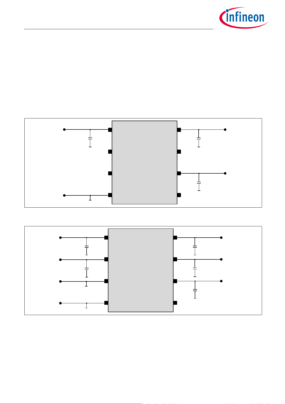
1 Application Circuits
The application circuits in this chapter show the various connection possibilities of the TLE5501. It can be used
in a single ended mode (only one sine and one cosine signal, Figure 1 and Figure 3) and in a differential mode
with a total of four output signals (Figure 2 and Figure 4).
To fully implement the safety concept of the TLE5001 E0002 version and achieve highest diagnostic coverage,
the four output signals have to be sampled singled ended. This is necessary, as the proposed external safety
mechanisms in the Safety Manual act on the single ended signals. Nevertheless, to reach highest angle
accuracy, the differential calculated angle shall be used for the application. The single ended signals are for
diagnostic only.
Figure 1 Application circuit for TLE5501 E0001 single ended signal used
Figure 2 Application circuit for TLE5501 E0001 differential signal used
User’s Manual 3 Rev. 1.0
2019-04-29
Page 4
TLE5501
SIN_P
VDD_P
COS_P
GND_P
COS_N
SIN_N
GND_N
TLE5501
VDD_N
C
b
C
b
10 0n
SIN_P
VDD_P
COS_P
GND_P
SIN_P
VDD_P
COS_P
GND_P
COS_N
SIN_N
GND_N
TLE5501
VDD_N
C
b
C
b
10 0n10 0n
C
b
C
b
GND_N
SIN_N
VDD_N
COS_N
SIN_P
VDD_P
COS_P
GND_P
TMR-Based Angle Sensor
Application Circuits
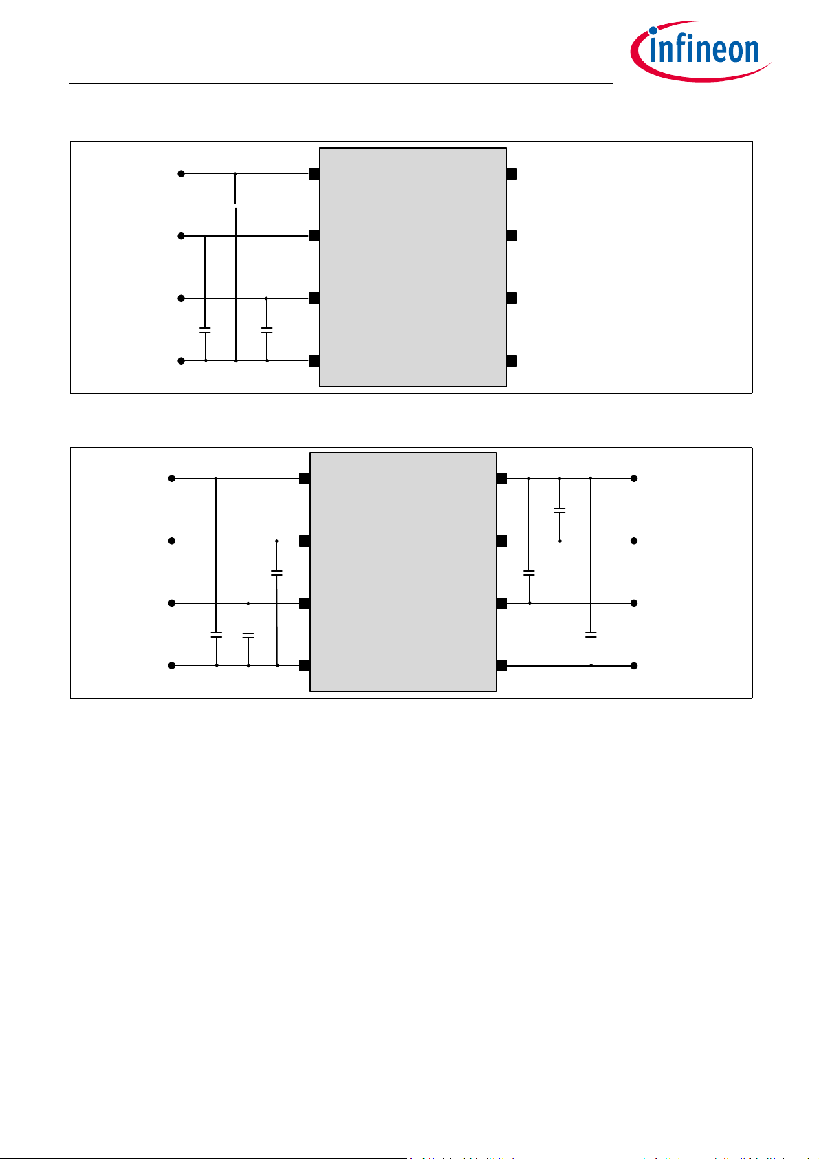
Figure 3 Application circuit for TLE5501 E0002 single ended signal used
Figure 4 Application circuit for TLE5501 E0002 differential signal used
It is recommended to use a 100nF capacitor on the VDD pin to filter noise on the supply line. As the device is
ratiometric, any noise on the supply is coupled to the sensor output.
2019-04-29
User’s Manual 4 Rev. 1.0
Page 5
TLE5501
R
TMR
GND
VDD
U_out
C
b
R
TMR
Ut() U01e–
t τ⁄–
()=
TMR-Based Angle Sensor
Transient behavior
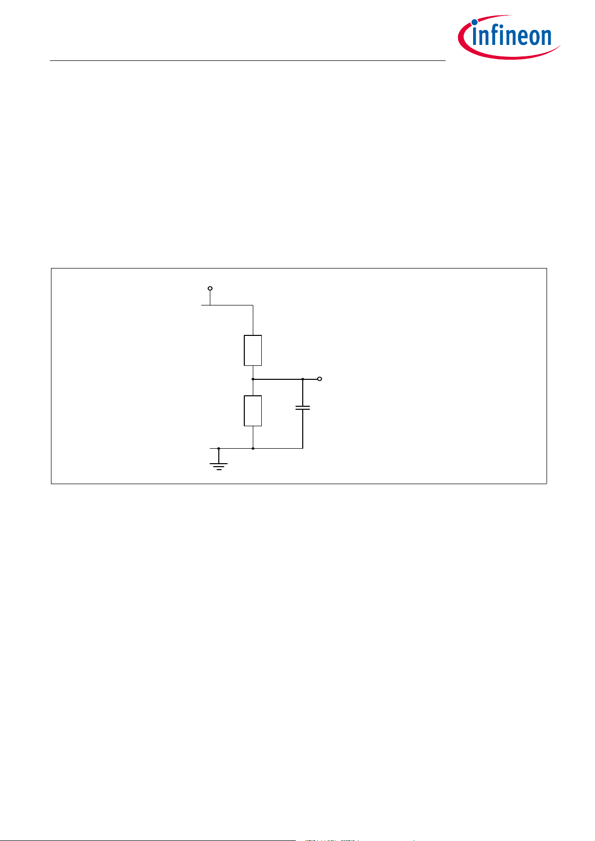
2 Transient behavior
For the sine and cosine output pins, it is also recommended to use a buffer capacitor Cb for filtering purpose.
As the device itself has a high output impedance, given by the TMR resistors R
a low-pass filter together with the bridge resistivity.
2.1 Bandwidth of the TMR bridge
It has to be taken into account that the low pass filter limits the bandwidth of the sensor and increases step
response time. Figure 5 shows a schematic of the sensor output structure with an external capacitor C
resistivity of a TMR resistor R
is specified in the datasheet and has a value between 4kΩ and 8kΩ.
TMR
, this buffer capacitor builds
TMR
. The
b
Figure 5 Schematic of one branch of the TMR bridge with external buffer capacitor C
The result of a pSPICE simulation of this output structure is shown in Figure 6. A resistor of R
capacitor value of C
= 1nF is assumed. Applying a voltage step of 5V on the supply VDD is simulated. This is
b
b
= 8kΩ and a
TMR
compared with analytical simulations using below Equation (2.1):
(2.1)
The time constant for the bridge τ
is defined as: τbr = RC, U0 is taken to be 2.5V = VDD/2.
br
A good approximation of the transient behavior in the analytical calculation can be achieved with R = 4kΩ and
C
= 1nF, so R in the analytical simulation is half of the resistivity of one TMR resistor R
b
This behavior is equal to a low-pass filter at the sensor output with R = R
/2 and Cb.
TMR
of the bridge.
TMR
User’s Manual 5 Rev. 1.0
2019-04-29
Page 6

TLE5501
0.00
0.50
1.00
1.50
2.00
2.50
3.00
0.0E+00 5.0E-06 1.0E-05 1.5E-05 2.0E-05 2.5E-05 3.0E-05 3.5E-05
U_ou t (V)
time (s)
pSPICE
analyt. R = 4k
analyt. R = 8k
Ut()
U
0
-----------
X
c
R2X
c
2
+
--------------------------
Xc,
1
2πfC⋅
-----------------
==
Phase arc 2πfRC()tan–=
TMR-Based Angle Sensor
Transient behavior
Figure 6 Simulation (pSPICE and analytical) of the RC behavior of the output voltage (R
= 1nF). Voltage step on V
. The 100nF capacitor on VDD is not included in the simulations
DD
= 8kΩ, Cb
TMR
The transient behavior when applying an AC magnetic field with frequency f is shown in Figure 7 and Figure 8.
The pSPICE simulation is compared with analytical calculations according to Equation (2.2) and
Equation (2.3) below. Again, a good fit is achieved using R = 4kΩ for the calculation.
(2.2)
(2.3)
User’s Manual 6 Rev. 1.0
2019-04-29
Page 7

TLE5501
0.00
0.10
0.20
0.30
0.40
0.50
0.60
0.70
0.80
0.90
1.00
100 1000 10000 100000
U(t)/U0
frequency (Hz)
Ampl. pSPICE
Ampl. analyt.
-90
-80
-70
-60
-50
-40
-30
-20
-10
0
100 1000 10000 100000
Phase (°)
frequency (Hz)
Phase pSPICE
Phase analyt.
TMR-Based Angle Sensor
Transient behavior
Figure 7 Normalized output amplitude for an AC magnetic field excitation. Bridge resistor R
8kΩ, C
=1nF. For the analytical calculation, the values R = 4kΩ and Cb = 1nF are used
b
(Equation (2.2))
TMR
=
Figure 8 Phase shift between output signal and excitation for an AC magnetic field. Bridge resistor
= 8kΩ, Cb =1nF. For the analytical calculation, the values R = 4kΩ and Cb = 1nF are used
R
The transient behavior of the TMR output can be approximated with a simple RC model, using R = R
User’s Manual 7 Rev. 1.0
TMR
(Equation (2.3))
/2.
TMR
2019-04-29
Page 8

TLE5501
f
c
1
2πRC
---------------
1
πR
TMR
C
--------------------------
39.78kHz== =
f
Φ()tan
2πRC
-----------------
=
Ut() U
0
1e–
t τ⁄–
()⋅ U
0
1
0.5
2
N
-------
–
èø
æö
⋅==
TMR-Based Angle Sensor
Transient behavior
For a bridge resistivity of R
according to Equation (2.4) with R = R
= 8kΩ and a buffer capacitor of Cb = 1nF, the cut-off frequency fc is calculated
TMR
/2.
TMR
(2.4)
Care should be taken, that the buffer capacitor C
is chosen in a way that the phase shift between output signal
b
and input signal does not impact the angle accuracy for the maximum given frequency in the application.
For example, to have the phase shift Φ below 0.2° with a C
= 1nF, the maximum frequency f
b
rotation
in the
application is estimated according Equation (2.5) to be below 139Hz = 8340rpm.
(2.5)
As the TLE5501 is a passive sensor with analog output, also further capacitive load, coming e.g. from the ADC
input of the microcontroller has to be considered. Further details to that are given in Chapter 3. The operation
of the TLE5501 should always be well below the calculated cut-off frequency f
considered (buffer capacitor C
according to the datasheet. Depending on the accuracy requirements of the application, it might be
R
TMR
, ADC input capacity, parasitics) and assuming a worst case bridge resistivity
b
with the total capacitive load
c
necessary to further reduce the input magnetic frequency to minimize the phase shift between input and
output signal to the required value.
Settling time τ
of a RC filter
s
Assuming an ADC with N bits resolution, which is used to measure the bridge output signal, it is desired that
the measurement error of the output voltage is less than 0.5LSB.
To achieve this, the input frequency has to be low compared to the cut-off frequency f
by the RC time constant τ
of the bridge resistivity and the external capacitor.
br
Using Equation (2.1), the following relation can be obtained for the time until the voltage reaches U
(Equation (2.4)), given
c
with a
0
deviation of less than 0.5LSB:
(2.6)
User’s Manual 8 Rev. 1.0
2019-04-29
Page 9

TLE5501
τ
s
τ
b
r
0.5
2
N
-------
èø
æö
ln⋅
èø
æö
–=
C
b
Φ()tan
2πRf
in
-----------------
=
TMR-Based Angle Sensor
Transient behavior
For the time τ
until the voltage settles to a value less than 0.5LSB from final value U0 the following relation
s
holds:
(2.7)
For a 12 bit ADC with N = 12, τ
This means that a waiting time of approx. 9 times of τ
becomes τs = 9.0τbr.
s
should be considered for settling the signal before it
br
can be converted with the ADC.
2.2 Recommendation for the external capacitor C
b
For most applications, it is a target to achieve a high angle accuracy. To reach this, the phase shift Φ between
the magnetic input signal and the bridge output shall be small. It can be estimated using Equation (2.3).
The external buffer capacitor C
can be calculated depending on magnetic input frequency fin and desired
b
phase shift Φ according to Equation (2.8):
(2.8)
For an application with 8000rpm, f
maximum buffer capacitor C
The time constant τ
of the bridge in this case is τbr = R
br
is calculated to Cb = 1nF.
b
So the settling time of the bridge τ
For applications with higher speed, the buffer capacitor C
= 133Hz, R = 4kOhm (R = R
in
/2 x Cb = 4kOhm x 1nF = 4µs.
TMR
is then τs = 9τbr = 36µs.
s
b
/2, see Chapter 2.1) and Φ = 0.2° the
TMR
can be further reduced but it has to be taken into
account, that there is also a capacitive load of the ADC of the microcontroller which needs to be charged.
Further details in Chapter 3.
User’s Manual 9 Rev. 1.0
2019-04-29
Page 10

TLE5501
GND
U
ADC
C
SH
R
SH
S/H
TMR-Based Angle Sensor
Connection to a micro controller
3 Connection to a micro controller
The following chapters give some hints which should be considered when the TLE5501 is connected to a
microcontroller.
3.1 Sigma-Delta ADC
In a Sigma-Delta ADC, the analog input signal is converted into a bit stream with the bit density corresponding
to the analog input value. The sampling frequency is much higher (~MHz) than the signal frequency. A
decimation filter converts the bit stream into a digital word (demodulation).
This type of ADC has typically a high input resistivity which makes it ideally suited for connection to a high
impedance current source. Very low input currents are drawn which do not influence the sensor output
voltage. Also, high resolution can be achieved which, however, comes together with a larger delay of the
signal.
Difficult for this type of ADC is the synchronization of the sine and cosine channel, which is mandatory to
achieve a high angle accuracy. To implement the proposed safety mechanisms for the TLE5501, it is also
required to sample the single ended signals SIN_P, SIN_N, COS_P, COS_N. This makes single ended ADC
channels necessary. The four channels should be sampled synchronous or with a very low time difference.
If the microcontroller in use allows to implement the above described requirements, a Sigma-Delta ADC is a
good choice for the connection to the TLE5501.
3.2 SAR ADC
The SAR (successive approximation register) is a widely used ADC and available on most micro controllers. Its
input is a switched capacitor structure with a sample and hold circuit. It supports a fast sampling frequency
with a typical resolution of 10 to 12 bits.
Figure 9 shows an input structure of an SAR ADC. In the “sample” phase, the S/H switch is closed and the
“sample and hold” capacitor C
switch S/H is opened and the voltage stored in C
required for charging the capacitor and conversion to a digital value is called conversion time.
is charged via the resistor RSH (sampling time). After the sampling time the
SH
is converted to a digital value (hold time). The total time
SH
Figure 9 Schematic input structure of an SAR ADC.
The high output impedance of the TMR bridge together with the external buffer capacitor C
considerable impact on the timing behavior of the SAR ADC. An equivalent circuit is shown in Figure 10.
User’s Manual 10 Rev. 1.0
2019-04-29
has a
b
Page 11

TLE5501
GND
U
ADC
C
SH
R
SH
S/H
R
TMR
GND
VDD
C
b
R
TMR
TMR bridge
ADC
ΔUU
0
C
S
H
CbCSH+()
------------------------------
=
TMR-Based Angle Sensor
Connection to a micro controller
Figure 10 Equivalent circuit of TMR bridge (only half bridge is shown) and SAR ADC input
3.2.1 Load step
The following consideration is made with the initial condition that the buffer capacitor Cb is fully charged, the
S/H switch is open and the sample and hold capacitor C
/2 and the voltage U
V
DD
ADC
= 0V.
When the S/H switch is closed, charge is flowing from C
, increases. In addition, charge is flowing from the supply voltage VDD via the TMR resistor R
U
ADC
C
.
b
The following parameters are assumed: V
The time constant τ
For charging C
charging of C
is much faster (~ 9x14ns = 140ns) than the recovery of the voltage at Cb (~ 9x4µs = 36µs).
b
for charging Cb via R
br
the time constant τSH = RSH x CSH = 14ns. Therefore, the charging of CSH and also the de-
SH
Due to this, with the assumption that τ
approximated as follows (Equation (3.1)):
= 5V, R
DD
TMR
>> τ
br
TMR
is given by τbr = R
the voltage at Cb drops by a value of ΔU which can be
SH
is decharged. In this condition, the voltage at Cb is
SH
to CSH, the voltage at Cb drops and the voltage at CSH,
b
to charge
TMR
= 8kΩ, Cb = 1nF, RSH =2kΩ, and CSH = 7pF.
/2 x Cb = 4µs (see also Chapter 2.2).
TMR
(3.1)
With above parameters and U
bridge defines how long it takes until the voltage U
= 2.5V, the load step is calculated to ΔU = 17.4mV. The time constant τbr of the
0
is settled with sufficient accuracy (error less than
ADC
0.5LSB). Therefore, the sampling time (time for which S/H switch has to be closed) must be larger than
9 x τ
= 9x4µs = 36µs.
br
Figure 11 shows this behavior. At t = 1µs the S/H switch is closed and remains so until t = 37µs. In the first
moment, the voltage drops by ΔU = 17mV and then increases with the time constant of the bridge τ
User’s Manual 11 Rev. 1.0
= 4µs.
br
2019-04-29
Page 12

TLE5501
2.480
2.485
2.490
2.495
2.500
2.505
2.510
0.0 10.0 20.0 30.0 40.0 50.0
U (V)
time (µs)
U @ Cb
U_ADC
CSH discharged
Load step ΔU
hold time
S/H switch open
sampling time
S/H switch closed
f
sample
1
9 τbr⋅
---------------
<
TMR-Based Angle Sensor
Connection to a micro controller
After 36µs the capacitors C
and Cb are almost fully charged, the S/H switch is opened and the ADC can start
SH
with the conversion and will sample the correct voltage of V
discharged and the next sampling phase starts.
/2. After the hold time the capacitor CSH is
DD
Figure 11 Sampling and conversion of the TMR bridge signal with a SAR ADC.
The time constant of the bridge τ
f
. In above example the maximum sampling frequency is estimated to f
sample
br
= R
/2 x Cb is determining the maximum possible sampling frequency
TMR
~ 27.7kHz (Equation (3.2))
sample
In reality, the achievable sampling frequency is lower, as also some additional time has to be included for the
hold time of the ADC. Sampling time and hold time are depending on the settings of the microcontroller in use.
The relation between buffer capacitor C
Figure 12. In this calculation, sensor bandwidth f
, sampling frequency f
b
is calculated assuming that the phase shift Φ between
rotation
and sensor bandwidth f
sample
rotation
external magnetic field and electrical sine/cosine output signal is less than 0.2° according to Equation (2.5).
R
is assumed to be 8kΩ.
TMR
(3.2)
is shown in
User’s Manual 12 Rev. 1.0
2019-04-29
Page 13

TLE5501
100
1000
10000
100000
1
10
100
1,000
0.0 0.1 1.0 10.0 100.0
f_rotation (rpm)
f_sample (kHz)
Cb(nF)
f_sample
f_rotation
C
b
2
N1+
1–()C
S
H
⋅>
TMR-Based Angle Sensor
Connection to a micro controller
Figure 12 Sampling frequency f
. R
C
b
is assumed to be 8kΩ.
TMR
and sensor bandwidth f
sample
as function of the buffer capacitor
rotation
3.2.2 Load step reduction
As seen in Equation (3.1), the drop of the voltage at the start of the ADC sampling (closing of S/H switch) can
be reduced by increasing the value of C
is no need for a dedicated waiting time until the signal settles. Using Equation (3.1) the following relation can
be obtained (N: bits of the ADC):
For a 12bit ADC and C
= 7pF, the buffer capacitor Cb has to be larger than 57.3nF. In this case, the voltage drop
SH
during ADC sampling is less than 0.5 LSB and therefore not visible.
On the other side, such a large buffer capacitor limits the bandwidth of the sensor and the time constant of the
bridge calculates to τ
applied magnetic field f
= 229.3µs. For the phase shift to be less than 0.2°, the maximum frequency of the
br
has to be below 145rpm according to Equation (2.5).
rotation
In this approach, the sampling frequency can be increased but the bandwidth of the sensor is reduced at the
same time.
. If this load step ΔU is less than 0.5 LSB , it is no longer visi ble a nd there
b
(3.3)
For a specific application, the best combination of required bandwidth, sampling frequency and sampling
accuracy has to be found and the buffer capacitor C
User’s Manual 13 Rev. 1.0
has to be selected accordingly.
b
2019-04-29
Page 14

TLE5501
2.460
2.465
2.470
2.475
2.480
2.485
2.490
2.495
2.500
2.505
0.0 1.0 2.0 3.0 4.0 5.0 6.0 7.0 8.0
U (V)
time (µs)
U @ Cb
U_ADC
hold time
S/H switch open
sampling time
S/H switch closed
TMR-Based Angle Sensor
Connection to a micro controller
3.2.3 Oversampling
As seen in Chapter 3.2.1 the sampling frequency f
is mainly given by the buffer capacitor Cb. In some
sample
cases, it might be necessary to perform an oversampling, i.e. to measure the same value several times and
calculate the average to increase resolution. Figure 13 shows an extreme condition with C
time of 1µs and a hold time of 1µs, giving a total conversion time of 2µs. In this case the buffer capacitor C
= 1nF, a sampling
b
is
b
not full charged as the time constant of the bridge is much larger than the sampling time. After each sampling
step, the voltage drops further and can not fully recover in the following hold time.
Figure 13 ADC voltage for a sampling time of 1µs and a conversion time of 1µs
As a consequence, the measured sine and cosine output voltage has an error which can contribute to an
additional angle error. As long as it is a constant and stable condition, this amplitude error is compensated
when doing the sensor calibration (matching of sine and cosine amplitude). Furthermore, as only the ratio of
sine and cosine amplitude is relevant for the angle calculation, a part of this error is canceled.
Nevertheless, the user has to verify in the specific application, whether the selected oversampling parameters
(sampling time and hold time), together with the external circuitry meets the requirements in angle accuracy.
User’s Manual 14 Rev. 1.0
2019-04-29
Page 15

TLE5501
15
20
25
30
35
40
45
50
55
60
65
70
75
80
85
-50-250 255075100125150
B (mT)
T (°C)
TMR-Based Angle Sensor
Calibration
4 Calibration
Before the TLE5501 can be used in an application, a calibration on system level has to be performed. The four
analog output signals SIN_P, SIN_N, COS_P, COS_N have usually an offset and an amplitude mismatch. This
has to be corrected before the angle can be calculated. Also, SIN and COS output signals have an orthogonality
error, means that they are not precisely 90° phase shifted. This needs also to be compensated to achieve the
accuracy specified in the datasheet. The calibration has to be done for all single ended signals which are
intended to be used. In case the differential signals are used, there must also be a compensation based on the
differential signals. Further details how to perform the calibration is described in the Application Note
“TLE5xxx(D)_Calibration_360”. Usually this calibration is performed at 25°C and at 0h.
The sensor TLE5501 is intended to be used with a specified magnetic field strength, which range is specified
in the datasheet. It has to be ensured that the device is not exposed to a magnetic field outside the specified
range over the whole temperature and lifetime range. Also the temperature characteristics of the magnet in
use has to be considered. For the usual magnet material, the magnetic field strength is reduced with
increasing temperature and increased with decreasing temperature. Therefore, depending on the maximum
and minimum temperatures in the application, the magnetic field at 25°C and 0h has to be adjusted
accordingly in order not to violate the specified limits. Given a specified range of 25mT to 80mT for the allowed
magnetic field range and considering a ferrite magnet material with Tc = -2000ppm/K, the magnetic field in the
whole temperature range will be as shown as in Figure 14.
Figure 14 Magnetic field for a ferrite magnet with TC = -2000ppm/K in the full temperature range.
Specified minimum and maximum field values of 25mT and 80mT are considered.
Different magnet material leads to a different temperature characteristic of the magnetic field. This has to be
taken into account by the user of the device.
To achieve the specified angle accuracy of TLE5501, it has to be ensured that the magnetic field during lifetime
and temperature range of the application does not deviate too much from the initial calibration condition at
25°C/B
This condition is met when the deviation of B
variations) is less than 10%.
User’s Manual 15 Rev. 1.0
/0h. B0 is the magnetic field at initial calibration condition at 25°C/0h.
0
over lifetime (due to e.g. aging of magnet and mechanical airgap
0
2019-04-29
Page 16

TLE5501
15
20
25
30
35
40
45
50
55
60
65
70
75
80
85
-50 -25 0 25 50 75 100 125 150
B (mT)
T (°C)
B_tol,max
B_tol,min
Calibration @25°C
Bmin
Bmax
TMR-Based Angle Sensor
Calibration
Therefore, the following relation has to be ensured by the user over the complete lifetime:
B
= 0.9B0 < B < 1.1B0 = B
min
magnetic field at initial calibration condition (25°C) over lifetime
; with B0: magnetic field at 25°C/0h and B
max
min
, B
: minimum and maximum
max
The temperature behavior of B
min
and B
is given by the temperature coefficient of the magnet material.
max
An example for an initial calibration point at 25°C/50mT/0h is shown in Figure 15.
Figure 15 One-time calibration a 25°C/50mT. Dashed lines show the allowed magnetic field range
taking into account the temperature effect and aging of the magnet. Assumptions: ferrite
magnet material with TC = -2000ppm/K, 10% field strength variation from initial calibration
condition (25°C/50mT) over lifetime.
Figure 16 shows the typical angle error for a sensor which has its initial calibration of offset, amplitude and
orthogonality error at 25°C/50mT. Due to aging effects of the magnet, it is assumed that the magnetic field at
25°C is reduced by 10% to 45mT. The sensor is still operated with calibration parameters coming from initial
calibration at 25°C/50mT, thus having no longer optimized calibration values. Over temperature, the magnetic
field is changing with a T
of -2000pm/K (ferrite magnet material is assumed). This means that the magnetic
C
field at the sensor deviates more or less (depending on temperature) from the initial calibration condition B
= 50mT. This deviation causes an angle error which is shown in Figure 16.
User’s Manual 16 Rev. 1.0
0
2019-04-29
Page 17

TLE5501
0.1
0.15
0.2
0.25
0.3
0.35
-50 -25 0 25 50 75 100 125 150 175
angle error (°)
temperature (°C)
50mT
Initial calibration
50.8mT
49.1mT
47.2mT
45.0mT
42.8mT
39.6mT
36.0mT
33.8mT
TMR-Based Angle Sensor
Calibration
Figure 16 Typical angle error with initial calibration at 25°C/50mT and subsequent measurements
considering 10% magnetic field change due to aging and air gap variation (i.e. 45mT @25°C).
Magnetic field values change with a TC of -2000ppm/K (ferrite magnet material). Magnetic
field values are indicated at each measurement temperature.
User’s Manual 17 Rev. 1.0
2019-04-29
Page 18

TLE5501
TMR-Based Angle Sensor
Revision History
5 Revision History
Revision Date Changes
0.1 2019-04-29 Initial version
User’s Manual 18 Rev. 1.0
2019-04-29
Page 19

Trademarks of Infineon Technologies AG
All referenced product or service names and trademarks are the property of their respective owners.
IMPORTANT NOTICE
Edition 2019-04-29
Published by
Infineon Technologies AG
81726 Munich, Germany
© 2019 Infineon Technologies AG.
All Rights Reserved.
Do you have a question about any
aspect of this document?
Email: erratum@infineon.com
Document reference
The information contained in this application note is
given as a hint for the implementation of the product
only and shall in no event be regarded as a description
or warranty of a certain functionality, condition or
quality of the product. Before implementation of the
product, the recipient of this application note must
verify any function and other technical information
given herein in the real application. Infineon
Technologies hereby disclaims any and all warranties
and liabilities of any kind (including without limitation
warranties of non-infringement of intellectual
property rights of any third party) with respect to any
and all information given in this application note.
The data contained in this document is exclusively
intended for technically trained staff. It is the
responsibility of customer’s technical departments to
evaluate the suitability of the product for the intended
application and the completeness of the product
information given in this document with respect to
such application.
For further information on technology, delivery terms
and conditions and prices, please contact the nearest
Infineon Technologies Office (www.infineon.com).
WARNINGS
Due to technical requirements products may contain
dangerous substances. For information on the types
in question please contact your nearest Infineon
Technologies office.
Except as otherwise explicitly approved by Infineon
Technologies in a written document signed by
authorized representatives of Infineon Technologies,
Infineon Technologies’ products may not be used in
any applications where a failure of the product or any
consequences of the use thereof can reasonably be
expected to result in personal injury.
 Loading...