

Page 1
Data Sheet Rev. 1.1
www.infineon.com 1 2019-04-04
TLE5014SP16 E0002
GMR-based Angle Sensor
Features
• Fast SSC interface up to 8MHz
• Giant Magneto Resistance (GMR)-based principle
• Integrated magnetic field sensing for angle measurement
• 360° angle measurement
• EEPROM for storage of configuration (e.g. zero angle) and customer
specific ID
• 15 bit representation of absolute angle value on the output
• Max. 1° angle error over lifetime and temperature range
• Developed according to ISO26262 with process complying to ASIL-D
• Internal safety mechanisms with a SPFM > 97%
• 32 point look-up table to correct for systematic angle errors (e.g. magnetic circuit)
• 112 bit customer ID (programmable)
• Automotive qualified Q100, Grade 1: -40°C to 125°C (ambient temperature)
•ESD: 4 kV (HBM) on V
• RoHS compliant and halogen free package
and 2kV (HBM) on output pins
DD
Functional Safety
Safety Manual and Safety Analysis Summary Report available on request
Product validation
Qualified for automotive applications. Product validation according to AEC-Q100.
Description
The TLE5014SP16 E0002 is an iGMR (integrated GMR) based angle sensor with a high speed serial interface
(SSC interface). It provides high accurate angular position information for various applications.
Table 1 Derivative Ordering codes
Product Type Marking Ordering Code Package Comment
TLE5014SP16 E0002 014SP02 SP004531446 PG-TDSO-16 SSC Interface, single die
Page 2

TLE5014SP16 E0002
GMR-based Angle Sensor
Table of contents
1 Functional Description . . . . . . . . . . . . . . . . . . . . . . . . . . . . . . . . . . . . . . . . . . . . . . . . . . . . . . . . . . . . 3
1.1 Block Diagram . . . . . . . . . . . . . . . . . . . . . . . . . . . . . . . . . . . . . . . . . . . . . . . . . . . . . . . . . . . . . . . . . . . . . . . . . . . . 3
1.2 Functional Block Description . . . . . . . . . . . . . . . . . . . . . . . . . . . . . . . . . . . . . . . . . . . . . . . . . . . . . . . . . . . . . . 3
1.3 Sensing Principle . . . . . . . . . . . . . . . . . . . . . . . . . . . . . . . . . . . . . . . . . . . . . . . . . . . . . . . . . . . . . . . . . . . . . . . . . 4
1.4 Pin Configuration . . . . . . . . . . . . . . . . . . . . . . . . . . . . . . . . . . . . . . . . . . . . . . . . . . . . . . . . . . . . . . . . . . . . . . . . . 6
1.5 Pin Description . . . . . . . . . . . . . . . . . . . . . . . . . . . . . . . . . . . . . . . . . . . . . . . . . . . . . . . . . . . . . . . . . . . . . . . . . . . 6
2 Application Circuits . . . . . . . . . . . . . . . . . . . . . . . . . . . . . . . . . . . . . . . . . . . . . . . . . . . . . . . . . . . . . . . 7
3 Specification . . . . . . . . . . . . . . . . . . . . . . . . . . . . . . . . . . . . . . . . . . . . . . . . . . . . . . . . . . . . . . . . . . . . 8
3.1 Absolute Maximum Ratings . . . . . . . . . . . . . . . . . . . . . . . . . . . . . . . . . . . . . . . . . . . . . . . . . . . . . . . . . . . . . . . . 8
3.2 Operating Range . . . . . . . . . . . . . . . . . . . . . . . . . . . . . . . . . . . . . . . . . . . . . . . . . . . . . . . . . . . . . . . . . . . . . . . . . 9
3.3 Electrical Characteristics . . . . . . . . . . . . . . . . . . . . . . . . . . . . . . . . . . . . . . . . . . . . . . . . . . . . . . . . . . . . . . . . . 11
3.3.1 Input/Output Characteristics . . . . . . . . . . . . . . . . . . . . . . . . . . . . . . . . . . . . . . . . . . . . . . . . . . . . . . . . . . . . 11
3.3.2 ESD Protection . . . . . . . . . . . . . . . . . . . . . . . . . . . . . . . . . . . . . . . . . . . . . . . . . . . . . . . . . . . . . . . . . . . . . . . . 14
3.3.3 Angle Performance . . . . . . . . . . . . . . . . . . . . . . . . . . . . . . . . . . . . . . . . . . . . . . . . . . . . . . . . . . . . . . . . . . . . . 15
3.4 EEPROM Memory . . . . . . . . . . . . . . . . . . . . . . . . . . . . . . . . . . . . . . . . . . . . . . . . . . . . . . . . . . . . . . . . . . . . . . . . 16
3.5 Reset Concept and Fault Monitoring . . . . . . . . . . . . . . . . . . . . . . . . . . . . . . . . . . . . . . . . . . . . . . . . . . . . . . . 16
3.6 External & Internal Faults . . . . . . . . . . . . . . . . . . . . . . . . . . . . . . . . . . . . . . . . . . . . . . . . . . . . . . . . . . . . . . . . . 16
3.7 Power Dissipation . . . . . . . . . . . . . . . . . . . . . . . . . . . . . . . . . . . . . . . . . . . . . . . . . . . . . . . . . . . . . . . . . . . . . . . 17
3.8 Device Programming . . . . . . . . . . . . . . . . . . . . . . . . . . . . . . . . . . . . . . . . . . . . . . . . . . . . . . . . . . . . . . . . . . . . . 17
4 Synchronous Serial Communication (SSC) interface . . . . . . . . . . . . . . . . . . . . . . . . . . . . . . . . . . 18
4.1 Data transmission . . . . . . . . . . . . . . . . . . . . . . . . . . . . . . . . . . . . . . . . . . . . . . . . . . . . . . . . . . . . . . . . . . . . . . . 18
4.1.1 Bit Numbering . . . . . . . . . . . . . . . . . . . . . . . . . . . . . . . . . . . . . . . . . . . . . . . . . . . . . . . . . . . . . . . . . . . . . . . . . 18
4.1.2 Update of update-registers . . . . . . . . . . . . . . . . . . . . . . . . . . . . . . . . . . . . . . . . . . . . . . . . . . . . . . . . . . . . . 18
4.2 Data transfer . . . . . . . . . . . . . . . . . . . . . . . . . . . . . . . . . . . . . . . . . . . . . . . . . . . . . . . . . . . . . . . . . . . . . . . . . . . . 20
4.2.1 Command Word . . . . . . . . . . . . . . . . . . . . . . . . . . . . . . . . . . . . . . . . . . . . . . . . . . . . . . . . . . . . . . . . . . . . . . . 20
4.2.2 Safety word . . . . . . . . . . . . . . . . . . . . . . . . . . . . . . . . . . . . . . . . . . . . . . . . . . . . . . . . . . . . . . . . . . . . . . . . . . . 21
4.2.3 Cyclic Redundancy Check (CRC) . . . . . . . . . . . . . . . . . . . . . . . . . . . . . . . . . . . . . . . . . . . . . . . . . . . . . . . . . 22
5 Package Information . . . . . . . . . . . . . . . . . . . . . . . . . . . . . . . . . . . . . . . . . . . . . . . . . . . . . . . . . . . . . 23
5.1 Package Parameters . . . . . . . . . . . . . . . . . . . . . . . . . . . . . . . . . . . . . . . . . . . . . . . . . . . . . . . . . . . . . . . . . . . . . 23
5.2 Package Outline . . . . . . . . . . . . . . . . . . . . . . . . . . . . . . . . . . . . . . . . . . . . . . . . . . . . . . . . . . . . . . . . . . . . . . . . . 25
5.3 Footprint . . . . . . . . . . . . . . . . . . . . . . . . . . . . . . . . . . . . . . . . . . . . . . . . . . . . . . . . . . . . . . . . . . . . . . . . . . . . . . . 26
5.4 Packing . . . . . . . . . . . . . . . . . . . . . . . . . . . . . . . . . . . . . . . . . . . . . . . . . . . . . . . . . . . . . . . . . . . . . . . . . . . . . . . . . 26
5.5 Marking . . . . . . . . . . . . . . . . . . . . . . . . . . . . . . . . . . . . . . . . . . . . . . . . . . . . . . . . . . . . . . . . . . . . . . . . . . . . . . . . . 27
6 Revision history . . . . . . . . . . . . . . . . . . . . . . . . . . . . . . . . . . . . . . . . . . . . . . . . . . . . . . . . . . . . . . . . . 28
Data Sheet 2 Rev. 1.1
2019-04-04
Page 3
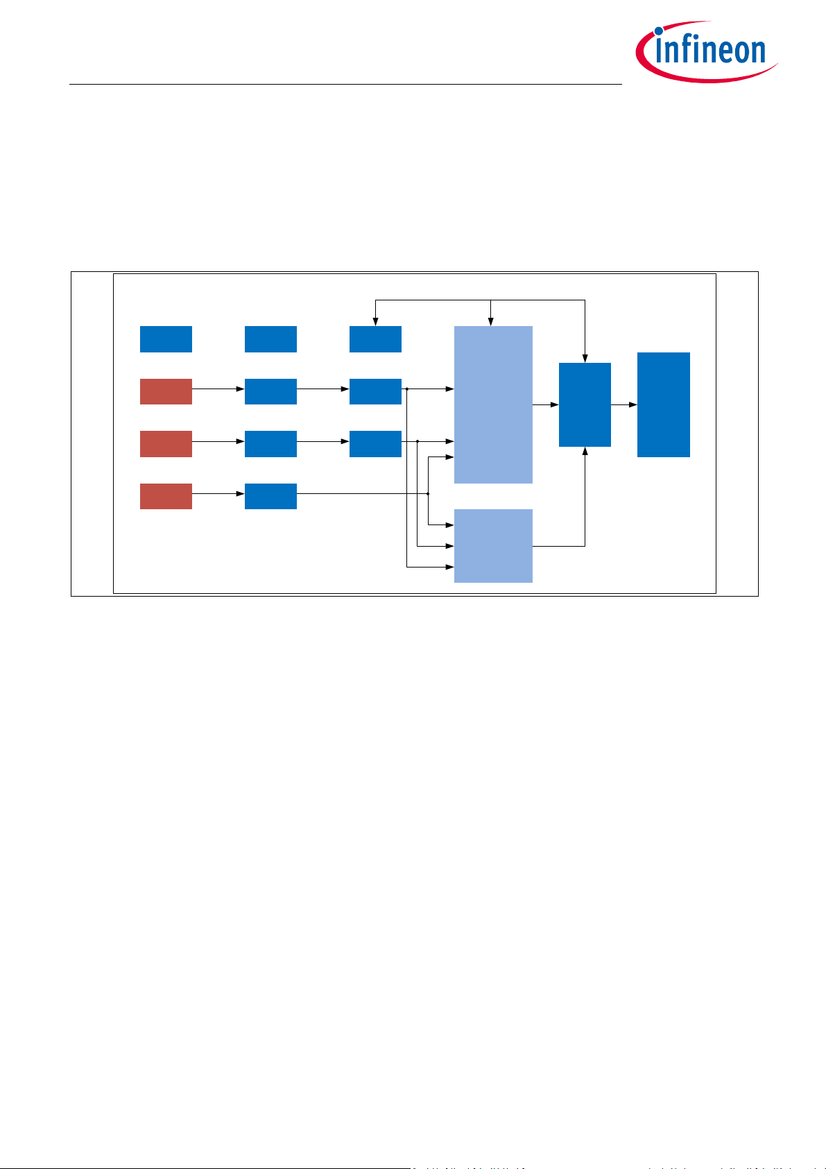
PMU Clock EEPROM
ADC_X Filter
ADC_Y Fil ter
GMR_X
GMR_Y
Temp. ADC_T
ISM_ALG
CORDIC
(Hardware)
SSC
Interface
ISM_SAF
CORDIC
(Software)
Interface
compare
TLE5014SP16 E0002
GMR-based Angle Sensor
Functional Description
1 Functional Description
1.1 Block Diagram
Figure 1-1 TLE5014SP16 E0002 block diagram
1.2 Functional Block Description
Internal Power Supply (PMU)
The internal blocks of the TLE5014SP16 E0002 are supplied from several voltage regulators:
• GMR Voltage Regulator, VRS
• Analog Voltage Regulator, VRA
• Digital Voltage Regulator, VRD
These regulators are directly connected to the supply voltage VDD.
Oscillator and PLL (Clock)
The digital clock of the TLE5014SP16 E0002 is given by the Phase-Locked Loop (PLL), which is fed by an
internal oscillator.
SD-ADC
The Sigma-Delta Analog-Digital-Converters (SD-ADC) transform the analog GMR voltages and temperature
voltage into the digital domain.
Digital Signal Processing Unit ISM_ALG
The Digital Signal Processing Unit ISM_ALG contains the:
• Intelligent State Machine (ISM), which does error compensation of offset, offset temperature drift,
amplitude synchronicity and orthogonality of the raw signals from the GMR bridges.
• COordinate Rotation DIgital Computer (CORDIC), which contains the trigonometric function for angle
calculation
Data Sheet 3 Rev. 1.1
2019-04-04
Page 4

TLE5014SP16 E0002
GMR-based Angle Sensor
Functional Description
Digital Signal Processing Unit ISM_SAF
The Digital Signal Processing Unit ISM_SAF performs the internal safety mechanism and plausibility checks.
Furthermore, a second CORDIC algorithm is implemented in a diverse way as in the ISM_ALG. This is for cross
checking the angle calculation
Interface
The Interface block is used to generate the SSC signals
Angle Compare
This digital block compares the angle value calculated by ISM_ALG and ISM_SAF. In case they are not identical,
an error is indicated in the transmitted protocol.
EEPROM
The EEPROM contains the configuration and calibration parameters. A part of the EEPROM can be accessed by
the customer for application specific configuration of the device. Programming of the EEPROM is achieved
with the SSC interface. Programming mode can be accessed directly after power-up of the IC.
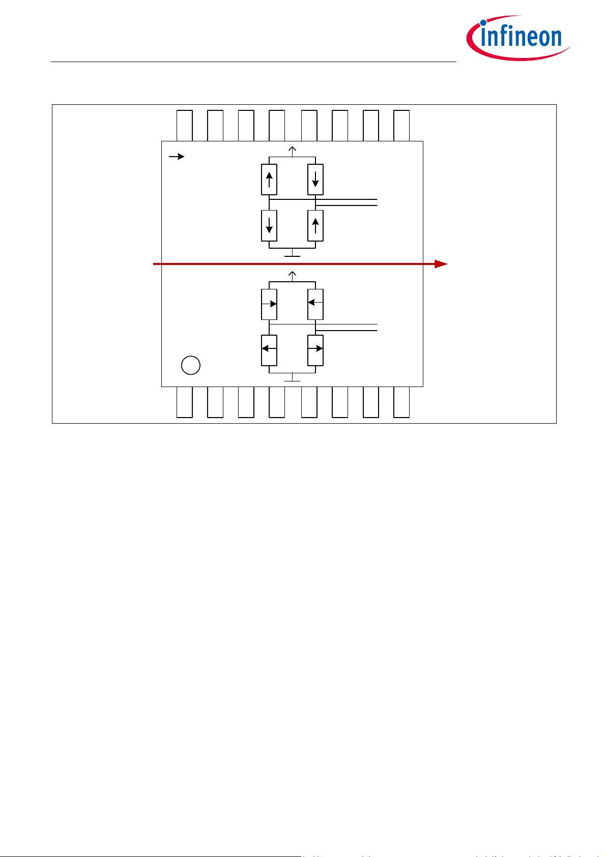
1.3 Sensing Principle
The Giant Magneto Resistance (GMR) sensor is implemented using vertical integration. This means that the
GMR-sensitive areas are integrated above the logic part of the TLE5014SP16 E0002 device. These GMR
elements change their resistance depending on the direction of the magnetic field.
Four individual GMR elements are connected to one Wheatstone sensor bridge. These GMR elements sense
one of two components of the applied magnetic field:
•X component, V
•Y component, V
With this full-bridge structure the maximum GMR signal is available and temperature effects cancel out each
other.
(cosine) or the
x
(sine)
y
Data Sheet 4 Rev. 1.1
2019-04-04
Page 5
0°
10111213141516
1
9
87654321
Reference Direction:
Resist anc e low when
external magnetic field is
in this direction
Y
X
TLE5014SP16 E0002
GMR-based Angle Sensor
Functional Description
Figure 1-2 Sensitive bridges of the GMR sensor (not to scale)
In Figure 1-2 the arrows in the resistors represent the magnetic direction which is fixed in the reference layer.
If the external magnetic field is parallel to the direction of the Reference Layer, the resistance is minimal. If
they are anti-parallel, resistance is maximal.
The output signal of each bridge is only unambiguous over 180° between two maxima. Therefore two bridges
are oriented orthogonally to each other to measure 360°.
With the trigonometric function ARCTAN2, the true 360° angle value is calculated out of the raw X and Y signals
from the sensor bridges.
Data Sheet 5 Rev. 1.1
2019-04-04
Page 6
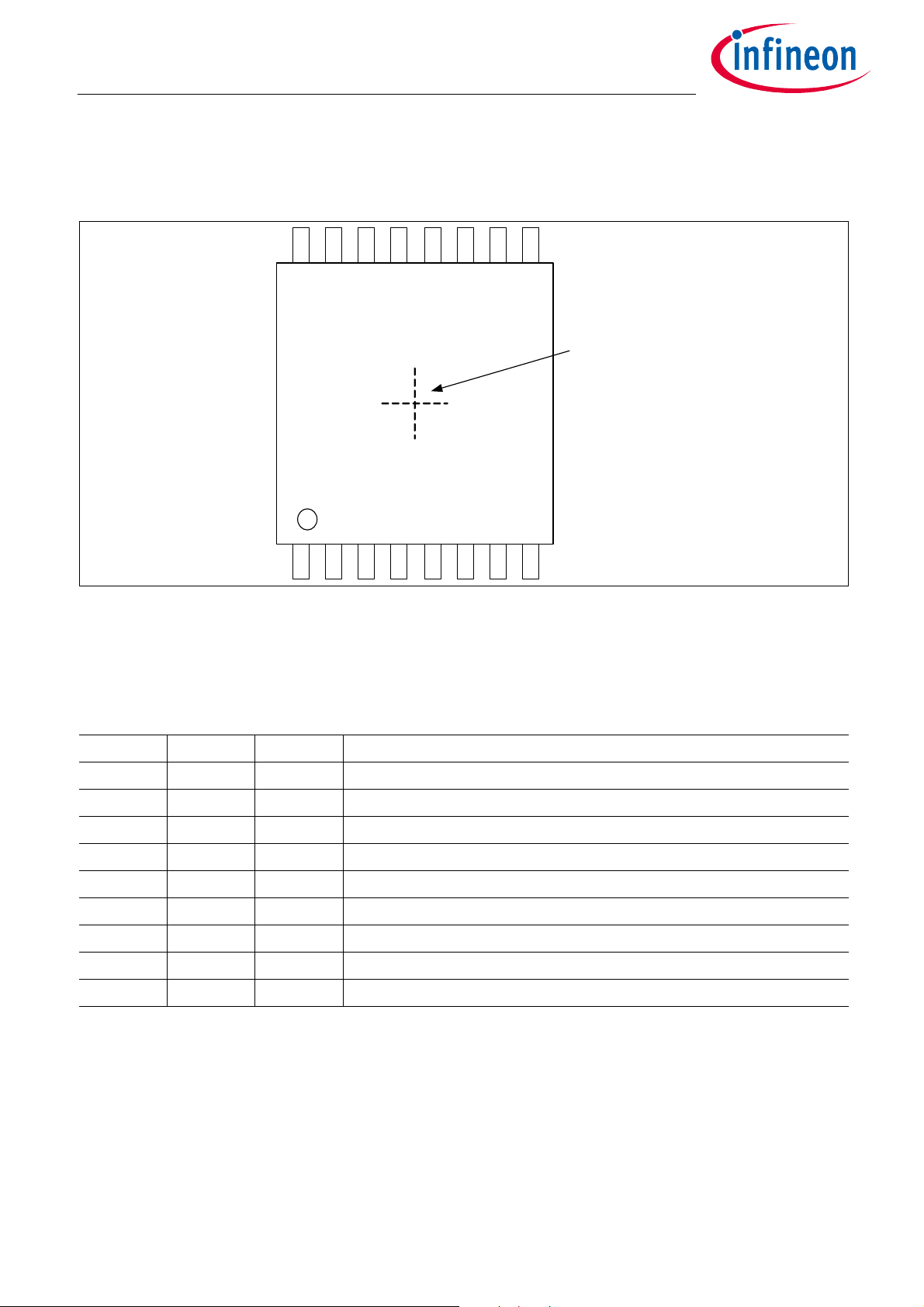
10111213141516
1
9
87654321
Center of
Sensitive area
TLE5014SP16 E0002
GMR-based Angle Sensor
Functional Description
1.4 Pin Configuration
Figure 1-3 Pin configuration (top view)
1.5 Pin Description
The following Table 1-1 describes the pin-out of the chip.
Table 1-1 Pin description TLE5014SP16
Pin Symbol In/Out Function
1 IF1 I/O DATA (MOSI/MISO)
2 IF2 I SCK (SSC clock)
3 IF3 I CSQ (chip select)
4 VDD – Supply voltage, positive
5 GND – Supply voltage, ground
6 IFA – Connect to GND
7 IFB – Connect via pull-up to V
8 IFC – Keep open
9-16 - – n.c.
DD
Data Sheet 6 Rev. 1.1
2019-04-04
Page 7
µController
Master
TLE501 4
GND
10 0nF
V
DD
GND
IF1
IF2
IF3
IFA
IFB
IFC
V
µC
2.2k
50k
C
D
R
PU
R
P1
SC K
MOSI/MISO
CSQ
GND
C
L
V
DD
V
DD
V
DD
TLE5014SP16 E0002
GMR-based Angle Sensor
Application Circuits
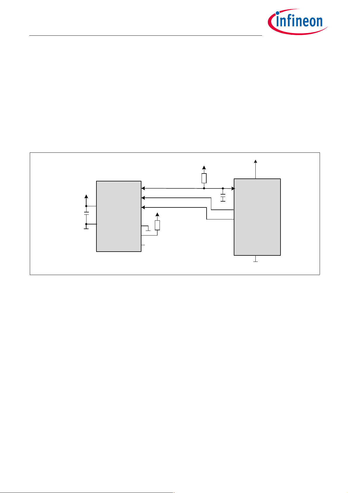
2 Application Circuits
The application circuit in this chapter shows the communication possibilities of the TLE5014SP16 E0002. To
improve robustness against electro-magnetic disturbances, a capacitor of 100nF on the supply is
recommended. This capacitor shall be placed as close as possible to the corresponding sensor pins. The load
capacitor C
but the driver is switched off once reaching the HIGH state. Therefore, a pull-up resistor is recommended to
maintain a stable HIGH level.
In case of a high speed communication, an additional serial resistor in the range of 140Ω can be implemented
in the DATA, SCK and CSQ line to avoid reflections and enhance communication reliability. In this case the user
is responsible to verify that the intended communication speed can be reached in his specific setup.
shall not exceed the specified value (Table 3-5). The DATA line is actively driven to HIGH and LOW
L
Figure 2-1 Application circuit for TLE5014SP16 E0002 with SSC interface, microcontroller switches pin
between MISO and MOSI
Data Sheet 7 Rev. 1.1
2019-04-04
Page 8
TLE5014SP16 E0002
GMR-based Angle Sensor
Specification
3 Specification
3.1 Absolute Maximum Ratings
Stresses above the max. values listed here may cause permanent damage to the device. Exposure to absolute
maximum rating conditions for extended periods may affect device reliability. Maximum ratings are absolute
ratings; exceeding only one of these values may cause irreversible damage to the device.
Table 3-1 Maximum Ratings for Voltages and Output Current
Parameter Symbol Values Unit Note / Test Condition
Min. Typ. Max.
Absolute maximum supply
voltage
Voltage Peaks V
Absolute maximum voltage
V
DD
DD
V
IF
-18 26 V for 40h, no damage of device;
-18V means V
< GND
DD
30 V for 50µs, no current limitation
-0.3 6 V no damage of device
for pin IF1, IF2, IF3
Absolute maximum voltage
V
IO
for pin IFB
Voltage Peaks (for pin IFB) V
IO
Table 3-2 Maximum Temperature and Magnetic Field
-18 19.5 V for 40h; no damage of device,
-18V means V
< GND
DD
30 V for 50µs, no current limitation
Parameter Symbol Values Unit Note / Test Condition
Min. Typ. Max.
Maximum ambient
T
A
-40 125 °C Q100, Grade 1
temperature
Maximum allowed magnetic
B 200 mT max 5 min @ T
= 25°C
A
field
Maximum allowed magnetic
B 150 mT max 5 h @ T
= 25°C
A
field
Storage & Shipment
1) 2)
T
storage
5 40 °C for dry packed devices,
Relative humidity < 90%,
storage time < 3a
1) Air-conditioning of ware houses, distribution centres etc. is not necessary, if the combination of the specified limits
of 75% R.H. and 40 °C will not be exceeded during storage for more than 10 events per year, irrespective of the
duration per event, and one of the specified limits (75 % R.H. or 40 °C) will not be exceeded for longer than 30 days
per year
2) See Infineon Application Note: “Storage of Products Supplied by Infineon Technologies”
Table 3-3 Mission Profile
Parameter Symbol Values Unit Note / Test Condition
Min. Typ. Max.
Mission Profile T
Data Sheet 8 Rev. 1.1
A,max
125 °C for 2000h
2019-04-04
Page 9
TLE5014SP16 E0002
GMR-based Angle Sensor
Specification
Table 3-4 Lifetime & Ignition Cycles
Parameter Symbol Values Unit Note / Test Condition
Min. Typ. Max.
Operating life time t
op_life
15.000 h see Table 3-3 for mission
profile
Total life time t
Ignition cycles N
1) The lifetime shall be considered as an anticipation with regard to the product that shall not extend the warranty
period
tot_life
ignition
19 a additional 2a storage time
200.000 during operating lifetime t
The device qualification is done according to AEC Q100 Grade 1 for ambient temperature range -40°C < T
1)
op_life
<
A
125°C
3.2 Operating Range
The following operating conditions must not be exceeded in order to ensure correct operation of the angle
sensor. All parameters specified in the following sections refer to these operating conditions, unless otherwise
noted. Table 3-5 is valid for -40°C < T
Table 3-5 Operating Range
Parameter Symbol Values Unit Note / Test Condition
Operating supply voltage V
Supply Voltage Slew Rate V
Operating ambient
T
temperature
< 125°C unless otherwise noted.
A
Min. Typ. Max.
DD
DD_slew
A
3.0 5.5 V -
0.1 10
-40 125 °C -
8
V/s -
Angle speed n 30000 rpm -
Capacitive output load on
C
L
––50pF
SSC interface (DATA pin)
Magnetic Field Range
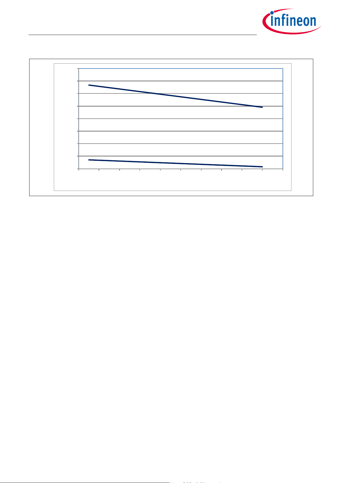
The operating range of the magnetic field describes the field values where the performance of the sensor,
especially the accuracy, is as specified in Table 3-11 and Table 3-12. This value is valid for a NdFeB magnet
with a Tc of -1300ppm/K. In case a different magnet is used, the individual Tc of this magnet has to be
considered and ensured that the limits are not exceeded. The allowed magnetic field range is given in
Figure 3-1.
Table 3-6 Magnetic Field Range
Parameter Symbol Values Unit Note / Test Condition
Min. Typ. Max.
Angle measurement field
range @ 25°C
B25 80mTT
= 25°C, valid for NdFeB
A
magnet
The below figure Figure 3-1 shows the magnetic field range which shall not be exceeded during operation at
the respective ambient temperature. The temperature dependency of the magnetic field is based on a NdFeB
magnet with Tc = -1300ppm/K.
Data Sheet 9 Rev. 1.1
2019-04-04
Page 10
20
30
40
50
60
70
80
90
100
-50 -30 -10 10 30 50 70 90 110 130 150
magnetic field (mT)
Temperature (°C)
TLE5014SP16 E0002
GMR-based Angle Sensor
Specification
Figure 3-1 Allowed magnetic field range within operating ambient temperature range.
It is also possible to widen the magnetic field range for higher temperatures. In that case, additional angle
errors have to be considered.
Data Sheet 10 Rev. 1.1
2019-04-04
Page 11

TLE5014SP16 E0002
GMR-based Angle Sensor
Specification
3.3 Electrical Characteristics
3.3.1 Input/Output Characteristics
The indicated parameters apply to the full operating range, unless otherwise specified. The typical values
correspond to a supply voltage V
All other values correspond to -40°C < T
Table 3-7 Electrical Characteristics
Parameter Symbol Values Unit Note / Test Condition
= 5.0V and an ambient temperature TA = 25°C, unless individually specified.
DD
< 125°C.
A
Min. Typ. Max.
Operating Supply Current I
Time between supply voltage
t
DD
Pon
12 15 mA -
7ms
reaches reset value and valid
angle value is available on the
output (without interface
delay
Overvoltage detection on V
DDVOV
– 6.5 7.0 V In an overvoltage condition
the output switches to tristate
Undervoltage detection on V
DDVUV
Internal clock tolerance Δf
clock
2.3 2.5 2.7 V In an undervoltage condition
the sensor performs a reset
-5 5 % including temperature and
lifetime
The following Figure 3-2 shows the operating area of the device, the condition for overvoltage and
undervoltage and the corresponding sensor reaction. The values for the over- and undervoltage comparators
are the typical values from Table 3-7.
In the extended range, the sensor fulfills the full specification. However, voltages above the operating range
can only be applied for a limited time (see Table 3-1).
Data Sheet 11 Rev. 1.1
2019-04-04
Page 12

V_out
VDD
3.0 5.5
6.5
2.5
5.7
7.0
8.0
No output
Sensor
reset
No output
No output
Operating
range
Extended range
Extended range
V
OUT
t
V
DD
V
OH
V
OL
TLE5014SP16 E0002
GMR-based Angle Sensor
Specification
Figure 3-2 Operating area and sensor reaction for over- and undervoltage.
Table 3-8 Output driver
Parameter Symbol Values Unit Note / Test Condition
Min. Typ. Max.
Output low level
Output high level
1) In case several sensors are connected in a bus mode, the output levels may be influenced and out of specification in
case a malfunction of one of the sensors on the bus occurs (e.g. one sensors has loss of V
1)
1)
V
OL
V
OH
0.7*V
DD
0.3*V
DD
DD
).
Figure 3-3 Output level high / low
Output Delay Time and Jitter
Data Sheet 12 Rev. 1.1
2019-04-04
Page 13

α
1
α
2
calculate α
1
calculate α2calculate α
3
X1; Y
1
X2; Y
2
X3; Y
3
X4; Y
4
α
1
α
3
α
2
α
4
t
ad el
t
de ljittde ljit
t
up dat e
t
angle
sin/cos raw
values filtering
angle
calculation
angle val ue
register
TLE5014SP16 E0002
GMR-based Angle Sensor
Specification
Due to the internal signal sampling and signal conditioning, there will be a delay of the provided angle value
at the output. The definition of this delay is described in below Figure 3-4
Table 3-9 Signal delay and delay time jitter
Parameter Symbol Values Unit Note /
Min. Typ. Max.
Test Condition
Delay time between real angle
and angle value available at the
AVAL register
Variation of delay time t
adel
t
adel
t
deljit
60.8 64 67.2 µs Min/max values
include clock
tolerance
+/-12.0 +/-12.8 +/-14.0 µs Min/max values
include clock
tolerance
Angle update rate
t
update
(new angle value is provided in
the AVAL register)
The sensor calculates a new angle value every t
24.3 25.6 27.0 µs Min/max values
include clock
tolerance
. The delay time (latency) of the angle value is determined
update
by the time needed for the sampling of the sin/cos raw signals and angle calculation. The calculated angle is
then transferred into the corresponding SSC register. This register is updated every t
. As the reading of
update
the angle value with the SSC interface is asynchronous to the internal angle update rate, a jitter on the delay
time of the angle value is introduced in the range of t
deljit
= +/- t
/2. Figure 3-4 shows this relation.
update
Figure 3-4 Definition of update rate t
Data Sheet 13 Rev. 1.1
, delay time t
update
and jitter of delay time t
adel
deljit
2019-04-04
Page 14

TLE5014SP16 E0002
GMR-based Angle Sensor
Specification
3.3.2 ESD Protection
Table 3-10 ESD Voltage
Parameter Symbol Values Unit Note / Test Condition
Min. Typ. Max.
Electro-Static-Discharge
voltage (HBM), according to
ANSI/ESDA/JEDEC JS-001
Electro-Static-Discharge
voltage (HBM), according to
ANSI/ESDA/JEDEC JS-001
Electro-Static-Discharge
voltage (CDM), according to
JESD22-C101
V
V
V
HBM
HBM
CDM
±4 kV HBM contact discharge
for pins VDD, GND, IFB
±2 kV HBM contact discharge
for pins IF1, IF2, IF3, IFA, IFC
±0.5 kV for all pins except corner pins
±0.75 kV for corner pins only
Data Sheet 14 Rev. 1.1
2019-04-04
Page 15

TLE5014SP16 E0002
GMR-based Angle Sensor
Specification
3.3.3 Angle Performance
After internal angle calculation, the sensor has a remaining error, as shown in Table 3-11 for an ambient
temperature range up to 85°C and a reduced magnetic field range and in Table 3-12 for the ambient
temperature range up to 125°C and full magnetic operating range. The error value refers to B
The overall angle error represents the relative angle error. This error describes the deviation from the
reference line after zero-angle definition. It is valid for a static magnetic field.
If the magnetic field is rotating during the measurement, an additional propagation error is caused by the
angle delay time (see Table 3-9).
= 0mT.
Z
Table 3-11 Angle Error for -40°C < T
< 85°C and magnetic field range 33mT < B < 50mT
A
Parameter Symbol Values Unit Note / Test Condition
Min. Typ. Max.
Accuracy
1)
over temperature
A
Err,T
0.8 ° 0h2), over temperature
w/o look-up table
Accuracy1) over temperature
and lifetime,
A
Err,s
0.9 ° lifetime stress:
T
=85°C/1000h/50mT
A
w/o look-up table
1)3)
Accuracy
over
temperature and lifetime,
with look-up table
Hysteresis
1) Hysteresis and noise are included in the angle accuracy specification
2) “0h” is the condition when the part leaves the production at Infineon
3) Verified by characterization
4) Hysteresis is the maximum difference of the angle value for forward and backward rotation
4)
Table 3-12 Angle Error for -40°C < T
A
Err,sLUT
A
Hyst
< 125°C
A
0.65 ° lifetime stress:
T
=85°C/1000h/50mT
A
with look-up table correction
0.1 0.16 ° value includes quantization
error
Parameter Symbol Values Unit Note / Test Condition
Min. Typ. Max.
Accuracy
w/o look-up table
Accuracy1) over temperature
and lifetime,
1)
over temperature
A
A
Err,T
Err,s
0.8 ° 0h2), over temperature
B = 33mT to 80mT
3)
1.0 ° 33mT…80mT3)
lifetime stress: T
=125°C/2000h
A
w/o look-up table
1)4)
Accuracy
over
temperature and lifetime,
with look-up table
Hysteresis
5)
A
Err,sLUT
A
Hyst
0.85 ° B = 33mT to 80mT3),
lifetime stress: T
=125°C/2000h
A
with look-up table correction
0.1 0.16 ° B = 33mT to 80mT6), value
includes quantization error
1) Hysteresis and noise are included in the angle accuracy specification
2) “0h” is the condition when the part leaves the production at Infineon
3) For the magnetic field range of 25mT < B < 33mT, 0.2° have to be added to the max. angle accuracy
4) Verified by characterization
5) Hysteresis is the maximum difference of the angle value for forward and backward rotation
Data Sheet 15 Rev. 1.1
2019-04-04
Page 16

TLE5014SP16 E0002
GMR-based Angle Sensor
Specification
6) For the magnetic field range of 25mT < B < 33mT, 0.1° have to be added to the max. hysteresis A
Hyst
3.4 EEPROM Memory
The sensor includes a non-volatile memory (NVM) where calibration data and sensor configuration data are
stored. The customer has access to a part of this memory for storage of application specific data (e.g. look-up
table & customer ID)
The time for programming the customer relevant part of the NVM as well as maximum cycles of programming
and data retention is given in Table 3-13
Table 3-13 EEPROM
Parameter Symbol Values Unit Note /
Test Condition
lifetime and 2a
storage
table,
configuration,
customer ID;
with 100kbit/s
Number of possible NVM
programming cycles
NVM data retention t
Time for programming of
whole NVM (customer
relevant part)
n
Prog
retention
t
Prog
Min. Typ. Max.
100 -
- 21 a includes 19a
0.5 s incl. look-up
Number
3.5 Reset Concept and Fault Monitoring
Some internal and external faults of the device can trigger a reset. During this reset, all output pins are highohmic to avoid any disturbance of other sensors which may be connected together in a bus mode. A reset is
indicated as soon as the sensor is back at operational mode either by a status bit.
3.6 External & Internal Faults
In case of an occurrence of external or internal faults, as for example overvoltage or undervoltage, the sensor
reacts in a way that these faults are indicated to the customer.
The error signaling (safe state) is defined as:
• indication of an error (e.g. status bit)
• detectable wrong output (e.g. CRC failure)
• no output
All errors are indicated as long as they persist, but at least once. After disappearance of the error, the error
indication is also cleared. The error is signaled and communicated to the ECU latest after 5ms from occurrence
of the fault. To achieve this, it has to be ensured that the protocol transmission time is not exceeding 1ms.
Otherwise, the fault tolerant time interval is increased above 5ms.
Overvoltage, undervoltage
It is ensured, that the sensor provides a valid output value as long as the voltage is within the operating range
or no under- or overvoltage is indicated. At occurrence of an undervoltage, the sensor performs a reset. The
implemented undervoltage comparator at V
detects an undervoltage at ~2.5V (typ. value). At occurrence of
DD
Data Sheet 16 Rev. 1.1
2019-04-04
Page 17

TLE5014SP16 E0002
GMR-based Angle Sensor
Specification
an overvoltage, the sensor output goes to tristate and no protocol is transmitted. The implemented
overvoltage comparator at V
Open and Shorts
detects an overvoltage at ~6.5V (typ. value).
DD
All pins of the device withstand a short to ground (GND) and a short to V
range). In case of an open V
which is considered as a safe state.
It is also ensured that a short between two neighboring pins leads to a detectable wrong output signal.
Communication Failures
An external fault can happen where an ongoing communication is interrupted before it is finished correctly. In
such an event, no sensor malfunction or dead-lock will occur.
connection or an open GND the sensor provides a detectable wrong signal,
DD
(as long as VDD is within the operating
DD
3.7 Power Dissipation
Following table describes the calculated power dissipation for the different application cases within the
operating range defined in Table 3-5. It is a worst case assumption with the maximum values within the
operating range.
Table 3-14 Power Dissipation
Scenario Configuration V
1 SSC 3.3 15 ~0 49.5
2 SSC 5.5 15 ~0 82.8
(V) IDD (mA) V
DD
(V) I
OUT
(mA) P (mW)
OUT
3.8 Device Programming
It is possible to do the programming of the EEPROM with the SSC interface. The programming mode can be
accessed directly after start-up of the IC by sending the appropriate command.
Following parameters can be programmed and stored in the EEPROM:
• Zero angle (angle base)
• Rotation direction (clock wise or counter clock wise)
• Look-up table (32 points)
• Customer ID (112bit individual data)
To align the angle output of the sensor with the application specific required zero angle direction this value
can be programmed. All further output angles are in reference to this zero angle.
Look-Up Table
To increase the accuracy of the provided angle value, a look-up table is implemented which allows to
compensate for external angle errors which may be introduced for example by the magnetic circuit. Alignment
tolerances (eccentricity or tilt) may lead to a non-linearity of the output signal which can be compensated
using the implemented look-up table. This look-up table has 32 equidistant points over 360° angle range with
a linear interpolation between the 32 defined values
Further details for programming and configuration of the device can be found in the corresponding user
manual of the TLE5014.
Data Sheet 17 Rev. 1.1
2019-04-04
Page 18

SCK
DATA 811 10 9MSB 14 13 12
CSQ
SSC Tran sfer
LSB3217 6 5 4
Com mand W ord
Data Wor d (s )
SSC -Mas ter is dri ving D AT A
SSC -Slav e is dri ving D AT A
LSB1
RW ADDR LENCMD
MSB
t
wr_delay
PRT Y ACCESS
TLE5014SP16 E0002
GMR-based Angle Sensor
Synchronous Serial Communication (SSC) interface
4 Synchronous Serial Communication (SSC) interface
The SSC interface is a half-duplex communication protocol. The communication is always initiated by the
microcontroller by sending a command to the TLE5014SP16 E0002. The command can be either a Read access
(Figure 4-3) or a Write access (Figure 4-4). According to the command, the microcontroller can either send a
data word to the TLE5014SP16 E0002 (Write access) or receive data word from the TLE5014SP16 E0002 (Read
access). At the end of the communication the TLE5014SP16 E0002 sends a safety word.
The 3-pin SSC Interface is composed of:
• DATA: Bidirectional data line. Data bits are sent synchronously with the clock line.
• SCK: Unidirectional clock line. Generated by the microcontroller, TLE5014SP16 E0002 is always a slave.
• CSQ: Chip select, active low. Asserted by the microcontroller to select a slave.
4.1 Data transmission
The data communication via SSC interface has the following characteristic:
• The SSC Interface is word-aligned. All functions are activated after each transmitted word.
• The microcontroller selects a TLE5014SP16 E0002 by asserting the CSQ to low. A “high” condition on the
negated Chip Select pin (CSQ) of the selected TLE5014SP16 E0002 interrupts the transfer immediately. The
CRC calculator is automatically reset.
• Data is put on the data line with the rising edge on SCK and read with the falling edge on SCK. Similar to a
SPI configuration with CPOL=0 and CPHA=1.
• After changing the data direction, a delay (t
transfer. This is necessary for internal register access.
) has to be considered before continuing the data
wr_delay
• After sending the Safety Word the transfer ends. To start another data transfer, the CSQ has to be
deselected once for t
CSoff
.
• The SSC is default Push-Pull. The Push-Pull driver is only active, if the TLE5014SP16 E0002 has to send data,
otherwise the Push-Pull is disabled for receiving data from the microcontroller.
Figure 4-1 SSC data transmission
4.1.1 Bit Numbering
The SSC communication is using the convention: Most Significant Bit (MSB) first. Figure 4-1 shows the
Command Word and the beginning of the Data Word to demonstrate the bit numbering.
4.1.2 Update of update-registers
At a rising edge of CSQ without a preceding data transfert (no SCK pulse), the content of all registers which
have an update buffer is saved into the buffer. The content of the update buffer can be read by sending a read
Data Sheet 18 Rev. 1.1
2019-04-04
Page 19

SCK
DATA
CSQ
LSB LSBMSB
Com mand Wor d Data Wor d (s )Update -Signal
Update -Event
SSC -Master is drivi ng DAT A
SSC -Slave is driving DAT A
t
CSupdate
TLE5014SP16 E0002
GMR-based Angle Sensor
Synchronous Serial Communication (SSC) interface
command for the desired register and setting the ACCESS bits of the Command Word to 11
This feature allows to take a snapshot of all necessary system parameters at the same time.
Figure 4-2 Update of update-registers
The types of functions used in the registers are listed here:
Table 4-1 Bit types
Abbreviation Function Description
R Read Read-only registers
.
B
W Write Read and write registers
U Update Update buffer for this bit is present. If an update is issued and the Update-
Register Access bits (ACCESS in Command Word) are set, the immediate
values are stored in this update buffer simultaneously. This enables a
snapshot of all necessary system parameters at the same time
Data Sheet 19 Rev. 1.1
2019-04-04
Page 20

COMMAND READ Data
SAFETY-WORD
SSC-Master is driving DATA
SSC-Slave is driving DATA
t
wr_delay
COMMAND WRITE Data
SAFETY-WORD
SSC-Master is driving DATA
SSC-Slave is driving DATA
t
wr_delay
TLE5014SP16 E0002
GMR-based Angle Sensor
Synchronous Serial Communication (SSC) interface
4.2 Data transfer
The SSC data transfer is word aligned. The following transfer words are possible:
• Command word (to access and change operating modes of the TLE5014SP16 E0002)
• Data words (any data transferred in any direction)
• Safety word (confirms the data transfer and provide status information)
Figure 4-3 SSC data transfer (data read example)
Figure 4-4 SSC data transfer (data write example)
4.2.1 Command Word
The TLE5014SP is controlled by a command word. It is sent first at every data transmission.The structure of
the command word is shown in Table 4-2.
Table 4-2 Structure of the command word
Name Bits Description
RW [15] Read - Write
0: Write
1: Read
PRTY [14] Command parity
Odd parity of all Command-Word-bits. Number of “1”s has to be odd
CMD [13] Set to 0
ACCESS [12:11] Access mode to registers
ADDR [10:4] 7-bit Address
LEN [3:0] Set to 1
Data Sheet 20 Rev. 1.1
00
11
B
: Direct access
B
: Update register; read-access
B
B
2019-04-04
Page 21

TLE5014SP16 E0002
GMR-based Angle Sensor
Synchronous Serial Communication (SSC) interface
4.2.2 Safety word
The safety word contains following bits:
Table 4-3 Structure of the safety word
Name Bits Description
STAT Chip and Interface Status.
[15] Indication of chip reset (undervoltage, watchdog)
(resets after readout via SSC)
0: Reset occurred
1: No reset
[14] System Error (e.g. Overvoltage; Undervoltage; V
0: Error occurred
1: No error
[13] Interface Access Error (access to wrong address; wrong lock, wrong parity,
wrong access)
0: Error occurred
1: No error
[12] Angle Value error (ADC , vectorlength or redundant angle calculation error)
0: Angle value invalid
1: Angle value valid
RESP [11:8] Sensor Number Response Indicator
The sensor no. bit is pulled low and the other bits are high
CRC [7:0] Cyclic Redundancy Check (CRC) includes Command Word, Data-words,
STAT and RESP
-, GND- off; ROM)
DD
Data Sheet 21 Rev. 1.1
2019-04-04
Page 22

xor
X7 X6 X5 X4 X3 X2
xor
X0
xor
xor
Input
Serial
CRC
output
&
TX_CRC
1111 1 1 1
1
X1
parallel
Remainder
TLE5014SP16 E0002
GMR-based Angle Sensor
Synchronous Serial Communication (SSC) interface
4.2.3 Cyclic Redundancy Check (CRC)
• This CRC is according to the J1850 Bus-Specification.
• Every new transfer resets the CRC generation.
• Every Byte of a transfer will be taken into account to generate the CRC (also the sent command(s)).
• Generator-Polynomial: X
(see Figure 4-5).
• The remainder of the fast CRC circuit is initial set to 11111111
• Remainder is inverted before transmission.
8+X4+X3+X2
+1, but for the CRC generation the fast-CRC generation circuit is used
.
B
Figure 4-5 Fast CRC polynomial division circuit
Two code examples to compute the CRC are provided. The first implementation is based on a two loops
implentation. This implementation is recommended if the memory space is critical in the application. The
second implementation replaces the inner loop by a look-up-table. It requires more memory space but the
computation time is lower.
Data Sheet 22 Rev. 1.1
2019-04-04
Page 23

z
Tilt angle
Reference plane
y
x
Rotational
displacement
Package
Chip
x
Die pad
Chip
TLE5014SP16 E0002
GMR-based Angle Sensor
Package Information
5 Package Information
The device is qualified with a MSL level of 3. It is halogen free, lead free and RoHS compliant.
5.1 Package Parameters
Table 5-1 Package Parameters
Parameter Symbol Limit Values Unit Notes
Min. Typ. Max.
Thermal resistance R
R
R
thJA
thJC
thJL
Moisture Sensitively Level MSL 3 260°C
150 K/W Junction to air
45 K/W Junction to case
70 K/W Junction to lead
2)
1)
Lead Frame Cu
Plating Sn 100% > 7 μm
1) according to Jedec JESD51-7
2) suitable for reflow soldering with soldering profiles according to JEDEC J-STD-020E (December 2014)
Table 5-2 Position of the die in the package
Parameter Symbol Limit Values Unit Notes
Min. Typ. Max.
Tilt 3 ° in respect to the z-axis and
reference plane (see
Figure 5-1),
Rotational displacement 3 ° in respect to the reference
axis (see Figure 5-1)
Placement tolerance in
100 µm in x and y direction
package
Figure 5-1 Tolerance of the die in the package
The active area of the GMR sensing element is 360µm x 470µm.
It has to be ensured that a magnet is used which has sufficient size to provide a homogeneous magnetic field
over the total sensing element area. For a practical application design this means that the magnet has to be
Data Sheet 23 Rev. 1.1
2019-04-04
Page 24

TLE5014SP16 E0002
GMR-based Angle Sensor
Package Information
large enough to ensure that the non-homogeneity of the magnetic field in this area (plus relevant positioning
tolerances) is negligible. In case the magnet diameter is too small or there is a misalignment of the magnet to
the sensor, an additional angle error may occur which has to be taken into account by the user.
Data Sheet 24 Rev. 1.1
2019-04-04
Page 25

TLE5014SP16 E0002
GMR-based Angle Sensor
Package Information
5.2 Package Outline
Figure 5-2 PG-TDSO-16 package dimension
Figure 5-3 Position of sensing element
Data Sheet 25 Rev. 1.1
2019-04-04
Page 26

TLE5014SP16 E0002
GMR-based Angle Sensor
Package Information
5.3 Footprint
Figure 5-4 Footprint of PG TDSO-16
5.4 Packing
Figure 5-5 Tape and Reel
Data Sheet 26 Rev. 1.1
2019-04-04
Page 27

TLE5014SP16 E0002
GMR-based Angle Sensor
Package Information
5.5 Marking
Position Marking Description
1st Line Gxxxx G: green, 4-digit date code: YYWW
e.g. “1801”: 1
2nd Line xxxxxxxx Interface type and version
3rd Line xxx Lot code
st
week in 2018
Figure 5-6 Marking of PG-TDSO-16
Data Sheet 27 Rev. 1.1
2019-04-04
Page 28

TLE5014SP16 E0002
GMR-based Angle Sensor
Revision history
6 Revision history
Revision Date Changes
1.0 2019-01-17 Initial creation.
1.1 2019-04-04 Remove Register chapter
Data Sheet 28 Rev. 1.1
2019-04-04
Page 29

Trademarks
All referenced product or service names and trademarks are the property of their respective owners.
IMPORTANT NOTICE
Edition 2019-04-04
Published by
Infineon Technologies AG
81726 Munich, Germany
© 2019 Infineon Technologies AG.
All Rights Reserved.
Do you have a question about any
aspect of this document?
Email: erratum@infineon.com
Document reference
The information given in this document shall in no
event be regarded as a guarantee of conditions or
characteristics ("Beschaffenheitsgarantie").
With respect to any examples, hints or any typical
values stated herein and/or any information regarding
the application of the product, Infineon Technologies
hereby disclaims any and all warranties and liabilities
of any kind, including without limitation warranties of
non-infringement of intellectual property rights of any
third party.
In addition, any information given in this document is
subject to customer's compliance with its obligations
stated in this document and any applicable legal
requirements, norms and standards concerning
customer's products and any use of the product of
Infineon Technologies in customer's applications.
The data contained in this document is exclusively
intended for technically trained staff. It is the
responsibility of customer's technical departments to
evaluate the suitability of the product for the intended
application and the completeness of the product
information given in this document with respect to
such application.
For further information on technology, delivery terms
and conditions and prices, please contact the nearest
Infineon Technologies Office (www.infineon.com).
WARNINGS
Due to technical requirements products may contain
dangerous substances. For information on the types
in question please contact your nearest Infineon
Technologies office.
Except as otherwise explicitly approved by Infineon
Technologies in a written document signed by
authorized representatives of Infineon Technologies,
Infineon Technologies’ products may not be used in
any applications where a failure of the product or any
consequences of the use thereof can reasonably be
expected to result in personal injury.
 Loading...