

Page 1

User’s Manual 1 Rev. 1.0
www.infineon.com/sensors 2019-03-12
TLE5014
GMR-Based Angle Sensor
User’s Manual
About this document
Scope and purpose
This document covers the TLE5014 with the different interfaces SENT, SPC, PWM and SICI. It provides further
information what should be considered using this sensor in an application and how to program it.
Intended audience
This document is aimed at experienced hardware and software engineers using the TLE5014 iGMR angle
sensor.
This documents contains information for the following devices:
Table 1 Derivatives covered by this user manual
Product Type Marking Ordering Code Package Comment
TLE5014P16 014P SP001231814 PG-TDSO-16 PWM Interface, single die
TLE5014S16 014S SP001231818 PG-TDSO-16 SENT Interface, single die
TLE5014C16 014C SP001231806 PG-TDSO-16 SPC Interface, single die
TLE5014S16D 014SD SP001410046 PG-TDSO-16 SENT Interface, dual die
TLE5014C16D 014CD SP001410042 PG-TDSO-16 SPC Interface, dual die
TLE5014P16D 014PD SP001673472 PG-TDSO-16 PWM Interface, dual die
Page 2

TLE5014
GMR-Based Angle Sensor
Table of Contents
1 Application Circuits . . . . . . . . . . . . . . . . . . . . . . . . . . . . . . . . . . . . . . . . . . . . . . . . . . . . . . . . . . . . . . . 4
2 Interfaces overview . . . . . . . . . . . . . . . . . . . . . . . . . . . . . . . . . . . . . . . . . . . . . . . . . . . . . . . . . . . . . . . 6
2.1 PWM Interface Configuration . . . . . . . . . . . . . . . . . . . . . . . . . . . . . . . . . . . . . . . . . . . . . . . . . . . . . . . . . . . . . . 6
2.2 SPC Interface Configuration . . . . . . . . . . . . . . . . . . . . . . . . . . . . . . . . . . . . . . . . . . . . . . . . . . . . . . . . . . . . . . . 7
2.3 SENT Interface Configuration . . . . . . . . . . . . . . . . . . . . . . . . . . . . . . . . . . . . . . . . . . . . . . . . . . . . . . . . . . . . . 11
3 EEPROM Page Map . . . . . . . . . . . . . . . . . . . . . . . . . . . . . . . . . . . . . . . . . . . . . . . . . . . . . . . . . . . . . . . 13
4 EEPROM Register Description . . . . . . . . . . . . . . . . . . . . . . . . . . . . . . . . . . . . . . . . . . . . . . . . . . . . . 17
4.1 Page 0x006 . . . . . . . . . . . . . . . . . . . . . . . . . . . . . . . . . . . . . . . . . . . . . . . . . . . . . . . . . . . . . . . . . . . . . . . . . . . . . . 17
4.2 Page 0x009 . . . . . . . . . . . . . . . . . . . . . . . . . . . . . . . . . . . . . . . . . . . . . . . . . . . . . . . . . . . . . . . . . . . . . . . . . . . . . . 19
4.3 Page 0x00A . . . . . . . . . . . . . . . . . . . . . . . . . . . . . . . . . . . . . . . . . . . . . . . . . . . . . . . . . . . . . . . . . . . . . . . . . . . . . . 22
4.4 Page 0x00B - 0x00E . . . . . . . . . . . . . . . . . . . . . . . . . . . . . . . . . . . . . . . . . . . . . . . . . . . . . . . . . . . . . . . . . . . . . . 24
4.5 Page 0x00F . . . . . . . . . . . . . . . . . . . . . . . . . . . . . . . . . . . . . . . . . . . . . . . . . . . . . . . . . . . . . . . . . . . . . . . . . . . . . . 24
5 Working Register Description . . . . . . . . . . . . . . . . . . . . . . . . . . . . . . . . . . . . . . . . . . . . . . . . . . . . . 26
5.1 STAT Register 0x00: Status . . . . . . . . . . . . . . . . . . . . . . . . . . . . . . . . . . . . . . . . . . . . . . . . . . . . . . . . . . . . . . . . 26
5.2 AVAL Register 0x02: Angle Value . . . . . . . . . . . . . . . . . . . . . . . . . . . . . . . . . . . . . . . . . . . . . . . . . . . . . . . . . . . 27
5.3 ASPD Register 0x03: Angle Speed . . . . . . . . . . . . . . . . . . . . . . . . . . . . . . . . . . . . . . . . . . . . . . . . . . . . . . . . . . 27
5.4 RAW_X Register 0x06: X raw value . . . . . . . . . . . . . . . . . . . . . . . . . . . . . . . . . . . . . . . . . . . . . . . . . . . . . . . . . 28
5.5 RAW_Y Register 0x07: Y raw value . . . . . . . . . . . . . . . . . . . . . . . . . . . . . . . . . . . . . . . . . . . . . . . . . . . . . . . . . 28
5.6 TEMP Register 0x0A: Temperature raw value . . . . . . . . . . . . . . . . . . . . . . . . . . . . . . . . . . . . . . . . . . . . . . . 29
5.7 ANG_BASE register 0x14: Angle base and rotation direction . . . . . . . . . . . . . . . . . . . . . . . . . . . . . . . . . . 29
6 SICI . . . . . . . . . . . . . . . . . . . . . . . . . . . . . . . . . . . . . . . . . . . . . . . . . . . . . . . . . . . . . . . . . . . . . . . . . . . . 31
6.1 Basic Functionality . . . . . . . . . . . . . . . . . . . . . . . . . . . . . . . . . . . . . . . . . . . . . . . . . . . . . . . . . . . . . . . . . . . . . . 31
6.2 SICI Data Transfer . . . . . . . . . . . . . . . . . . . . . . . . . . . . . . . . . . . . . . . . . . . . . . . . . . . . . . . . . . . . . . . . . . . . . . . 31
6.2.1 Bit Encoding . . . . . . . . . . . . . . . . . . . . . . . . . . . . . . . . . . . . . . . . . . . . . . . . . . . . . . . . . . . . . . . . . . . . . . . . . . . 31
6.2.2 Communication Protocol . . . . . . . . . . . . . . . . . . . . . . . . . . . . . . . . . . . . . . . . . . . . . . . . . . . . . . . . . . . . . . . 34
6.2.3 CRC generation . . . . . . . . . . . . . . . . . . . . . . . . . . . . . . . . . . . . . . . . . . . . . . . . . . . . . . . . . . . . . . . . . . . . . . . . 36
6.2.4 SICI Application Example: Reading working register . . . . . . . . . . . . . . . . . . . . . . . . . . . . . . . . . . . . . . . 36
6.2.5 SICI Application Example: EEPROM read/write . . . . . . . . . . . . . . . . . . . . . . . . . . . . . . . . . . . . . . . . . . . . 37
6.3 SICI Programming in Bus Mode . . . . . . . . . . . . . . . . . . . . . . . . . . . . . . . . . . . . . . . . . . . . . . . . . . . . . . . . . . . 38
7 EEPROM Programming . . . . . . . . . . . . . . . . . . . . . . . . . . . . . . . . . . . . . . . . . . . . . . . . . . . . . . . . . . . 39
7.1 Writing and Reading of EEPROM Pages . . . . . . . . . . . . . . . . . . . . . . . . . . . . . . . . . . . . . . . . . . . . . . . . . . . . . 39
7.2 Verification of EEPROM . . . . . . . . . . . . . . . . . . . . . . . . . . . . . . . . . . . . . . . . . . . . . . . . . . . . . . . . . . . . . . . . . . . 40
7.3 Locking of EEPROM . . . . . . . . . . . . . . . . . . . . . . . . . . . . . . . . . . . . . . . . . . . . . . . . . . . . . . . . . . . . . . . . . . . . . . 40
8 Initial Calibration . . . . . . . . . . . . . . . . . . . . . . . . . . . . . . . . . . . . . . . . . . . . . . . . . . . . . . . . . . . . . . . . 42
8.1 Zero Angle Calibration . . . . . . . . . . . . . . . . . . . . . . . . . . . . . . . . . . . . . . . . . . . . . . . . . . . . . . . . . . . . . . . . . . . 42
8.2 Look-up Table Calibration . . . . . . . . . . . . . . . . . . . . . . . . . . . . . . . . . . . . . . . . . . . . . . . . . . . . . . . . . . . . . . . . 42
8.3 Customer ID . . . . . . . . . . . . . . . . . . . . . . . . . . . . . . . . . . . . . . . . . . . . . . . . . . . . . . . . . . . . . . . . . . . . . . . . . . . . . 43
9 Examples . . . . . . . . . . . . . . . . . . . . . . . . . . . . . . . . . . . . . . . . . . . . . . . . . . . . . . . . . . . . . . . . . . . . . . . 44
9.1 Angle Read Out Value . . . . . . . . . . . . . . . . . . . . . . . . . . . . . . . . . . . . . . . . . . . . . . . . . . . . . . . . . . . . . . . . . . . . 44
9.2 Angle Base Calculation . . . . . . . . . . . . . . . . . . . . . . . . . . . . . . . . . . . . . . . . . . . . . . . . . . . . . . . . . . . . . . . . . . . 45
9.3 Look-up Table Calculation . . . . . . . . . . . . . . . . . . . . . . . . . . . . . . . . . . . . . . . . . . . . . . . . . . . . . . . . . . . . . . . . 46
9.4 Temperature calculation from Short Serial Message . . . . . . . . . . . . . . . . . . . . . . . . . . . . . . . . . . . . . . . . 48
9.5 Reading registers with SICI . . . . . . . . . . . . . . . . . . . . . . . . . . . . . . . . . . . . . . . . . . . . . . . . . . . . . . . . . . . . . . . 48
User’s Manual 2 Rev. 1.0
2019-03-12
Page 3

TLE5014
GMR-Based Angle Sensor
9.6 Reading EEPROM with SICI . . . . . . . . . . . . . . . . . . . . . . . . . . . . . . . . . . . . . . . . . . . . . . . . . . . . . . . . . . . . . . . 49
9.7 Writing EEPROM with SICI . . . . . . . . . . . . . . . . . . . . . . . . . . . . . . . . . . . . . . . . . . . . . . . . . . . . . . . . . . . . . . . . 50
10 Revision History . . . . . . . . . . . . . . . . . . . . . . . . . . . . . . . . . . . . . . . . . . . . . . . . . . . . . . . . . . . . . . . . . 52
User’s Manual 3 Rev. 1.0
2019-03-12
Page 4
TLE5014
TLE5014
GND
µControlle r
Master
10 0nF
V
DD
V
DD
GND
IF1
IF2
IF3
IFA
IFB
IFC
V
µC
R
p
PWM
C
w
TLE5014
GND
µControlle r
Master
10 0nF
V
DD
V
DD
GND
IF1
IF2
IF3
IFA
IFB
IFC
V
µC
R
p
SP C
C
w
GMR-Based Angle Sensor
Application Circuits
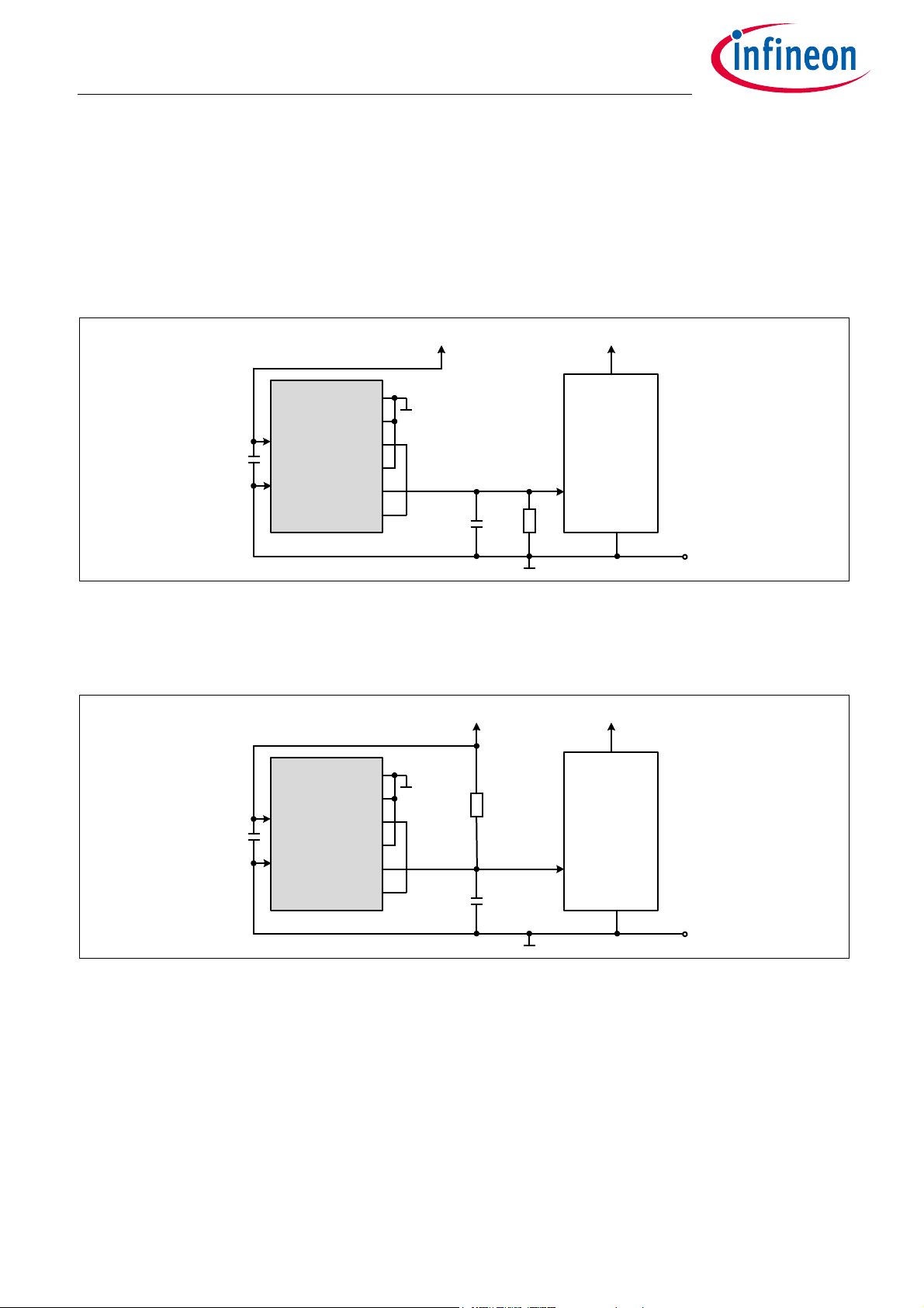
1 Application Circuits
The application circuits in this chapter show the various communication possibilities of the TLE5014.
Figure 1 shows a basic application circuit of a TLE5014 with PWM interface. The pull-down resistor is required
to ensure that the sensor starts with a low level after power-on or reset (PWM starts with a rising edge). If the
sensor is configured in such a way, that the PWM starts with a falling edge, the pull-down has to be replaced
by a pull-up.
Figure 1 Application circuit for TLE5014 with PWM, sensor configured to start with a rising edge of
PWM
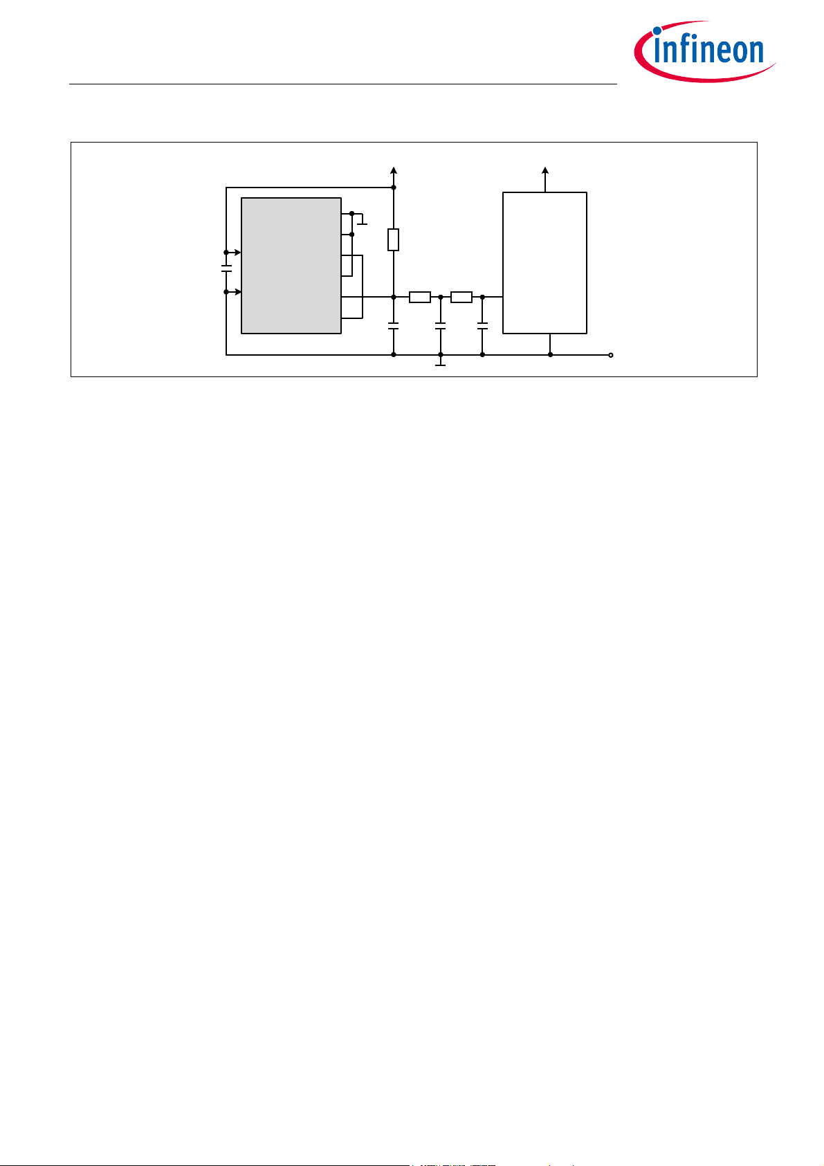
Figure 2 shows a basic application circuit of the TLE5014 with SPC mode.
Figure 2 Application circuit for TLE5014 with SPC, SPC address is configured to be “0” (IF1 and IF2
connected to GND)
The circuit shows the minimum external circuit which is needed to operate the SPC interface. The generation
of the trigger pulse (switch to pull the line low) is not shown. Depending on EMC requirements, additional
circuitry may be required. The value of C
and Rp are specified in the datasheet.
w
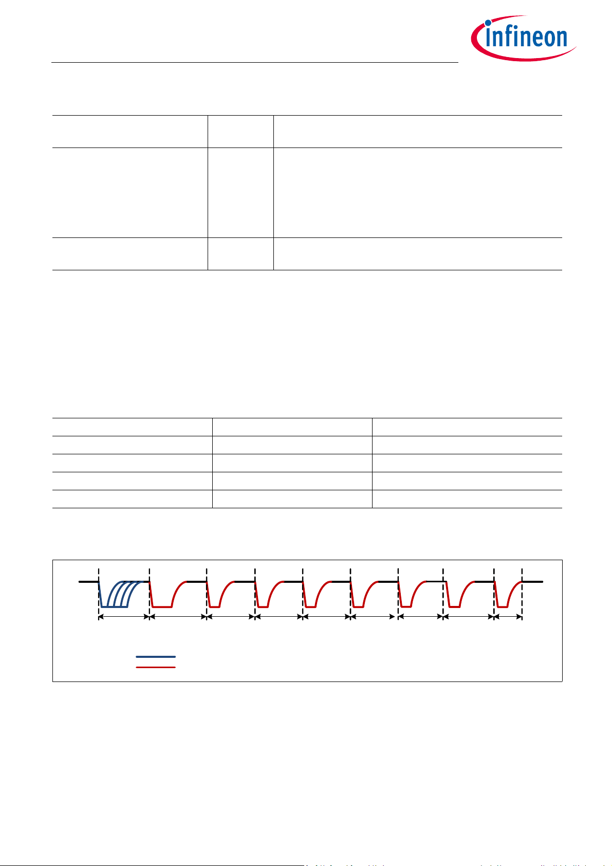
The TLE5014 can also be used with a SENT interface (Figure 3). The circuit shown is according to the SAE
J2716-2010 SENT specification.
User’s Manual 4 Rev. 1.0
2019-03-12
Page 5
TLE5014
TLE5014
GND
µControlle r
Master
10 0nF
V
DD
V
DD
GND
IF1
IF2
IF3
IFA
IFB
IFC
V
µC
10 k
56 0
10k
68 p 2 .2n 10 0p
GMR-Based Angle Sensor
Application Circuits
Figure 3 Application circuit for TLE5014 with SENT
User’s Manual 5 Rev. 1.0
2019-03-12
Page 6

TLE5014
GMR-Based Angle Sensor
Interfaces overview
2 Interfaces overview
Depending on the application, the TLE5014 is available with different interfaces:
• PWM (Pulse Width Modulation)
• SPC (Short PWM Code)
• SENT (Single Edge Nibble Transmission)
• SICI (Single-wire Interface for Calibration and Inspection; for programming purpose only)
PWM
The PWM is an unidirectional interface. Only one line is needed in which the angle value is transmitted. The
angle value corresponds to the duty cycle of the signal data. A reserved duty cycle range is implemented which
is used for indication of internal detected device errors. The data duty cycle range and the error duty cycle
range can be programmed via EEPROM setting.
SPC
The SPC is an interface based on the SENT protocol. The ECU (master µC) sends a trigger pulse which triggers
the TLE5014 to transmit the 12-bit angle value. If desired, the temperature can also be transmitted on a slow
channel (short serial message). The SPC also sends a CRC nibble and an end-pulse to terminate the
communication. One line is needed for the transmission and the pins IF1, IF2 and IFC are used to set the slave
number. Up to four slaves can be connected to one ECU; the ECU trigger pulse length will trigger the respective
sensor.
SENT
SENT is a standardized interface described in SAE J2716-2010.
SICI
A PWM based, bidirectional interface which is used for programming purpose only.
Further details on the SENT, SPC and PWM interface can be found in the data sheet of TLE5014.
2.1 PWM Interface Configuration
The following configuration of the PWM interface is possible. Further details are in the EEPROM register
description in Chapter 4.
Table 2 PWM Interface configuration
Parameter EEPROM
Register
PWM data duty cycle range
minimum value
PWM data duty cycle range
maximum value
PWM diagnostic duty cycle low 0x0064 This value determines the duty cycle which indicates a
User’s Manual 6 Rev. 1.0
0x0060 This value determines the low value of the duty cycle for
0x0062 This value determines the high value of the duty cycle for
Description
angle transmission. It corresponds to an angle value of 0°
angle transmission. It corresponds to an angle value of
359.91°
sensor failure detected by the internal safety mechanism
2019-03-12
Page 7

TLE5014
GMR-Based Angle Sensor
Interfaces overview
Table 2 PWM Interface configuration (cont’d)
Parameter EEPROM
Description
Register
PWM diagnostic duty cycle high 0x0066 This value determines the duty cycle which indicates a
sensor reset or a sensor start-up error (BIST error)
PWM predevider for PWM period 0x0068 This value is used for PWM frequency adjustment according
to Equation (4.1)
PWM period 0x006A This value is used for PWM frequency adjustment according
to Equation (4.1)
PWM starting edge 0x00A2 This value determines the starting edge of the PWM protocol.
It can be rising or falling. In case a rising edge is selected, the
PWM protocol will start with a HIGH level. In case a falling
edge is selected, it will start with a LOW
Care has to be taken when programming the low and high diagnostic duty cycle that there is no overlap with
the programmed data duty cycle range. In such a case, diagnostic information (e.g. sensor failure) could not
be distinguished from a valid transmitted angle value. It is recommended to add a safety margin between the
diagnostic and the data duty cycle range.
2.2 SPC Interface Configuration
The following table shows the different options for SPC interface configuration. The details for the EEPROM
setting are shown in Chapter 4.3
Table 3 SPC Interface configuration
Parameter EEPROM
Description
Register
SPC low time 0x00A2 This value can be 5 UT or 3UT. With 5UT, the SPC nibble is
compliant to the SENT specification
Temperature information in SPC
protocol
0x00A2 The SPC frame can contain two additional nibbles for
transmitting the temperature information
Rolling counter 0x00A2 A 4-bit rolling counter (rolling counter nibble) can be
activated which counts the transmitted frames. This is
necessary for functional safety applications to increase the
diagnostic coverage
Rolling counter in CRC 0x00A2 The rolling counter information can be coded in the CRC of
the SPC frame instead of being transmitted as extra nibble.
In this case the rolling counter information has 2 bit only.
This feature reduces overall frame length of the SPC protocol
SPC trigger 0x00A2 Two options are available for the total trigger length. It can
be constant with a length of 90 UT or variable. The variable
trigger length is t
time t
. Both settings can be used in a bus configuration as
low
the address of the sensor is defined by the low time t
+12 UT and depends on the trigger low
low
low
only.
The advantage of the variable trigger length is that the total
frame length can be reduced
User’s Manual 7 Rev. 1.0
2019-03-12
Page 8
TLE5014
Synchronisation
Frame
Trigger Nibble
µC Acti vity
Sensor Activity
90 UT
56 UT 12 … 27 UT 12 … 27 UT 12 … 27 UT 12 … 27 UT 12 … 27 UT 12 UT
Status Nibble
Data Nibble 1 Data Nibble 3Data Nibble 2 CRC
End
pulse
12 … 27 UT
Rolling counter
GMR-Based Angle Sensor
Interfaces overview
Table 3 SPC Interface configuration (cont’d)
Parameter EEPROM
Description
Register
SPC short serial message 0x00A2 A short serial message (slow message) can be activated,
which transmits one bit of a 16 bit information in each SPC
frame and thus needs 16 SPC frames for the whole data
transmission.This transmitted information is the
programmed angle base and rotation direction, the chip
temperature and 32 bit of the customer ID.
SPC unit time (UT) 0x00A2 The SPC unit time (UT) can be selected in the range of 1.0 µs
to 3.0 us.
SPC address setting in bus mode
The address of the sensor, so that it responds to a corresponding SPC trigger pulse, has to be set in the
EEPROM. All parts delivered from Infineon have the default address of ID = 0 in the EEPROM. Please refer to
description of EEPROM register 0x00A4 in Description EEPROM Address 0x00A4 CRC_CFG for correct setting.
The address of the sensor written to the EEPROM must be identical to the address of the sensor defined via
hard-wiring of the pins IF1, IF2 and IFC. Table 4 shows how the sensor address has to be set using the pins IF1,
IF2, IFC.
Table 4 SPC Address Configuration
Address IF1 IF2
0GNDGND
1IFCGND
2GNDIFC
3IFCIFC
Figure 4 shows a SPC frame with constant trigger length of 90UT, a status nibble, 3 data nibbles, a rolling
counter nibble and a CRC nibble. The low time of the trigger nibble determines the address of the sensor.
Figure 4 SPC frame with constant trigger length and rolling counter enabled as additional nibble
User’s Manual 8 Rev. 1.0
2019-03-12
Page 9

TLE5014
GMR-Based Angle Sensor
Interfaces overview
SPC status nibble
The 4-bit status nibble of the SPC protocol has different content depending on SPC protocol configuration:
• No short serial message:
Table 5 SPC Status Nibble
Bit Description
0 (LSB) Sensor ID (LSB)
1Sensor ID (MSB)
2 Internal sensor failure
3 (MSB) Sensor reset or start-up (BIST) failure
• Short serial message (SSM) enabled:
Table 6 SPC Status Nibble
Bit Description
0 (LSB) Data bit of SSM
1 Start bit of SSM
2 Internal sensor failure
3 (MSB) Sensor reset or start-up (BIST) failure
In this configuration, the sensor ID is coded in the CRC and not available in the status nibble. There is also the
option, that the rolling counter is not a dedicated nibble but the information is also coded in the CRC.
Therefore, four different versions of the CRC calculation exist:
• No short serial message (SSM) and rolling counter as nibble
Input data for the CRC calculation are:
STATUS & DATA1 & DATA2 & DATA3 & ROLLING_CNT
• Short serial message (SSM) enabled and rolling counter as nibble
the CRC calculation has to include a special 4-bit “ID-nibble” and is performed with the following input
data:
STATUS & DATA1 & DATA2 & DATA3 & ROLLING_CNT & ID_NIBBLE
ID_NIBBLE = (0 0 ID(MSB) ID(LSB))
• Short serial message (SSM) is disabled and rolling counter is included in CRC (no rolling counter as nibble)
The CRC calculation has to include a special 4-bit “RC-nibble” and is performed with the following input
data:
STATUS & DATA1 & DATA2 & DATA3 & RC_NIBBLE
RC_NIBBLE = (RC(MSB) RC(LSB) 0 0)
• Short serial message (SSM) is enabled and rolling counter is included in CRC (no rolling counter as nibble)
The CRC calculation has to include a special 4-bit “RC_ID-nibble” and is performed with the following input
data:
STATUS & DATA1 & DATA2 & DATA3 & RC_ID_NIBBLE
RC_ID_NIBBLE = (RC(MSB) RC(LSB) ID(MSB) ID(LSB))
User’s Manual 9 Rev. 1.0
2019-03-12
Page 10

TLE5014
GMR-Based Angle Sensor
Interfaces overview
Table 7 Examples for ID Nibble, RC_Nibble and ID_RC_Nibble calculation
ID RC ID_Nibble RC_Nibble RC_ID_Nibble
00
B
01
B
10
B
11
B
–00
–01
–10
–11
00
B
01
B
10
B
11
B
– 0000
– 0001
– 0010
– 0011
–0000B–
–0100B–
–1000–
–1100B–
– – 0000
– – 0101
– – 1010
– – 1111
00
01
10
11
B
B
B
B
B
B
B
B
B
B
B
B
––
––
––
––
B
B
B
B
Synchronization of the Rolling Counter
The first transmitted SPC frame has a rolling counter value of 0. The next frame transmits a rolling counter
value which is incremented by 1. In case the rolling counter is coded in the CRC, it is a 2-bit value. In this
configuration, a synchronization of the counter value (sensor value and counter value in the micro controller)
is required. The following two options are possible:
• Calculate the CRC with the received sensor data and a RC_NIBBLE of RC_NIBBLE = 0000
. Repeat this until
B
the calculated CRC matches with the transmitted CRC. This frame has the rolling counter value of 0. The
next transmitted frame has the incremented counter value of 1 and so on. As the rolling counter has 2 bit
in case it is coded in the CRC, latest the fourth transmitted frame needs to have a matched CRC. If this is
not the case an error occurred.
• For the first transmitted frame, calculate the four possible CRCs with the RC_NIBBLE values 0000
to 0011B.
B
The CRC which is matching the transmitted CRC has the correct rolling counter value. Use this value as
starting value which is incremented with the next received frame.
CRC calculation for SPC protocol
The checksum nibble is a 4-bit CRC of the data nibbles including the status nibble. The CRC is calculated using
a polynomial x4+x3+x2+1 with a seed value of 0101
. The remainder after the last data nibble is transmitted as
B
CRC. The CRC calculation method is based on “recommended” implementation in the SENT standard 2010.
For this “recommended” implementation, the CRC is calculated based on the input data which is then
augmented with four extra zero bits and an additional CRC calculation step.
Code example:
//Table CRC, Poly=0xD
uint8_t cr4Table[16] = {0, 13, 7, 10, 14, 3, 9, 4, 1, 12, 6, 11, 15, 2, 8, 5};
//Example:
//Status Nibble = 0x6
//Data Nibble = 0x7, 0x4, 0x8, 0x7, 0x4, 0x8
uint8_t nibble[7] = {6, 7, 4, 8, 7, 4, 8};
uint8_t nb_nibble = 0x7;
User’s Manual 10 Rev. 1.0
2019-03-12
Page 11

TLE5014
GMR-Based Angle Sensor
Interfaces overview
//Seed value = 0x5
uint8_t crc = 0x5;
for(uint8_t i=0;i<nb_nibble;i++){
crc = nibble[i] ^ cr4Table[crc];
}
//Final XOR
crc = 0x0 ^ cr4Table[crc];
2.3 SENT Interface Configuration
The following table shows the different options for SENT interface configuration.
Table 8 SENT Interface configuration
Parameter EEPROM
Register
SENT low time 0x00A2 This value can be 5 UT or 3 UT. With 5 UT, the nibble is
SENT protocol type 0x00A2 Two different SENT implementations can be configured:
Sent short serial message 0x00A2 A short serial message (slow message) can be activated
SENT error indication 0x00A2 In case of an internal chip error, the error can be indicated
Se nt u nit time (UT) 0x 00A 2 The SE NT uni t tim e (UT ) can be sel ecte d in th e ran ge of 1.5 µ s
Description
compliant to the SENT specification
Standard SENT: Status nibble, 3 x 4-bit data nibbles, CRC
nibble
Single Secure SENT: Status nibble, 3 x 4-bit data nibbles, 2x4bit rolling counter; Inverted data nibble, CRC nibble
which transmits one bit of additional information in each
SPC frame. This transmitted information is the programmed
angle base and rotation direction, the chip temperature and
32 bit of the customer ID
only in the status nibble by setting an error bit or in the status
nibble and also in the SENT data range. In this case an error
code of “4091” is sent. For this option, the data range has not
the full 12-bit resolution but only 1 … 4088 LSB
to 3.0 us
SENT Status Nibble
The 4-bit status nibble of the SENT protocol contains the following information:
Table 9 SENT Status Nibble
Bit Description
0 (LSB) error indication or start-up (BIST) error or sensor reset
1 reserved
2 short serial message bit (data bit)
3 (MSB) short serial message bit (start indication)
User’s Manual 11 Rev. 1.0
2019-03-12
Page 12

TLE5014
GMR-Based Angle Sensor
Interfaces overview
CRC calculation for SENT protocol
The checksum nibble is a 4-bit CRC of the data nibbles and does not include the status nibble (different to SPC
CRC implementation). The CRC is calculated using a polynomial x4+x3+x2+1 with a seed value of 0101
remainder after the last data nibble is transmitted as CRC. The CRC calculation method is based on
“recommended” implementation in the SENT standard 2010. For this “recommended” implementation, the
CRC is calculated based on the input data (without STATUS nibble) which is then augmented with four extra
zero bits and an additional CRC calculation step.
Code example:
//Table CRC, Poly=0xD
uint8_t cr4Table[16] = {0, 13, 7, 10, 14, 3, 9, 4, 1, 12, 6, 11, 15, 2, 8, 5};
//Example:
//Data Nibble = 0x7, 0x4, 0x8, 0x7, 0x4, 0x8
uint8_t nibble[6] = {7, 4, 8, 7, 4, 8};
uint8_t nb_nibble = 0x6;
//Seed value = 0x5
uint8_t crc = 0x5;
. The
B
for(uint8_t i=0;i<nb_nibble;i++){
crc = nibble[i] ^ cr4Table[crc];
}
//Final XOR
crc = 0x0 ^ cr4Table[crc];
User’s Manual 12 Rev. 1.0
2019-03-12
Page 13

TLE5014
GMR-Based Angle Sensor
EEPROM Page Map
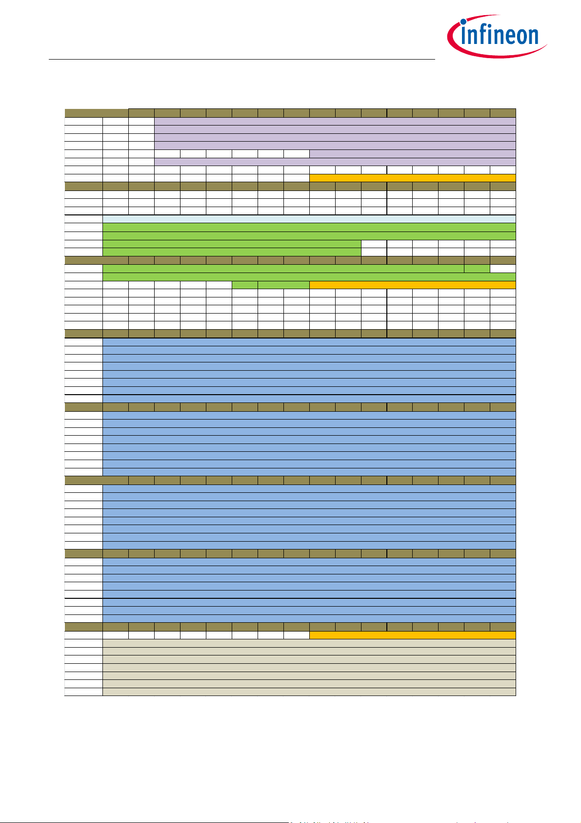
3 EEPROM Page Map
The TLE5014 has an EEPROM as non-volatile memory where sensor configuration data can be stored. The
memory is organized in pages, each page contains 8 registers, each register has 16 bit. Some pages and
registers can be accessed by the user and the content can be modified thus changing chip configuration. Care
has to be taken when modifying content of the EEPROM as the device behavior can be changed and no or
wrong output data can be generated. There is no automatic restore functionality where the pre-programmed
status can be recovered.
The EEPROM content is secured by a CRC. In case any content of the EEPROM is changed, the CRC has to be
recalculated and written to the corresponding register, otherwise an error is indicated. The CRC has always be
calculated out of several pages and registers, which are indicated in the description of the corresponding CRC
(Table 10). The algorithm for the CRC calculation is described in Chapter 6.2.3.
The following Table 10 shows the pages and EEPROM registers of each page and their function. A detailed
description of the EEPROM registers and the possible settings can be found in Chapter 4.
The startup value of each configuration register of the TLE5014 is stored in a corresponding EEPROM register,
which can be modified by the user. Table 10 lists the allocation of the user-configurable EEPROM pages.
Care shall be taken when the EEPROM configuration is changed, as not all possible configurations are released
by Infineon. This means, that they can be used for testing purpose but not necessarily for production. All
released configurations can be found in the TLE5014 datasheet.
Table 10 EEPROM page map
Page EEPROM
Register
0x006 0x0060 OUT_LIM_MIN PWM data duty cycle range minimum
0x0062 OUT_LIM_MAX PWM data duty cycle range maximum
0x0064 OUT_STAT_L PWM diagnostic duty cycle low
0x0066 OUT_STAT_H PWM diagnostic duty cycle high
0x0068 TMR_PREDIV PWM predevider for PWM period
0x006A TMR_PERIOD PWM period
0x006C – Reserved
0x006E CRC_EEP CRC has to be calculated with following
Name Description Default value of Reg.
value
value
values: page 0x002 & 0x003 & 0x004 &
0x005 & register 0x0060 & 0x0062 &
0x0064 & 0x0066 & 0x0068 & 0x006A &
0x006C & first byte of 0x006E (bit [15:8] &
0xFF00)
User’s Manual 13 Rev. 1.0
2019-03-12
Page 14

TLE5014
GMR-Based Angle Sensor
EEPROM Page Map
Table 10 EEPROM page map (cont’d)
Page EEPROM
Register
0x009 0x0090 – Reserved
0x0092 – Reserved
0x0094 – Reserved
0x0096 ACSTAT Activation of internal safety mechanism
0x0098 MOD1 3 V/5 V, pad configuration, LUT options
0x009A MOD2 Lock function for register PWI_MD_USR
0x009C IF123_CFG Pin configuration of pin IF1, IF2, IF3
0x009E IFABC_CFG Pin configuration of pin IFA, IFB, IFC
0x00A 0x00A0 ANG_BASE Angle base & rotation direction
0x00A2 PWI_MD_USR Interface configuration
0x00A4 CRC_CFG Configuration CRC and SPC address;
Name Description Default value of Reg.
CRC has to be calculated with following
values: registers 0x0096 & 0x0098 &
0x009A & 0x009C & 0x009E & 0x00A0 &
0x00A2 & first byte of 0x00A4 (bit [15:8] &
0xFF00)
0x00A6 – Reserved
0x00A8 – Reserved
0x00AA – Reserved
0x0AC – Reserved
0x00AE – Reserved
0x00B 0x00B0 LUT_0 Look-up table value for 0°
0x00B2 LUT_1 Look-up table value for 11.25°
0x00B4 LUT_2 Look-up table value for 22.50°
0x00B6 LUT_3 Look-up table value for 33.75°
0x00B8 LUT_4 Look-up table value for 45.00°
0x00BA LUT_5 Look-up table value for 56.25°
0x00BC LUT_6 Look-up table value for 67.50°
0x00BE LUT_7 Look-up table value for 78.75°
0x00C 0x00C0 LUT_8 Look-up table value for 90.00°
0x00C2 LUT_9 Look-up table value for 101.25°
0x00C4 LUT_10 Look-up table value for 112.50°
0x00C6 LUT_11 Look-up table value for 123.75°
0x00C8 LUT_12 Look-up table value for 135.00°
0x00CA LUT_13 Look-up table value for 146.25°
0x00CC LUT_14 Look-up table value for 157.50°
0x00CE LUT_15 Look-up table value for 168.75°
User’s Manual 14 Rev. 1.0
2019-03-12
Page 15

TLE5014
GMR-Based Angle Sensor
EEPROM Page Map
Table 10 EEPROM page map (cont’d)
Page EEPROM
Register
0x00D 0x00D0 LUT_16 Look-up table value for 180.00°
0x00D2 LUT_17 Look-up table value for 191.25°
0x00D4 LUT_18 Look-up table value for 202.50°
0x00D6 LUT_19 Look-up table value for 213.75°
0x00D8 LUT_20 Look-up table value for 225.00°
0x00DA LUT_21 Look-up table value for 236.25°
0x00DC LUT_22 Look-up table value for 247.50°
0x00DE LUT_23 Look-up table value for 258.75°
0x00E 0x00E0 LUT_24 Look-up table value for 270.00°
0x00E2 LUT_25 Look-up table value for 281.25°
0x00E4 LUT_26 Look-up table value for 292.50°
0x00E6 LUT_27 Look-up table value for 303.75°
0x00E8 LUT_28 Look-up table value for 315.00°
0x00EA LUT_29 Look-up table value for 326.25°
0x00EC LUT_30 Look-up table value for 337.50°
Name Description Default value of Reg.
0x00EE LUT_31 Look-up table value for 348.75°
0x00F 0x00F0 [7:0] CRC_LUT 8-bit CRC for Look-up table; CRC has to
be calculated with following values:
page 0x00B & 0x00C & 0x00D & 0x00E &
first byte of register 0x00F0 (bits [15:8] &
0xFF00)
0x00F2 CUST_ID_0 16-bit of customer ID, will be
transmitted via short serial message
0x00F4 CUST_ID_1 16-bit of customer ID, will be
transmitted via short serial message
0x00F6 CUST_ID_2 16-bit of customer ID
0x00F8 CUST_ID_3 16-bit of customer ID
0x00FA CUST_ID_4 16-bit of customer ID
0x00FC CUST_ID_5 16-bit of customer ID
0x00FE CUST_ID_6 16-bit of customer ID
User’s Manual 15 Rev. 1.0
2019-03-12
Page 16
TLE5014
Page 0x006 1514131211109876543210
0x0060 - -
0x0062 - -
0x0064 - -
0x0066 - -
0x0068 - - ------
0x006A - -
0x006C - - -------------
0x006E - - ------
Page 0x009
0x0090 - - --------------
0x0092 - - --------------
0x0094 - - --------------
0x0096
0x0098
0x009A
0x009C ------
0x009E ------
Page 0x00A
0x00A0 ANG_DIR -
0x00A2
0x00A4 -----AS_NR
0x00A6 - - --------------
0x00A8 - - --------------
0x00AA - - --------------
0x00AC - - --------------
0x00AE - - --------------
Page 0x00B
0x00B0
0x00B2
0x00B4
0x00B6
0x00B8
0x00BA
0x00BC
0x00BE
Page 0x00C
0x00C0
0x00C2
0x00C4
0x00C6
0x00C8
0x00CA
0x00CC
0x00CE
Page 0x00D
0x00D0
0x00D2
0x00D4
0x00D6
0x00D8
0x00DA
0x00DC
0x00DE
Page 0x00E
0x00E0
0x00E2
0x00E4
0x00E6
0x00E8
0x00EA
0x00EC
0x00EE
Page 0x00F
0x00F0 --------
0x00F2
0x00F4
0x00F6
0x00F8
0x00FA
0x00FC
0x00FE
CUST_ID_2
CUST_ID_3
CUST_ID_4
CUST_ID_5
CUST_ID_6
CUST_ID_0
CUST_ID_1
LUT_22
LUT_23
LUT_24
LUT_25
LUT_26
LUT_27
CRC_LUT
LUT_28
LUT_29
LUT_30
LUT_31
LUT_21
LUT_10
LUT_11
LUT_12
LUT_13
LUT_14
LUT_15
LUT_16
LUT_17
LUT_18
LUT_19
LUT_20
LUT_8
LUT_9
LUT_3
LUT_4
LUT_5
LUT_6
LUT_7
TMR_PERIOD
CRC_EEP
LUT_0
LUT_1
LUT_2
ANG_BASE
ACSTAT
MOD1
MOD2
IF123_CFG
IFABC_C FG
PWI_MOD
S_NR_EEP CRC_CFG
OUT_LIM_MIN
OUT_LIM_MAX
OUT_STAT_L
OUT_STAT_H
TMR_PREDIV
GMR-Based Angle Sensor
EEPROM Page Map
Figure 5 TLE5014 EEPROM bitmap
User’s Manual 16 Rev. 1.0
2019-03-12
Page 17

TLE5014
GMR-Based Angle Sensor
EEPROM Register Description
4 EEPROM Register Description
This chapter describes the EEPROM registers which can be accessed via SICI in the EEPROM programming
mode. Further registers needed for EEPROM programming are described in Chapter 7.1.
Care shall be taken that there is no unintended modification of bits. When modifying registers, reserved bits
have to be read and written back with the same value.
4.1 Page 0x006
The page 0x06 is used for the configuration of the PWM protocol. It is only relevant in case PWM is selected as
interface in the register PWI_MD_USR (0x00A2). The following tables EEPROM Register Address 0x0060
OUT_LIM_MIN to EEPROM Register Address 0x006E CRC_EEP show the details.
EEPROM Register Address 0x0060 OUT_LIM_MIN
1514131211109876543210
OUT_LIM_MIN
Field Bits Type Description
OUT_LIM_MIN 13:0
Minimum value of data duty cycle range; 0% … 100% mapped to
0 … 16383
EEPROM Register Address 0x0062 OUT_LIM_MAX
1514131211109876543210
OUT_LIM_MAX
Field Bits Type Description
OUT_LIM_MAX 13:0
Maximum value of data duty cycle range; 0% … 100% mapped to
0 … 16383
EEPROM Register Address 0x0064 OUT_STAT_L
1514131211109876543210
OUT_STAT_L
User’s Manual 17 Rev. 1.0
2019-03-12
Page 18

TLE5014
GMR-Based Angle Sensor
EEPROM Register Description
Field Bits Type Description
OUT_STAT_L 13:0
Low value of diagnostic duty cycle; 0% … 100% mapped to 0 … 16383
EEPROM Register Address 0x0066 OUT_STAT_H
1514131211109876543210
OUT_STAT_H
Field Bits Type Description
OUT_STAT_H 13:0
High value of diagnostic duty cycle; 0% … 100% mapped to 0 … 16383
EEPROM Register Address 0x0068 TMR_PREDIV
1514131211109876543210
TMR_PREDIV
Field Bits Type Description
TMR_PREDIV 7:0
For calculation of PWM frequency according to Equation (4.1)
EEPROM Register Address 0x006A TMR_PERIOD
1514131211109876543210
TMR_PERIOD
Field Bits Type Description
TMR_PERIOD 13:0
For calculation of PWM frequency according to Equation (4.1)
EEPROM Register Address 0x006E CRC_EEP
1514131211109876543210
CRC_EEP
User’s Manual 18 Rev. 1.0
2019-03-12
Page 19

TLE5014
fHz[]
40000000
1 TMR_PREDIV+()TMR_PERIOD()
----------------------------------------------------------------------------------------------
=
GMR-Based Angle Sensor
EEPROM Register Description
Field Bits Type Description
CRC_EEP 7:0
CRC has to be calculated with following values: page 0x002 & 0x003 &
0x004 & 0x005 & register 0x0060 & 0x0062 & 0x0064 & 0x0066 & 0x0068
& 0x006A & 0x006C & first byte of 0x006E (bit [15:8])
The PWM frequency of the PWM output can be programmed with the two parameters TMR_PREDIV and
TMR_PERIOD according to the following Equation (4.1):
(4.1)
Example:
For TMR_PREDIV = 12, TMR_Period = 15384, the PWM frequency calculates to f = 200 Hz.
4.2 Page 0x009
Care has be taken that there is no unintended modification of bits. When modifying registers, reserved bits
have to be read and written back with the same value.
Description EEPROM Register Address 0x0098 MOD1
1514131211109876543210
RST_3_5CLK_SELFIR_M
D
LUT_MD IFMD_ABC
Field Bits Type Description
RST_3_5 13
0:
Reset comparator set to < 3.0 V
B
1:
Reset comparator set to < 4.2 V
B
CLK_SEL 12
For test purpose only
IFMD_
123
FIR_MD 11
Internal update rate of angle calculation:
0:
25.6 µs
B
51.2 µs
1:
B
LUT_MD 9:8
Look-up table (LUT) configuration:
LUT disabled
00:
B
01:
LUT range = 360° (angle steps = 11.25°)
B
LUT range = 180° (angle steps = 5.625°)
10:
B
11:
LUT range = 90° (angle steps = 2.813°)
B
User’s Manual 19 Rev. 1.0
2019-03-12
Page 20

TLE5014
GMR-Based Angle Sensor
EEPROM Register Description
Field Bits Type Description
IFMD_ABC 5:4
For test purpose only
IFMD_123 0
For test purpose only
Description EEPROM Register Address 0x009A MOD2
1514131211109876543210
MOD2
Field Bits Type Description
MOD2 15:0
Lock register for 0x00A2. The bits in this registers are connected with a
logical AND function with the corresponding bit in 0x00A2. This means
that a “0” in a bit of register 0x009A prohibits to set a “1” in the
corresponding bit of 0x00A2. Note: The bit will show as “1” in 0x00A2
but has no effect
Description EEPROM Register Address 0x009C IF123_CFG
1514131211109876543210
PAD_
OV_O
FF
PAD_S
PIKE
IF3_ODIF3_CFGIF2_ODIF2_CFGIF1_ODIF1_C
FG
Field Bits Type Description
PAD_OV_OFF 15
Enable/disable overvoltage functionality. Output deactivated in case
of overvoltage on V
Overvoltage functionality enabled
0:
B
1:
Overvoltage functionality disabled
B
DD
:
PAD_SPIKE 14
Activate spike filter for input stage:
0:
Spike filter disabled
B
Spike filter enabled
1:
B
IF3_OD 11
IF3 open drain enable:
Disable (Push-Pull)
0:
B
1:
Enable (Open Drain)
B
User’s Manual 20 Rev. 1.0
2019-03-12
Page 21

TLE5014
GMR-Based Angle Sensor
EEPROM Register Description
Field Bits Type Description
IF3_CFG 10
For test purpose only
IF2_OD 9
IF2 open drain enable:
0:
Disable (Push-Pull)
B
Enable (Open Drain)
1:
B
IF2_CFG 8
For test purpose only
IF1_OD 7
IF1 open drain enable:
Disable (Push-Pull)
0:
B
1:
Enable (Open Drain)
B
IF1_CFG 6
For test purpose only
Description EEPROM Register Address 0x009E IFABC_CFG
1514131211109876543210
IFB_SLP
IFC_ODIFC_CFGIFB_ODIFB_CFGIFA_ODIFA_C
FG
Field Bits Type Description
IFB_SLP 15:14
Slope control of output signal:
00:
2µs
B
01:
4µs
B
10:
6µs
B
Tristate
11:
B
IFC_OD 11
IFC open drain enable:
Disable (Push-Pull)
0:
B
1:
Enable (Open Drain)
B
IFC_CFG 10
For test purpose only
IFB_OD 9
IFB open drain enable:
0:
Disable (Push-Pull)
B
1:
Enable (Open Drain with edges control)
B
IFB_CFG 8
For test purpose only
User’s Manual 21 Rev. 1.0
2019-03-12
Page 22

TLE5014
GMR-Based Angle Sensor
EEPROM Register Description
Field Bits Type Description
IFA_OD 7
IFA open drain enable:
0:
Disable (Push-Pull)
B
Enable (Open Drain)
1:
B
IFA_CFG 6
For test purpose only
4.3 Page 0x00A
Care has be taken that there is no unintended modification of bits. When modifying registers, reserved bits
have to be read and written back with the same value.
Description EEPROM Address 0x00A0 ANG_BASE
1514131211109876543210
ANG_BASE
Field Bits Type Description
ANG_BASE 15:2
Signed 14 bit value:
0° = 0x0000
-180.000° = 0x2000
+179.978° = 0x1FFF
+0.02197° = 0x001
ANG_DIR 1
Direction of magnet rotation:
0:
ccw
B
1:
cw
B
Reserved 0
0:
Reserved bit, shall not be changed
B
Description EEPROM Address 0x00A2 PWI_MD_USR
ANG_
DIR
Reser
ved
1514131211109876543210
EDGE
SENT/
SPC_L
T_5_3
SPC_T
EMP
SPC_R
CNIB
SPC_R
CCRC
SPC_T
PWI_MODE
User’s Manual 22 Rev. 1.0
PWM_
RIG
SENT_
PROM
O
SENT_
ERR_S
IG
SENT_
PAPU
SENT/
SPC_P
WI_SS
M
SENT/SPC_UT
2019-03-12
Page 23

TLE5014
GMR-Based Angle Sensor
EEPROM Register Description
Field Bits Type Description
PWI_MODE 15:13
Interface selection (Only available for Product Type: TLE5014F16D):
100:
PWM
B
SENT
010:
B
001:
SPC
B
PWM _EDGE 12
PWM starting edge:
0:
Rising edge
B
Falling edge
1:
B
SENT/SPC_LT_
5_3
SPC_TEMP 10
SPC_RCNIB 9
SPC_RCCRC 8
SPC_TRIG 7
SENT_PROMO 6
11
SENT/SPC low time:
5UT
0:
B
1:
3UT
B
Temperature information in SPC protocol:
0:
No temperature nibble
B
1:
Two temperature nibbles
B
Rolling counter:
0:
Rolling counter nibble enabled
B
No rolling counter nibble
1:
B
Rolling counter in CRC:
No rolling counter in CRC
0:
B
1:
Rolling counter in CRC
B
SPC bus mode:
0:
90 UT constant trigger length
B
1:
Variable trigger length
B
SENT protocol type:
0:
Single secure sensor (with rolling counter and inverted data
B
nibble)
1:
Standard SENT (without rolling counter and inverted data
B
nibble)
SENT_ERR_SIG 5
SENT error indication:
Error code “4091” in data range
0:
B
1:
Error indication in status nibble only
B
SENT_PAPU 4
Pause pulse activation:
0:
No pause pulse
B
1:
Pause pulse activated
B
User’s Manual 23 Rev. 1.0
2019-03-12
Page 24

TLE5014
GMR-Based Angle Sensor
EEPROM Register Description
Field Bits Type Description
SENT/SPC_PWI
_SSM
3
SENT/SPC short serial message:
0:
No short serial message
B
Short serial message activated
1:
B
SENT/SPC_UT 2:0
SENT/SPC unit time setting:
3µs
000:
B
001:
2.5 µs
B
2.0 µs
010:
B
011:
1.5 µs
B
100:
1.0 µs
B
Description EEPROM Address 0x00A4 CRC_CFG
1514131211109876543210
AS_N
S_NR_EEP CRC_CFG
R
Field Bits Type Description
AS_NR 10
0:
Address configuration for SICI as defined in bits S_NR_EEP
B
Address configuration for SICI as defined by hard wiring of pins
1:
B
Note: This bit shall be set to “1”, otherwise no programming in bus
S_NR_EEP 9:8
Address coding of SPC slave:
00:
ID = 0
B
01:
ID = 1
B
ID = 2
10:
B
11:
ID = 3
B
CRC_CFG 7:0
Configuration CRC and SPC address; CRC has to be calculated with
following values: registers 0x0096 & 0x0098 & 0x009A & 0x009C &
0x009E & 0x00A0 & 0x00A2 & first byte of 0x00A4 (bit [15:8])
4.4 Page 0x00B - 0x00E
Look-up table, see Table 10.
mode is possible. SPC protocol is always using the values
from bits S_NR_EEP
4.5 Page 0x00F
In EEPROM register 0x00F0 the 8-bit CRC for the look-up table is stored.
User’s Manual 24 Rev. 1.0
2019-03-12
Page 25

TLE5014
GMR-Based Angle Sensor
EEPROM Register Description
Description EEPROM Address 0x00F0 CRC_LUT
1514131211109876543210
CRC_LUT
Field Bits Type Description
CRC_LUT 7:0
8-bit CRC has to be calculated with following values:
Page 0x00B & 0x00C & 0x00D & 0x00E & first byte of 0x00F0 (bits [15:8])
In the EEPROM registers 0x00F2 to 0x00FE the customer ID is stored. In total it is 16 x 7 = 112 bit.
The first 32 bits (EEPROM address 0x00F2 and 0x00F4) are transmitted in the short serial message.
User’s Manual 25 Rev. 1.0
2019-03-12
Page 26

TLE5014
GMR-Based Angle Sensor
Working Register Description
5 Working Register Description
This chapter describes the working registers which can be read with the SICI interface. These registers are
updated with the time t
5.1 STAT Register 0x00: Status
This register provides detailed information on sensor status and internal sensor errors.
Register Address 0x00: STAT (Status)
1514131211109876543210
, which is approximately 25 µs.
update
Read Command: 0xC001
RD_ST RES S_IF S_VEC RES RES S_EEP S_CRC
uuuu uuuuuuuuuu
S_PROGS_BISTS_ADC
T
S_ADC S_VR S_WD
S_PLA
USI
S_RST
Field Bits Type Description
RD_ST 15 u
Read bit that indicates that the bits in the STAT-line are updated since
the last readout
RES 14 u
Reserved
S_IF 13 u
Bit is set when a interface issue happened
S_VEC 12 u
Bit indicates when the vector length of the actual angle_vector
exceeds the defined limits
RES 11
Reserved
RES 10
Reserved
S_EEP 9u
Bit indicates whenever the EEPROM initiates an error
S_CRC 8u
Bit is set whenever one of the bit error detection functions is alarming
S_PROG 7u
Bit indicates a DSP error
S_BIST 6u
Bit is set whenever one of the startup-BIST is failing. (BIST: Built in self
test)
S_ADCT 5u
Bit is set when the temperature is out of limits or the temperature
delta check is failing
S_ADC 4u
Bit is set when the ADC_raw_max or ADC_raw_delta check fails or the
filter-scheduling check is alarming
User’s Manual 26 Rev. 1.0
2019-03-12
Page 27

TLE5014
GMR-Based Angle Sensor
Working Register Description
Field Bits Type Description
S_VR 3u
Bit is a combination of several voltage checks
S_WD 2u
Bit is set when the last reset happened due to a watchdog event
S_PLAUSI 1u
Bit is set when the redundant angle calculation is failing the limits
S_RST 0u
Reset occurred
5.2 AVAL Register 0x02: Angle Value
The current angle value can be read via SICI interface in register AVAL at address 0x02. It is updated approx.
every 25 µs, which is the time needed for sampling and calculating a new angle value. It is a signed 15-bit value
(see Description Register Address 0x02 AVAL).
Description Register Address 0x02 AVAL
Read command: 0x8021
1514131211109876543210
RD_AV AVAL
Field Bits Type Description
RD_AV 15
Read bit that indicates that the bits in the AVAL register are updated
since last readout by interface
AVAL 14:0
Signed 15-bit internal angle value:
0° = 0x0000
-180° = 0x4000
179.99° = 0x3FFF
5.3 ASPD Register 0x03: Angle Speed
This register provides the actual angle speed.
Register Address 0x03: Angle speed
Read command: 0xC031
1514131211109876543210
RD_AS
PD
uu
User’s Manual 27 Rev. 1.0
RES ASPD
2019-03-12
Page 28

TLE5014
speed ° s⁄[]
360°
65536
---------------
ASPD digits[]×
t
update s[]
----------------------------------------------------------
=
GMR-Based Angle Sensor
Working Register Description
Field Bits Type Description
RD_ASPD 15 u Read angle speed
Read bit that indicates that the bits in the ASPD-register are updated
since last readout by interface
RES 14:12
Reserved
ASPD 11:0 u Angle speed
Calculated angle speed signed 12-bit value
5.4 RAW_X Register 0x06: X raw value
This register provides the x-raw value (cosine value).
Register Address 0x06: X raw value
Read command: 0xC061
1514131211109876543210
RAW_X
u
Field Bits Type Description
RAW_X 15:0 u
Unsigned 16-bit value of X-raw
5.5 RAW_Y Register 0x07: Y raw value
This register provides the y-raw value (sine value).
Register Address 0x07: Y raw value
Read command: 0x8071
1514131211109876543210
RAW_Y
u
Field Bits Type Description
RAW_Y 15:0 u
Unsigned 16-bit value of Y-raw
User’s Manual 28 Rev. 1.0
2019-03-12
Page 29

TLE5014
GMR-Based Angle Sensor
Working Register Description
5.6 TEMP Register 0x0A: Temperature raw value
This register provides the actual raw temperature value. To calculate the actual temperature, the temperature
offset has to be determined. This is done by reading the register once at a known temperature (e.g. 25°C) This
value is then TEMPER_25 and the offset corrected temperature can be calculated using the formula below.
Register Address 0x0A: temperature raw value
Read command: 0xC0A1
1514131211109876543210
TEMP_VALUE
rrr
Field Bits Type Description
TEMP_VALUE 15:6 r Temperature value
10-bit temperature value, not offset corrected
T [°C] = (TEMP_VALUE-TEMPER_25) / 1.3815 [LSB/°C] + 25°C
TEMPER_25: TEMP_VALUE @25°C
In case the offset correction is not done at 25°C but at a different
temperature, the formula has to be modified accordingly.
RD_SM 5rRead state machine
Bit is set when new value is available since state machine has read
last one
RD_INT 4rRead interface
Bit is set when new value is available since interface has read last one
RES 3:0
Reserved
RD_SMRD_IN
T
RES
5.7 ANG_BASE register 0x14: Angle base and rotation direction
This register contains the angle base. The output angle is referring to this angle base value.
Register Address 0x14: angle base and rotation direction
Read command: 0xC141
1514131211109876543210
ANG_BASE
ww
User’s Manual 29 Rev. 1.0
ANG_
DIR
2019-03-12
RES
Page 30

TLE5014
GMR-Based Angle Sensor
Working Register Description
Field Bits Type Description
ANG_BASE 15:2 w Angle base
signed 14 bit zero angle value.
Output angle is referring to this angle base
0x0000 = 0°,
0x2000 = -180°,
0x1FFF = +179,978°,
0x001 = 0,02197°
ANG_DIR 1wDirection of the angle rotation
0 = clockwise
1 = counter clockwise
RES 0
Reserved
User’s Manual 30 Rev. 1.0
2019-03-12
Page 31

TLE5014
GMR-Based Angle Sensor
SICI
6SICI
6.1 Basic Functionality
The SICI interface (SICI: Single-Wire Interface for Calibration and Inspection) is a one-wire programming
interface that allows read and write access to the working registers and EEPROM registers of the sensor. It is
bidirectional for every transferred bit, meaning that for every single bit sent by the master one bit is
immediately sent back from the slave. The speed of the interface is automatically determined from the length
of the first bit sent by the master.
The one-wire interface enables a robust data transmission at a speed of up to 240 kbit/s. It is a voltage
interface based on a bit-wise pulse-width-modulation (PWM) principle and requires an open-drain driver on
micro controller side. Regardless of the interface configuration of the TLE5014, the SICI interface is always
available on the IFB pin during the startup time.
In order to use the SICI interface, sensor and micro controller have to use an open drain output, so they can
actively pull a “low” level. The communication line has to be connected to V
1.5-2 kΩ. Higher values for the pull-up resistor may lead to problems to achieve the necessary speed of the
communication.
by a pull-up resistor of approx.
DD
6.2 SICI Data Transfer
The communication via the SICI interface is based on transmitting a single bit to the sensor and immediately
receiving a bit. These bits form a 16-bit word. It makes the interface bit-synchronous, robust and very flexible
in timing. Bidirectional data transmission can thus be realized using only a single wire without a trimmed
oscillator on sensor or master side. To enhance the robustness of the interface, the sensor repeats the 16-bit
command word sent by the master in order to have a confirmation of the correct understanding of the
message, and transmits a safety word after each communication. Additionally, a time-out feature is
implemented: If during a communication the sensor does not receive a bit from the master within a certain
time span (see Table 11, Interface reset time), the interface is reset and a new command can be sent.
6.2.1 Bit Encoding
For the SICI interface, bits are encoded as the difference in duration of consecutive “low” and “high” levels. To
transmit a bit to the sensor, the master sends one single low/high PWM signal with a period T, then pulls the
line to “low” again for a short time T
“low” and “high” time:
• to transmit a “0” to the sensor, the master pulls the line “low” for a short time T
for a long time T - T
(typically T1=0.3*T)
1
• to transmit a “1” to the sensor, the master pulls the line “low” for a long time T
for a short time T - T
(typically T2=0.7*T)
2
The sensor recognizes the total bit-time interval T as the duration between two consecutive falling edges from
the master. This encoding scheme is illustrated in Figure 6.
. The logic value of the bit is then encoded as the difference between
3
, then releases it to “high”
1
, then releases it to “high”
2
User’s Manual 31 Rev. 1.0
2019-03-12
Page 32

TLE5014
T
0:
1:
T
1
T
2
ΔT = T – 2*T
1
ΔT = 2*T2-T
ΔT
master pulls low
line is released
0
1
GND
V
DD
T
3
1
0
Δ T
Master checks
resp onse here
Master pulls low
Sensor pulls low
Line is released
V
DD
GND
GMR-Based Angle Sensor
SICI
Figure 6 Timing description of master bit
After receiving a bit from the master, the sensor answers by transmitting one bit:
• the sensor transmits a “1” by pulling the SICI-line “low” for the time difference ∆T between “high” and
“low” level given by the received PWM signal (i.e. if a “0” was transmitted by the master, ∆T = T -2*T
whereas if a “1” was transmitted by the master, ∆T =2*T
• the sensor transmits a “0” by keeping the line “high”
To read the bit transmitted by the sensor, the master has to check the level of the line after T
pulse) but before time ∆T has expired (recommended 80% of ∆T, see Figure 7).
2
- T)
(master low
3
,
1
Figure 7 Timing description of response bit from sensor
After receiving the response bit from the sensor, the master can pause for a time T
next bit. T
interface is reset. Figure 8 shows an example communication between master and sensor.
User’s Manual 32 Rev. 1.0
has to be shorter than the time-out limit (see Table 11, interface reset time), otherwise the
4
before transmitting the
4
2019-03-12
Page 33

TLE5014
master pulls low
line is released
sensor pulls low
T
1
T
2
T
3
ΔT T
4
T ΔT
0 from maste r 1 from sensor
1 from maste r
0 from sensor
GND
V
DD
GMR-Based Angle Sensor
SICI
Figure 8 SICI communication example
The transmission rate of the interface is determined by the width T of the PWM signal sent by the master. A
maximum transmission speed of 240 kbit/s can be reached for T = 2 µs. Lowering the transmission rate
generally increases the robustness of the communication in distorted environments and/or with high
capacitive loads on the line. The optimum communication speed thus depends on the application circuitry.
The timing specification of the SICI interface is given in Table 11.
Table 11 SICI interface timing and level specification
Parameter Symbol Values Unit Note or Test Condition
Min. Typ. Max.
Master PWM period T 2
1)
– 980 µs Determines interface
transmission rate
Master low time to transmit “0” T
Master low time to transmit “1” T
Time difference between master
low and high level
Master low pulse after PWM bit T
Master pause time after sensor
1
2
0.2*T – 0.33*T µs
0.66*T –0.8*T µs
∆T 0.33*T –0.6*T µs ∆T = T - 2 * T1 ; for “0”
3
T
4
0.4 – 0.25*T µs
0.75*T – 810 µs
2)
2)
∆T = 2 * T
2)3)
2)3)
- T; for “1”
2
bit response
Interface reset time T
Input signal low level V
Input signal high level V
Output signal low level V
SICI line pull-up resistor R
Wait time between transmitted
Res
low,in
high,in
low,in
pu
t
delay
– 820 1640 µs
––0.3*V
DD
0.7*VDD–– V
––0.9V
1–– kΩ
1–– µs
16-bit words
1) Achievable transmission rate (minimum master PWM period) depends on parasitic capacities in external circuitry.
2) Verified by design/characterization.
3) Rise/fall times due to parasitic capacitances on the line have to be added.
4) Max. time for reset calculated for worst case interruption of SICI transmission
2)4)
2)
V
2)
2)
2)
User’s Manual 33 Rev. 1.0
2)
2)
2019-03-12
Page 34

TLE5014
a) Read:
Masters sends :
Sensor responds :
Command
repeat Command
0x0000
Data Word 1
0x0000
Data Word n
0x0000
Safety Word
t
delay
t
dela y
t
delay
b) Wri te :
Masters sends :
Sensor responds :
Command
repeat Command
Data Word 1
repeat Data Word 1
Data Word n
repeat Data Word n
0x0000
Safety Word
t
delay
t
delay
t
dela y
t
t
GMR-Based Angle Sensor
SICI
To enter the programming mode of TLE5014 some dedicated commands have to be sent within the start-up
time of the sensor (see Chapter 6.2.4).Thus, not all possible settings of the SICI timing parameters (e.g. T, T1,
T2, …) can be used with TLE5014. An example setting of the timing parameters for SICI interface, which allows
to send all necessary SICI commands within the start-up time, is shown in Table 12.
Table 12 Example of SICI timing parameters
Parameter Symbol Value Unit Remarks
Master PWM period T 21.1 µs
Master low time to transmit “0” T
Master low time to transmit “1” T
Time difference between master low
and high level
Master low pulse after PWM bit T
Master pause time after sensor bit
1
2
∆T 7.9 µs ∆T = T - 2 * T
3
T
4
6.6 µs
14.5 µs
3.5 µs
25 µs
∆T = 2 * T
; for “0”
1
- T; for “1”
2
response
6.2.2 Communication Protocol
The master transmits a 16-bit command word to read or write registers, then sends or receives a number of
data words and then receives a safety word from the sensor. Each transmission starts with the mostsignificant-bit (MSB). The register map is shown in Chapter 3. Table 13 shows the structure of the command
word.
Figure 9 SICI data transfer for read command (a) and write command (b)
User’s Manual 34 Rev. 1.0
2019-03-12
Page 35

TLE5014
GMR-Based Angle Sensor
SICI
Table 13 Structure of the Command Word
Name Bits Description
RW [15] Read - Write
0: Write
1: Read
PRTY [14] Command Parity
Odd parity of all command word bits. Number of “1”s including parity has
to be odd
CMD [13] Command Mode
0: ADDR field is interpreted as register address to be read/written
ACCESS [12..11] Access mode to registers
READ:
00
: Direct readout
B
01
: Update all registers and then readout
B
1x
: Readout only updated registers
B
WRITE:
00
: Direct write
B
10
: Reset active bits (ones in written data)
B
:Set active bits (ones in written data)
11
B
ADDR [10..4] 7 bit address
LEN [3..0] 4 bit length; number of data words to read/write
If a read command is transmitted, the master has to send a 16-bit sequence of 0’s for every requested word to
be read. The sensor then responds to each “0” from the master with a bit from the register word to be read,
starting with the MSB. If a write command is transmitted, the sensor repeats every single bit of the data words.
After the transmission of the data words, the master has to send another 16-bit sequence of 0’s, and the sensor
responds to each “0” with one bit of the safety word, starting with the MSB. Between each transmitted word,
there has to be a delay t
to allow the sensor to process the data. Figure 9 illustrates the sequence of
delay
command, data and safety words for read/write access.
A safety word is sent at the end of each communication. The structure of the safety word is shown in Table 14.
An internally detected sensor fault is indicated in the safety word.
It is recommended to read the status register STAT (Chapter 5.1) in this case to get further information of the
error. Reading of the STAT register causes a reset of the error bit in the safety word. If the status register is not
read, the error indication will persist in the safety word, even when the error is no longer existing
User’s Manual 35 Rev. 1.0
2019-03-12
Page 36

TLE5014
xor
X7 X6 X5 X4 X3 X2
xor
X0
xor
xor
Input
Serial
CRC
output
&
TX_CRC
1111 1 1 1
1
X1
parallel
Remainder
GMR-Based Angle Sensor
SICI
Table 14 Structure of the Safety Word
Name Bits Description
STAT Chip and Interface Status
[15] Indication of Chip-Reset or watchdog was activated
0: Reset occurred or watchdog was activated
1: No reset
[14] System Error (e.g. Overvoltage; Undervoltage; GND- off; CRC)
0: Error occurred
1: No error
[13] Interface Access Error (access to wrong address; wrong lock, wrong parity)
0: Error occurred
1: No error
[12] Valid Angle Value (no ADC error, no internal plausibility check error)
0: Angle value invalid
1: Angle value valid
RESP [11..8] Sensor Number Response Indicator
The sensor number bit is pulled low and the other bits are high.
CRC [7..0] Cyclic Redundancy Check (CRC) includes command word, data words,
STAT & RESP
6.2.3 CRC generation
The TLE5014 uses a cyclic redundancy check (CRC) to confirm the correct processing of read and write
commands via the safety word, and to monitor the integrity of configuration registers and EEPROM pages. The
CRC is generated according to the J1850 Bus-Specification:
• Every new transfer resets the CRC generation
• Every Byte of a transfer will be taken into account to generate the CRC (also the sent command(s))
• Generator-Polynomial: X8+X4+X3+X2+1; for the CRC generation the fast-CRC generation circuit is used (see
Figure 10)
• The remainder of the fast CRC circuit is initially set to ’11111111
• Remainder is inverted before transmission
’
B
Figure 10 Fast CRC polynomial division circuit
6.2.4 SICI Application Example: Reading working register
Sensor and micro controller must use an open-drain output, so they can actively pull only a 0 Volt level; the
5 Volt level is achieved by an external pull-up resistor.
User’s Manual 36 Rev. 1.0
2019-03-12
Page 37

TLE5014
GMR-Based Angle Sensor
SICI
In the application, the chip will switch into SENT/SPC/PWM mode (depending on pre programmed
configuration) after startup. Therefore the SICI can only be entered during startup and internal settings have
to be modified to keep the SICI in case it shall be used for programming purpose.
The following sequence has to be performed to read a register (angle value register AVAL 0x02 in this example):
Power on the sensor, wait at least 10 µs to allow the internal voltages to stabilize:
• Set the KEEP_IF bit to ensure the SICI is not disabled after startup:
– WRITE-CMD to 0x6C: 0x06C1
– DATA: 0x4000 (keep SICI after startup)
–Read Safety word
• Wait until startup is finished; refer to the TLE5014 data sheet for power-on time specification
• The 15-bit angle value can be read to get data for the angle base or look-up table programming:
– READ-CMD to 0x02: 0x8021
– Read DATA (send 0x0000)
–Read Safety word
6.2.5 SICI Application Example: EEPROM read/write
Sensor and micro controller must use an open-drain output, so they can actively pull only a 0 V level; the 5 V
level is achieved by an external pull-up resistor.
In the application, the chip will switch into SENT/SPC/PWM mode (depending on pre programmed
configuration) after startup. Therefore the SICI can only be entered during startup and internal settings have
to be modified to keep the SICI in case it shall be used for programming purpose.
The following sequence has to be performed to allow an EEPROM read/write via SICI:
• Power on the sensor, wait at least 10 µs to allow the internal voltages to stabilize
• Write unlock word 0x4711 to 0x77 to enable access to the registers:
– WRITE-CMD to 0x77: 0x0771
– DATA: 0x4711 (unlock)
–Read Safety word
• Set the KEEP_IF bit to ensure the SICI is not disabled after startup:
– WRITE-CMD to 0x6C: 0x06C1
– DATA: 0x4000 (keep SICI after startup)
–Read Safety word
• Wait until startup is finished; refer to the TLE5014 data sheet for power-on time specification
• For reading or writing EEPROM content, the internal controller has to be switched off:
– WRITE-CMD to 0x6C: 0x06C1
– DATA: 0xC000 (switch off DSP)
–Read Safety word
• Now the EEPROM-reading / writing can be entered (see Chapter 7)
• After writing/reading the EEPROM, send a write command to the ACSTAT register (address 0x01) with data
word 0x0001 to trigger a chip reset:
– WRITE-CMD to 0x01: 0x4011
– DATA: 0x0001 (chip reset)
User’s Manual 37 Rev. 1.0
2019-03-12
Page 38

TLE5014
GMR-Based Angle Sensor
SICI
6.3 SICI Programming in Bus Mode
In case several sensors (up to 4) are connected in a bus mode with the SPC interface, the EEPROM read/write
via SICI has to be performed in the bus mode configuration. For this purpose, to each individual sensor an
address has to be assigned which is done by the external wiring of the pins IF1, IF2 and IFC on the PCB as
described in the data sheet and in Table 4 of this document.
To address the individual sensors with SICI, one of the following ID_WORD has to be sent according to the
hard-wired sensor ID:
ID=0: ID_WORD = 0x05AC
ID=1: ID_WORD = 0x05A9
ID=2: ID_WORD = 0x05A6
ID=3: ID_WORD = 0x05A3
The following sequence has to be performed to allow an EEPROM read/write via SICI in bus mode. The
commands in blue have to be added to the command sequence described in Chapter 6.2.4 for
reading/writing in bus mode and contain the ID_WORD for sensor addressing: Power on the sensor, wait at
least 10 µs to allow the internal voltages to stabilize:
• Write unlock word 0x4711 to 0x77 to enable access to the registers:
– WRITE-CMD to 0x77: 0x0771
– DATA: 0x4711 (unlock)
–Read Safety word
• Set the KEEP_IF bit to ensure the SICI is not disabled after startup:
– WRITE-CMD to 0x6C: 0x06C1
– DATA: 0x4000 (keep SICI after startup)
–Read Safety word
• Write sensor ID to SICI-DISABLE register at 0x7A:
– WRITE-CMD to 0x7A: 0x47A1
– DATA: ID_WORD
–Read Safety word
• Wait until startup is finished; refer to the TLE5014 data sheet for power-on time specification
• For the programming, the internal controller has to be switched off:
– WRITE-CMD to 0x6C: 0x06C1
– DATA: 0xC000
–Read Safety word
• Now the EEPROM-reading / writing can be entered (see Chapter 7)
• After writing/reading the EEPROM, send a write command to the ACSTAT register (address 0x01) with data
word 0x0001 to trigger a chip reset:
– WRITE-CMD to 0x01: 0x4011
– DATA: 0x0001 (chip reset)
User’s Manual 38 Rev. 1.0
2019-03-12
Page 39

TLE5014
GMR-Based Angle Sensor
EEPROM Programming
7 EEPROM Programming
The EEPROM of the TLE5014 consists of user accessible and locked pages with eight 16-bit data words each.
To access a page of the EEPROM, the page is mapped onto a range of registers, which can then be read or
written via the SICI interface.
7.1 Writing and Reading of EEPROM Pages
To read or write data form the EEPROM, the desired page has first to be mapped to working registers EEP_0 to
EEP_7 (address 0x60 to 0x67) by writing the desired page number (0..15) to the EEP_PAGE register (address
0x68, see Table 13). The content of the EEPROM page can then be read from registers EEP_0 to EEP_7.
Before EEPROM content can be read or written, the steps describes in Chapter 6.2.5 have to be performed.
Programming the EEPROM is done by sending the following command sequence (example for EEPROM page
0x009):
• Map the desired EEPROM page to the registers EEP_0 to EEP_7 (0x60 to 0x67) by writing the page number
into the EEP_PAGE register 0x68 (example for EEPROM page 0x006):
– WRITE-CMD to 0x68: 0x4681
– DATA: 0x0009 (maps EEPROM page 0x009 to working registers 0x60 … 0x67)
• Read the content of the desired EEPROM page by sending a read command to registers EEP_0 to EEP_7,
then change the desired bits and write the content back to registers EEP_0 to EEP_7:
– READ-CMD to 0x60: 0xC601 (reads working register 0x60 = EEP_0)
– DATA: content of working register 0x60 (corresponds to EEPROM register 0x0090
–…
– READ-CMD to 0x67: 0x8671 (reads working register 0x67 = EEP_7)
– DATA: content of working register 0x67 (corresponds to EEPROM register 0x009E)
• To change EEPROM content, first overwrite register EEP_0 to EEP_7 (0x60 to 0x67) with the desired
content:
– WRITE-CMD to 0x60: 0x0601
– DATA: 0xFFFF (example for writing 0xFFFF in EEPROM register 0x0090)
–…
• To program the data from registers EEP_0 to EEP_7 back into the EEPROM page, the following commands
have to be sent:
– WRITE-CMD to 0x68: 0x4681
– DATA: 0x03FF
– WRITE-CMD to 0x67: 0x4671 (program with automatic verification)
– DATA: 0x0009
• After writing/reading the EEPROM, send a write command to the ACSTAT register (address 0x01) with data
word 0x0001 to trigger a chip reset:
– WRITE-CMD to 0x01: 0x4011
– DATA: 0x0001 (chip reset)
The EEPROM data is protected by checksums. When changes are made to one or more EEPROM registers, the
respective checksum has to be recalculated and written into the corresponding register. Therefore, the
complete register range which is covered by the checksum has to be read, and the checksum calculation has
to be performed as described in Chapter 2.3. The addresses of the checksum registers and the register range
covered by each checksum are listed in Table 10.
User’s Manual 39 Rev. 1.0
2019-03-12
Page 40

TLE5014
GMR-Based Angle Sensor
EEPROM Programming
Changing the configuration of the TLE5014 without updating the corresponding checksum results in a CRC
error, which is indicated.
EEPROM Timing
Table 11 gives the timing specification for reading and programming the EEPROM.
Table 15 EEPROM timing specification
Parameter Symbol Values Unit Note or Test Condition
Min. Typ. Max.
Read time per word t
Write time
Erase time
Program time
2)
2)
2)
Startup time after reset t
1) Verified by design/characterization.
2) Times are identical, independent of the number of words that are written, erased, or programmed at a time.
read_ac
t
write
t
erase
t
program
startup
– – 150 ns
4.0 5.0 6.0 ms
4.0 5.0 6.0 ms
8.0 10.0 12.0 ms
46 57 68 µs
1)
2)
2)
2)
2)
7.2 Verification of EEPROM
To verify if the programing of the EEPROM page was successful, the respective EEPROM page should be read
again and verified if the content matches with the intended content.
In addition, there is a register at address 0x69, which indicates the status after the EEPROM burning.
EEPROM writing verification, address 0x69
1514131211109876543210
RES VER_RESULT RES
Field Bits Type Description
RES 15:4
Reserved
VER_RESULT 3:2
Indicates result of verification:
00:
No verification error occurred
B
One single bit verification error occurred
01:
B
10:
More than one single bit verification error occurred
B
11:
Al least one multi-bit verification error occurred
B
RES 1:0
Reserved
7.3 Locking of EEPROM
After programming the EEPROM, the content can be locked. In this case, no second programming is possible.
The following commands show how to lock the EEPROM:
User’s Manual 40 Rev. 1.0
2019-03-12
Page 41

TLE5014
GMR-Based Angle Sensor
EEPROM Programming
• Power on the sensor, wait at least 10 µs to allow the internal voltages to stabilize
• Write unlock word 0x4711 to 0x77 to enable access to the registers:
– WRITE-CMD to 0x77: 0x0771
– DATA: 0x4711 (unlock)
• Set the KEEP_IF bit to ensure the SICI is not disabled after startup:
– WRITE-CMD to 0x6C: 0x06C1
– DATA: 0x4000 (keep SICI after startup)
• Write 0x03F0 to "EEP_Page register" (Adr. 0x68):
– WRITE-CMD to 0x68: 0x4681
– DATA: 0x03F0
• Write 0x7FFF to "EEP_2 register (Adr. 0x62):
– WRITE-CMD to 0x62: 0x4621
– DATA: 0x7FFF
• Write 0x7FFF to "EEP_3 register (Adr. 0x63):
– WRITE-CMD to 0x63: 0x0631
– DATA: 0x7FFF
• Write 0x03FF to "EEP_Page register (Adr. 0x68):
– WRITE-CMD to 0x68: 0x4681
– DATA: 0x03FF
• Write 0x000C to EEP_7 register (Adr. 0x67):
– WRITE-CMD to 0x67: 0x4671
– DATA: 0x000C
• Send a write command to the ACSTAT register (address 0x01) with data word 0x0001 to trigger a chip reset:
– WRITE-CMD to 0x01: 0x4011
– DATA: 0x0001 (chip reset)
User’s Manual 41 Rev. 1.0
2019-03-12
Page 42

TLE5014
LUT LSB
16
[]2 POSITION LSB
16
[]16 readout LSB
12
[]⋅()–⋅=
GMR-Based Angle Sensor
Initial Calibration
8 Initial Calibration
This chapter describes which initial calibration has to be performed with the TLE5014.
8.1 Zero Angle Calibration
The zero angle (or angle base) is stored in the bits [15:3] of address 0x00A0 of the EEPROM as a 14-bit value (see
Description EEPROM Address 0x00A0 ANG_BASE). The sensor output angle is in reference to this angle base.
In the application, the angle base has to be programmed by the customer.
The following procedure for angle base calibration is recommended (external reference required):
1. Measure the angle value of several reference points (e.g. ≥ 16) over a full rotation. A fixed distance between
the reference points is not necessary
2. Calculate the angle difference between each reference point (ideal position) and the corresponding
measured angle value
3. Calculate the arithmetical mean value of these angle differences to get the overall angle offset error
4. Calculation of ANG_BASE parameter:
• If angle values were read out with SICI:
shift right by 1 bit resp. round angle values to 14 bit
• If angle values were read out with SPC/SENT/PWM:
shift left angle values by 2 bits, i.e. multiply by 4 (i.e. scale to 14bit)
5. Shift left ANG_BASE by 2 bits and OR it with desired ANG_DIR setting
6. Write resulting word into ANG_BASE line in EEPROM (Description EEPROM Address 0x00A0 ANG_BASE)
8.2 Look-up Table Calibration
The sensor has a 32 point look-up table (LUT) implemented. With the help of the look-up table it is possible to
do an additional end-of-line calibration and reduce non-linearities resulting from a non perfect magnetic
circuit (e.g. assembly tolerances as tilt and/or eccentricity). For this, an external reference is required and the
sensor output at defined angle positions has to be measured.
The following procedure is recommended for look-up- table calibration:
1. Measure the angle values on the 32 equidistant distributed reference points over 360° (0°, 11.25°, 22.5°,…)
2. Calculate 16bit look-up table value (LUT[LSB
])according to the equation below:.
16
POSITION[LSB
readout[LSB12]: 12bit angle value at reference position
3. If difference is negative or ≥ 2
to cutting of the overflow bits resp. is implicitly done, if the calculation is done in pure 16 bit
4. Write each of the 16-bit LUT values into the corresponding reference point's index in the LUT (Table 10)
5. The 8-bit CRC calculated over the written LUT values has to be written into the address 0x00F0, bits [7:0]
(see Description EEPROM Address 0x00F0 CRC_LUT)
In case the look-up table is used for sensor output linearization, the angle base (angle offset) has to be
corrected first by programming the angle base register 0x00A0. After defining the correction values for the
look-up table, the angle base shall not be changed as this will introduce additional angle error.
User’s Manual 42 Rev. 1.0
]: 16bit reference angle
16
16
: add/subtract 216 so that the result is within 0 and 216-1. This is equivalent
2019-03-12
Page 43

TLE5014
GMR-Based Angle Sensor
Initial Calibration
In case the look-up table is not used, make sure that the default values are written in the corresponding
addresses. The default value is the ideal angle value at the defined position, e.g. address 0x00B0: 0°, 0x00B2:
11.25°, …
The chip is delivered from Infineon with the default values already written to the look-up table.
An example how to use the look-up table can be found in Chapter 9.3.
8.3 Customer ID
The chip provides a storage of 112 bit for customer data. This data can be written to the EEPROM page 0x00F
(see Table 10). The first 32 bits (address 0x00F2 and 0x00F4) are also transmitted during operation via the
short serial message feature of the SENT and SPC protocol in case it is enabled. Please note that the customer
data are not CRC protected.
User’s Manual 43 Rev. 1.0
2019-03-12
Page 44

TLE5014
−
=
−
∗+∗−=
2
0
1
22
N
i
i
i
N
MSB
bbValue
°−=−
=
=° 82.141)12909(*
360
][_
360
][
15
digi tsVALANGAngle
Angle °[]
360°
32768
---------------
readout LSB15][⋅
19859 360°⋅
32768
-------------------------------
218.18°===
GMR-Based Angle Sensor
Examples
9Examples
The following chapter provides some practical examples.
9.1 Angle Read Out Value
Angle value read-out with SICI, register 0x02
Please refer to Chapter 6.2.4 on how to read registers with SICI.
In the register 0x02, the angle value is stored as a 15-bit value in bit [14:0]. It is described as a signed register,
the angle value is stored as Two’s complement.
A Two’s complement number is generated by the following formula:
(9.1)
Example:
For a register value of (100 1101 1001 0011)
-(100 0000 0000 0000)
The corresponding angle calculates to:
+ (1101 1001 0011)B = -16384 + 3475 = -12909
B
°
2
It is also possible to calculate the angle in an alternative way not using Two’s complement.
With the 15-bit resolution, 1 LSB corresponds to 360°/2
(100 1101 1001 0011)
equals to 19859, thus giving an angle of:
B
, the Two’s complement is calculated as:
B
°
32768
15
= 360°/32768. A register value of
(9.2)
(9.3)
This results is the same angle as 218.18° = -141.82°
Angle value read-out with SENT/SPC
With the SENT/SPC interface, the angle value comes as a 12-bit value (0 … 4095).
1 LSB equals an angle of 360° *1/2
A read-out of “0” corresponds to an angle of 0°, an read-out of “4095” equals an angle of 359.9121°.
The angle is calculated as follows:
User’s Manual 44 Rev. 1.0
12
= 0.0879°
(9.4)
2019-03-12
Page 45

TLE5014
Angle °[]
360°
4096
------------
readout LSB12][⋅=
Angle °[]
360°
4088
------------
r( eadout LSB′12] 1 )–[⋅=
GMR-Based Angle Sensor
Examples
SENT with error code 4091 in data range
In case the sensor is configured to SENT interface with the option of “4091” as error code in the data range, the
calculation has to be modified as in this case not the complete 12 bit are available for sensor output. The angle
values have to be scaled differently to 12 bit in this case. The data range in this case is 1… 4088 LSB. The
notation used for this case is [LSB’12] in contrast to [LSB12], which means the full 12-bit resolution (0… 4095)
In this case, 1 LSB corresponds to 360°/4088 = 0.0881°.
A read-out of “1” corresponds to an angle of 0°, an read-out of “4088” equals an angle of 359.9119°
The angle is calculated as follows:
(9.5)
9.2 Angle Base Calculation
The angle base is a 14-bit value which is stored in EEPROM address 0x00A0. This value defines the “zero-angle”
and all output values are in reference to this value. The angle base is stored in bit [15:2], bit [1] is used to define
the rotation direction of the output angle. Bit[0] of this register is not used.
To determine the zero-angle, the application is positioned to the desired angle and the angle value is read.
This can be done either by reading the angle via the 12-bit protocol (SENT / SPC / PWM) or by directly reading
the angle value register 0x02 via SICI and obtaining a 15-bit angle value. To avoid any quantization error, the
direct read of the 15-bit the angle value is the preferred method.
For programming the 16-bit EEPROM register 0x00A4, the 14-bit angle base together with the 1-bit rotation
direction information has to be combined to a 16-bit word which then can be written to EEPROM address
0x00A4. The 14-bit angle base must be in bit [15:2], the rotation information in bit [1], bit [0] is unused and has
to be ”0”. This procedure for construction the 16-bit word is described in the following.
First, the angle value has to be scaled to 14 bit (multiplied by 4 in case the 12-bit value is used) and shifted two
bits to the left (multiplied by 4).
This value has bit [1] set to “0” (counter-clockwise, ccw). In case the rotation direction should be set clockwise
(cw), bit [1] has to be modified and set to “1”. This is performed by adding “2” to the calculated value.
Example:
12-bit angle value is 512 LSB (= 45°) This should be the new angle base.
Table 16 Example for Angle Base Calculation
Value decimal Value HEX Description
512 0x0200 12-bit angle value from sensor, should be new angle base
2048 0x0800 Angle value is scaled to 14 bit (multiplied by 4)
8192 0x2000 Angle value is shifted two bits to the left (multiplied by 4)
8192 0x2000 Value to be burned to EEPROM address 0x00A4 in case rotation direction
is ccw
User’s Manual 45 Rev. 1.0
2019-03-12
Page 46

TLE5014
Anglebase LSB
16
[]4 round
2
14
4088
------------
r( eadout LSB′12] 1 )–[⋅
èø
ç÷
æö
⋅=
GMR-Based Angle Sensor
Examples
Table 16 Example for Angle Base Calculation (cont’d)
Value decimal Value HEX Description
8194 0x2002 Add 2 for setting bit [1] (rotation direction clockwise)
8194 0x2002 Value to be burned to EEPROM address 0x00A4 in case rotation direction
is cw
In case the sensor is configured to SENT interface with the option of “4091” as error code in the data range, the
calculation has to be modified as in this case not the complete 12 bit are available for sensor output. The angle
values have to be scaled differently to 16 bit in this case. The data range in this case is 1… 4088 LSB. The
notation used for this case is [LSB’12] in contrast to [LSB12], which means the full 12-bit resolution (0… 4095)
In this case, the calculation of the angle base is different:
Determine the angle value according to Equation (9.5) and scale it to 14 bit by multiplying with 2^14/360.
Round this value and shift it by 2 bits (multiply by 4).
Example:
Angle value is 436 LSB. This should be the new angle base.
Table 17 Example for Angle Base Calculation with “4091” Error Code enabled
Value decimal Value HEX Description
436 0x01B4 Angle value from sensor, should be new angle base
38.307° -- Angle value in [°] according to Equation (9.5)
1743 0x06CF Angle value is scaled to 14 bit and rounded (multiplied by 2^14/360 and
rounded)
6972 0x1B3C Value is shifted by two bits to the left (multiplied by 4)
6972 0x1B3C Value to be burned to 0x00A4 in case rotation direction is ccw
6974 0x1B3E Add 2 for setting bit [1] (rotation direction clockwise)
6974 0x1B3E Value to be burned to 0x00A4 in case rotation direction is cw
So the total formula for constructing the 16-bit word containing angle base and rotation direction (rotation
direction ccw) is in this case:
(9.6)
For changing the rotation direction to clockwise (cw), add 2 to Anglebase[LSB16].
9.3 Look-up Table Calculation
The look-up table consists of 32 values, each 16 bit, which are stored in the sensor EEPROM and used for
output linearization. In this way, non-linearities which come for example from external magnetic circuit
assembly tolerances, can be compensated. The 32 values for the look-up table have to be generated with an
external reference encoder which allows to precisely position the sensor to defined angular positions. At this
defined position, the sensor output signal is read and the correction value for the look-up table is calculated.
This value has to be stored at the corresponding address (see Table 10).
User’s Manual 46 Rev. 1.0
2019-03-12
Page 47

TLE5014
LUT LSB
16
[]2 POSITION LSB
16
[]16 readout LSB
12
[]⋅()–⋅=
LUT LSB
16
[]2 POSITION LSB
16
[]
2
16
4088
------------
readout LSB′
12
[]1–()⋅
èø
ç÷
æö
–⋅=
GMR-Based Angle Sensor
Examples
The formula for calculating the look-up (LUT) correction values is as follows:
With:
(9.7)
•LUT[LSB
•POSITION[LSB
•readout [LSB
In case the calculated value is negative or ≥ 2
0, … 65535.
The reference positions for the calculation of the look-up values are 0°, 11.25°, 22.5°, … , 348.75°.
In Table 18 some examples are given for calculation of the look-up table (LUT) correction values.
Table 18 Examples for Look-up Calculation
Position
[°]
0 0 4 0.352 64 65472
0 0 4093 359.736 65488 48
11.25 2048 130 11.426 2080 2016
22.50 4096 250 21.973 4000 4192
348.75 63488 3960 348.047 63360 63616
In case the sensor is configured to SENT interface with the option of “4091” as error code in the data range, the
calculation has to be modified as in this case not the complete 12 bit are available for sensor output. The angle
values have to be scaled differently to 16 bit in this case. The data range in this case is 1… 4088 LSB. The
notation used is [LSB’12] in contrast to [LSB12], which means the full 12-bit resolution (0… 4095).
]: Calculated 16-bit value which has to be stored in the corresponding address of the LUT
16
]: angular position (0°,11.25°, 22.5°, …, 348.75°) as 16-bit value
16
]: Sensor readout at this position as a 12-bit value
12
Position
[LSB16]
Sensor out
[LSB12]
16
(= 65536), add/substract 216 so that the result is in the range of
Sensor out
[°]
Sensor out
[LSB16]
LUT value
[LSB16]
Table 19 Examples for Look-up Calculation in case SENT option “4091” enabled
Position
[°]
0 0 4 0.264 48 65488
0 0 4088 359.912 65520 16
11.25 2048 130 11.360 2068 2028
22.50 4096 250 21.927 3992 4200
348.75 63488 3960 348.64 63468 63508
User’s Manual 47 Rev. 1.0
Position
[LSB16]
Sensor out
[LSB’12]
Sensor out
[°]
Sensor out
[LSB16]
(9.8)
LUT value
[LSB16]
2019-03-12
Page 48

TLE5014
T °C[]
2TLSB[]34.54+⋅
1.3815
------------------------------------------------
=
GMR-Based Angle Sensor
Examples
In case the look-up table is used for sensor output linearization, the angle base (angle offset) has to be
corrected first by programming the angle base register 0x00A0. After defining the correction values for the
look-up table, the angle base shall not be changed as this will introduce additional angle error.
9.4 Temperature calculation from Short Serial Message
The temperature information which is transmitted with the short serial message is an 8-bit value (0… 255).
It has to be considered as a two-complement ranging from T[LSB] = -128 LSB … +127 LSB.
To obtain the temperature value in °C the following calculation has to be performed:
(9.9)
Table 20 Examples for temperature calculation
Read-out 8-bit value [LSB] T [LSB]
(two-complement)
251 -5 17.76
252 -4 19.21
254 -2 22.11
0 0 25.00
1 1 26.45
127 127 208.86
128 -128 -160.30
255 -1 23.55
temperature [°C]
9.5 Reading registers with SICI
The following example in Table 21 shows the commands which have to be executed to read the angle value
at register 0x02.
Table 21 Reading of angle value (AVAL register, 0x02)
Type Command Data Comment
write 0x06C1 0x4000 Write command to address 0x6C
sensor will stay with SICI interface after power-on time
and not switch to preconfigured interface
SENT/SPC/PWM;
this first command has to be sent within the start-up
time of the sensor.
wait until power-on of sensor is finished
read 0x8021 AVAL Reads angle value from register 0x02.
This value is updated with t
User’s Manual 48 Rev. 1.0
, which is approx. 25 µs
update
2019-03-12
Page 49

TLE5014
GMR-Based Angle Sensor
Examples
Table 21 Reading of angle value (AVAL register, 0x02) (cont’d)
Type Command Data Comment
sensor stays in this mode with SICI interface enabled. To return to normal interface, sensor reset is necessary
(can be done by power-down or sending the reset command 0x0001 to address 0x01:
write 0x4011 0x0001 Reset command, sensor restarts with default interface
9.6 Reading EEPROM with SICI
The following example in Table 22 shows the commands which have to be executed to read the EEPROM page
0x006. In this example, it is assumed, that the sensor is connected in a bus mode configuration and has the
ID = 1. First the EEPROM page 0x006 is mapped to registers 0x60 to 0x67. Then these registers are read.
Further details for bus mode programming can be found in Chapter 6.3.
Table 22 Reading of EEPROM page 0x006)
Type Command Data Comment
write 0x0771 0x4711 Write command to address 0x77
unlocks registers
write 0x06C1 0x4000 Write command to address 0x6C with DATA 0x4000
sensor will stay with SICI interface after power-on time
and not switch to preconfigured interface
SENT/SPC/PWM;
The first two commands have to be sent within the startup time of the sensor.
wait until power-on of sensor is finished
write 0x47A1 0x05A9 Write ID-WORD for ID=1 to address 0x7A;
only sensor with ID=1 is addressed; only necessary in
case of programming in a bus mode configuration
write 0x06C1 0xC000 Write command to address 0x6C with DATA 0xC000
internal DSP is stopped
write 0x4681 0x0006 Maps EEPROM page 0x006 to registers 0x60 … 0x67
(WRITE command to address 0x68)
read 0xC601 DATA Reads DATA from register 0x60,
corresponds to content of EEPROM address 0x0060
read 0x8611 DATA Reads DATA from register 0x61,
corresponds to content of EEPROM address 0x0062
read 0x8621 DATA Reads DATA from register 0x62,
corresponds to content of EEPROM address 0x0064
read 0xC631 DATA Reads DATA from register 0x63,
corresponds to content of EEPROM address 0x0066
read 0x8641 DATA Reads DATA from register 0x64,
corresponds to content of EEPROM address 0x0068
read 0xC651 DATA Reads DATA from register 0x65,
corresponds to content of EEPROM address 0x006A
read 0xC661 DATA Reads DATA from register 0x66,
corresponds to content of EEPROM address 0x006C
User’s Manual 49 Rev. 1.0
2019-03-12
Page 50

TLE5014
GMR-Based Angle Sensor
Examples
Table 22 Reading of EEPROM page 0x006) (cont’d)
Type Command Data Comment
read 0x8671 DATA Ready DATA from register 0x67, corresponds to content
of EEPROM address 0x006E
Sensor stays in this mode with SICI interface enabled. To return to normal interface, sensor reset is necessary
(can be done by power-down or sending the reset command 0x0001 to address 0x01:
write 0x4011 0x0001 Reset command, sensor restarts with default interface
9.7 Writing EEPROM with SICI
The following example in Table 23 shows the commands which have to be executed to write the EEPROM page
0x006. In this example, it is assumed, that the sensor is connected in a bus mode configuration and has the
ID = 1. First the EEPROM page 0x006 is mapped to registers 0x60 to 0x67. Then these registers are read. After
that the content of the registers 0x60 and 0x67 can be changed. Care has to be taken that reserved bits and
bits which shall not be changed are written back without modification. Following that the EEPROM is burned.
Further details for bus mode programming can be found in Chapter 6.3.
Table 23 Writing of EEPROM page 0x006)
Type Command Data Comment
write 0x0771 0x4711 Write command to address 0x77
unlocks registers
write 0x06C1 0x4000 Write command to address 0x6C with DATA 0x4000
sensor will stay with SICI interface after power-on time
and not switch to preconfigured interface
SENT/SPC/PWM;
The first two commands have to be sent within the startup time of the sensor.
wait until power-on of sensor is finished
write 0x47A1 0x05A9 Write ID-WORD for ID=1 to address 0x7A;
only sensor with ID=1 is addressed; only necessary in
case of programming in a bus mode configuration
write 0x06C1 0xC000 Write command to address 0x6C with DATA 0xC000
internal DSP is stopped
write 0x4681 0x0006 Maps EEPROM page 0x006 to registers 0x60 … 0x67
(WRITE command to address 0x68)
read 0xC601 DATA Reads DATA from register 0x60,
corresponds to content of EEPROM address 0x0060
... ... ...
read 0x8671 DATA Ready DATA from register 0x67, corresponds to content
of EEPROM address 0x006E
write 0x0601 newDATA Writes newDATA to register 0x60,
corresponds to intended new content of EEPROM
address 0x0060
write ... ... ...
User’s Manual 50 Rev. 1.0
2019-03-12
Page 51

TLE5014
GMR-Based Angle Sensor
Examples
Table 23 Writing of EEPROM page 0x006) (cont’d)
Type Command Data Comment
write 0x4671 newDATA Writes newDATA to register 0x67,
corresponds to intended new content of EEPROM
address 0x006E
write 0x4681 0x03FF Prepare EEPROM programing
write 0x4671 0x0009 Program EEPROM with automatic verification
Sensor stays in this mode with SICI interface enabled. To return to normal interface, sensor reset is necessary
(can be done by power-down or sending the reset command 0x0001 to address 0x01:
write 0x4011 0x0001 Reset command, sensor restarts with default interface
User’s Manual 51 Rev. 1.0
2019-03-12
Page 52

TLE5014
GMR-Based Angle Sensor
Revision History
10 Revision History
Revision Date Changes
1.0 2019-03-12 Initial release
User’s Manual 52 Rev. 1.0
2019-03-12
Page 53

Trademarks of Infineon Technologies AG
All referenced product or service names and trademarks are the property of their respective owners.
IMPORTANT NOTICE
Edition 2019-03-12
Published by
Infineon Technologies AG
81726 Munich, Germany
© 2019 Infineon Technologies AG.
All Rights Reserved.
Do you have a question about any
aspect of this document?
Email: erratum@infineon.com
Document reference
The information contained in this application note is
given as a hint for the implementation of the product
only and shall in no event be regarded as a description
or warranty of a certain functionality, condition or
quality of the product. Before implementation of the
product, the recipient of this application note must
verify any function and other technical information
given herein in the real application. Infineon
Technologies hereby disclaims any and all warranties
and liabilities of any kind (including without limitation
warranties of non-infringement of intellectual
property rights of any third party) with respect to any
and all information given in this application note.
The data contained in this document is exclusively
intended for technically trained staff. It is the
responsibility of customer’s technical departments to
evaluate the suitability of the product for the intended
application and the completeness of the product
information given in this document with respect to
such application.
For further information on technology, delivery terms
and conditions and prices, please contact the nearest
Infineon Technologies Office (www.infineon.com).
WARNINGS
Due to technical requirements products may contain
dangerous substances. For information on the types
in question please contact your nearest Infineon
Technologies office.
Except as otherwise explicitly approved by Infineon
Technologies in a written document signed by
authorized representatives of Infineon Technologies,
Infineon Technologies’ products may not be used in
any applications where a failure of the product or any
consequences of the use thereof can reasonably be
expected to result in personal injury.
 Loading...