

Page 1
Data Sheet v01_00
www.infineon.com 1 2020-11-02
TLE4999C8
Programmable dual channel linear Hall sensor with fast SPC
interface
Features
• Two highly accurate redundant Hall measurement channels (main and sub)
integrated on one chip.
• Developed compliant to ISO 26262 (first edition 2011) Safety Element out of
Context for safety requirements rated up to ASIL D.
• High diagnostic coverage by plausibility checking of main and sub signal on
system level.
• Fast digital SPC interface with min. 0.5µs unit time for transmission of main
and sub signals in less than 500 µs.
• Bus-capability for up to 4 sensor ICs on one data line.
• Selectable 12/14/16bit output signals, protected by CRC and rolling counter.
• Thin 8-pin SMD single sensor package.
• Operating automotive temperature range -40°C to 125°C.
• Digital temperature and stress compensation.
• Reverse-polarity and over voltage protection for VDD, GND and OUT pins.
• Main and sub channel programmable independently in EEPROM.
• Multipoint calibration up to 9 points.
• Frameholder mechanism.
• Single-wire SICI programming interface on output pin.
• 2 x 16 bit user-configurable ID in EEPROM.
PRO-SIL™ Features
• Safety Manual and Safety Analysis Summary Report.
Potential applications
• Robust replacement of potentiometers: No mechanical abrasion, resistant to humidity, temperature,
pollution, and vibration.
• Linear and angular position sensing in automotive and industrial applications with highest accuracy
requirements.
• Suited for safety applications such as pedal position, throttle position, and steering torque sensing.
Page 2
TLE4999C8
Programmable dual channel linear Hall sensor with fast SPC interface
Product validation
Qualified for automotive applications. Product validation according to AEC-Q100.
Description
The TLE4999C8 is a dual channel linear Hall sensor with a bus-capable digital Short-PWM-Code (SPC)
interface. Both channels are integrated on one die in the chip.
The highly accurate measurement channels (main and sub) can be used for a plausibility check on system
level. This enables a high diagnostic coverage.
The sensor is developed in compliance to ISO 26262 (first edition 2011), supporting safety requirements on
system level rated up to ASIL D.
Highest accuracy over a wide temperature range and lifetime is achieved by an integrated digital
temperature- and stress-compensation.
Table 1 Ordering Information
Product Name Marking Ordering Code Package
TLE4999C8 99C SP002662500 single sensor, PG-TDSO-8-1
Data Sheet 2 v01_00
2020-11-02
Page 3

TLE4999C8
Programmable dual channel linear Hall sensor with fast SPC interface
Table of Contents
Features . . . . . . . . . . . . . . . . . . . . . . . . . . . . . . . . . . . . . . . . . . . . . . . . . . . . . . . . . . . . . . . . . . . . . . . . 1
Potential applications . . . . . . . . . . . . . . . . . . . . . . . . . . . . . . . . . . . . . . . . . . . . . . . . . . . . . . . . . . . . . 1
Product validation . . . . . . . . . . . . . . . . . . . . . . . . . . . . . . . . . . . . . . . . . . . . . . . . . . . . . . . . . . . . . . . . 2
Description . . . . . . . . . . . . . . . . . . . . . . . . . . . . . . . . . . . . . . . . . . . . . . . . . . . . . . . . . . . . . . . . . . . . . . 2
Table of Contents . . . . . . . . . . . . . . . . . . . . . . . . . . . . . . . . . . . . . . . . . . . . . . . . . . . . . . . . . . . . . . . . . 3
1 Block diagram . . . . . . . . . . . . . . . . . . . . . . . . . . . . . . . . . . . . . . . . . . . . . . . . . . . . . . . . . . . . . . . . . . . 4
2 Pin and package configuration . . . . . . . . . . . . . . . . . . . . . . . . . . . . . . . . . . . . . . . . . . . . . . . . . . . . . 5
3 General . . . . . . . . . . . . . . . . . . . . . . . . . . . . . . . . . . . . . . . . . . . . . . . . . . . . . . . . . . . . . . . . . . . . . . . . . 6
3.1 Functional description . . . . . . . . . . . . . . . . . . . . . . . . . . . . . . . . . . . . . . . . . . . . . . . . . . . . . . . . . . . . . . . . . . . . 6
4 Application circuit . . . . . . . . . . . . . . . . . . . . . . . . . . . . . . . . . . . . . . . . . . . . . . . . . . . . . . . . . . . . . . . . 7
5 Maximum ratings . . . . . . . . . . . . . . . . . . . . . . . . . . . . . . . . . . . . . . . . . . . . . . . . . . . . . . . . . . . . . . . . . 8
6 Operating range . . . . . . . . . . . . . . . . . . . . . . . . . . . . . . . . . . . . . . . . . . . . . . . . . . . . . . . . . . . . . . . . . . 9
6.1 Calculation of the junction temperature . . . . . . . . . . . . . . . . . . . . . . . . . . . . . . . . . . . . . . . . . . . . . . . . . . . . 9
7 Electrical, magnetic and output parameters . . . . . . . . . . . . . . . . . . . . . . . . . . . . . . . . . . . . . . . . . 10
8 SPC output . . . . . . . . . . . . . . . . . . . . . . . . . . . . . . . . . . . . . . . . . . . . . . . . . . . . . . . . . . . . . . . . . . . . . 13
8.1 SPC bus mode . . . . . . . . . . . . . . . . . . . . . . . . . . . . . . . . . . . . . . . . . . . . . . . . . . . . . . . . . . . . . . . . . . . . . . . . . . . 14
8.2 SPC unit times . . . . . . . . . . . . . . . . . . . . . . . . . . . . . . . . . . . . . . . . . . . . . . . . . . . . . . . . . . . . . . . . . . . . . . . . . . . 15
8.3 SPC trigger pulse . . . . . . . . . . . . . . . . . . . . . . . . . . . . . . . . . . . . . . . . . . . . . . . . . . . . . . . . . . . . . . . . . . . . . . . . 15
8.4 Status nibble . . . . . . . . . . . . . . . . . . . . . . . . . . . . . . . . . . . . . . . . . . . . . . . . . . . . . . . . . . . . . . . . . . . . . . . . . . . . 17
8.5 Short serial message . . . . . . . . . . . . . . . . . . . . . . . . . . . . . . . . . . . . . . . . . . . . . . . . . . . . . . . . . . . . . . . . . . . . . 17
8.6 Temperature nibbles . . . . . . . . . . . . . . . . . . . . . . . . . . . . . . . . . . . . . . . . . . . . . . . . . . . . . . . . . . . . . . . . . . . . . 18
8.7 Rolling Counter . . . . . . . . . . . . . . . . . . . . . . . . . . . . . . . . . . . . . . . . . . . . . . . . . . . . . . . . . . . . . . . . . . . . . . . . . . 18
8.8 CRC nibble . . . . . . . . . . . . . . . . . . . . . . . . . . . . . . . . . . . . . . . . . . . . . . . . . . . . . . . . . . . . . . . . . . . . . . . . . . . . . . 18
8.9 SPC frameholder . . . . . . . . . . . . . . . . . . . . . . . . . . . . . . . . . . . . . . . . . . . . . . . . . . . . . . . . . . . . . . . . . . . . . . . . 18
9 Configuration and calibration parameters . . . . . . . . . . . . . . . . . . . . . . . . . . . . . . . . . . . . . . . . . . 19
10 Package outlines . . . . . . . . . . . . . . . . . . . . . . . . . . . . . . . . . . . . . . . . . . . . . . . . . . . . . . . . . . . . . . . . 21
10.1 Distance of chip to package . . . . . . . . . . . . . . . . . . . . . . . . . . . . . . . . . . . . . . . . . . . . . . . . . . . . . . . . . . . . . . . 21
10.2 Moisture Sensitivity Level (MSL) . . . . . . . . . . . . . . . . . . . . . . . . . . . . . . . . . . . . . . . . . . . . . . . . . . . . . . . . . . . 21
10.3 Package marking . . . . . . . . . . . . . . . . . . . . . . . . . . . . . . . . . . . . . . . . . . . . . . . . . . . . . . . . . . . . . . . . . . . . . . . . 22
Terminology . . . . . . . . . . . . . . . . . . . . . . . . . . . . . . . . . . . . . . . . . . . . . . . . . . . . . . . . . . . . . . . . . . . . 24
11 Revision History . . . . . . . . . . . . . . . . . . . . . . . . . . . . . . . . . . . . . . . . . . . . . . . . . . . . . . . . . . . . . . . . . 25
Data Sheet 3 v01_00
2020-11-02
Page 4
Main
Hall
Main
T-Sensing
element
ROM 1
EEPROM
SICI
OUT
CBUF
GND
Main Bias
Main Analog
Regulator
Sub Analog
Regulator
Digital
Regulator
Supply
Sub
Hall
Sub Bias
Main
S-Sensing
element
ROM 2
A
D
A
D
DSP 2
DSP 1
Su b
T-Sensing
element
Su b
S-Sensing
element
Main HADC
Sub HT S -ADC
VDD
SPC
Encoder
TLE4999C8
Programmable dual channel linear Hall sensor with fast SPC interface
Block diagram
1 Block diagram
Figure 1 Block diagram
Data Sheet 4 v01_00
2020-11-02
Page 5
Main
Hall
Sub
Hall
Main Channel
Sub Channel
SPC
Pin 4 - OU T
Pin 3 - GN D
Pin 2 - VDD
TLE4999 C8
TLE4999C
TLE4999C8
Pin 1 - C BU F
A0.2
B0.2
Center of sensitive area
1
2
34
8
7
65
0.90
0.96
Main/Sub
Hall Probes
TLE4999C8
Programmable dual channel linear Hall sensor with fast SPC interface
Pin and package configuration
2 Pin and package configuration
Figure 2 shows the arrangement of the measurement channels of the TLE4999C8. The location of the Hall
probes in the package and the pin configuration of the TLE4999C8 are shown in Figure 3.
Figure 2 TLE4999C8 Package configuration
Table 2 TLE4999C8 Pin definitions and functions
Pin No. Symbol TLE4999C8 Function
1 CBUF Buffer capacitor pin
1)
2 VDD Supply voltage
3GND Ground
4 OUT SPC output / programming interface I/O
5 NC Not connected
6 NC Not connected
7 NC Not connected
8 NC Not connected
1) In case CBUF capacitor is not used, CBUF pin shall be left floating
Figure 3 Pin Configuration of TLE4999C8 package
Data Sheet 5 v01_00
2020-11-02
Page 6

TLE4999C8
Programmable dual channel linear Hall sensor with fast SPC interface
General
3General
3.1 Functional description
The TLE4999C8 is a dual channel linear Hall sensor designed to meet the requirements of applications with
highly accurate and reliable magnetic field measurement. The sensor provides a digital SPC (Short PWM Code)
protocol on the OUT pin that is based on the SENT (Single Edge Nibble Transmission) standard. Configuration
parameters can be programmed after assembly of the sensor in a module in an end-of-line calibration
procedure using the serial inspection and configuration interface (SICI).
The two measurement channels have separate analog supply domains controlled by the main and sub analog
regulators. These regulators feed separate biasing units for the main and sub Hall sensor elements.
A multiplexed second analog-digital converter (Sub HTS-ADC) is used to convert analog signals from the main
and sub temperature sensors, and the sub Hall probe. The sub Hall, the temperature and the stress signals are
fed into the second digital signal processing unit (DSP2).
The DSP2 uses the signals from all stress and temperature sensing elements for plausibility and range checks
to ensure the integrity of the sensing elements and the analog signal path.
The analog signal of the main Hall probe is fed into an analog-digital converter (Main HADC), and is then
processed in a digital signal processing unit (DSP1).
Each DSP uses its corresponding Hall signal, together with compensation parameters stored in the EEPROM,
to calculate a Hall measurement value that is compensated for stress and temperature effects.
A high speed SPC protocol is generated containing the data of the two DSPs in the SPC protocol encoder and
transmitted after a SPC trigger pulse.
Data Sheet 6 v01_00
2020-11-02
Page 7
TLE4999C
GND
SP C
µC
V
DD
GND
V
µC
V
DD_1
CS
Out
CL
V
pu ll- up_2
Rp
CBuf
TLE4999C
GND
SP C
CS
Out
CL
CBuf
V
DD
CBuf
V
DD
CBuf
V
DD_2
Rp
V
pu ll- up_1
Unit Time
0.5 - 1 µs
1.05 - 2 µs 2.05 - 3 µs
CL 1 nF 2.2 nF 3.9 nF
CS
CBuf
Pull-up
resistor
min. typ. max.
Rp
1.45 kΩ
2.2 kΩ 10 kΩ
Voltages min. typ. max.
V
DD
4.5V - 5.5V
V
pull-up
3.0V - 5.5V
100 nF
68 nF
TLE4999C8
Programmable dual channel linear Hall sensor with fast SPC interface
Application circuit
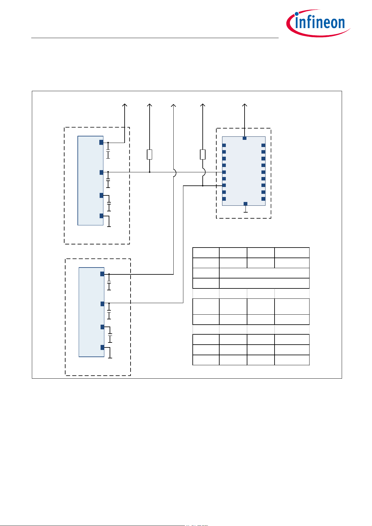
4 Application circuit
Figure 4 shows the recommended application circuit for two TLE4999C8 sensors.
Figure 4 Application circuit
Attention: The system integrator shall take in consideration that the maximum value of CL shall include
also the capacitance of the bus line.
Note: For improved EMC capability the usage of a twisted cable is recommended.
Data Sheet 7 v01_00
2020-11-02
Page 8
TLE4999C8
Programmable dual channel linear Hall sensor with fast SPC interface
Maximum ratings
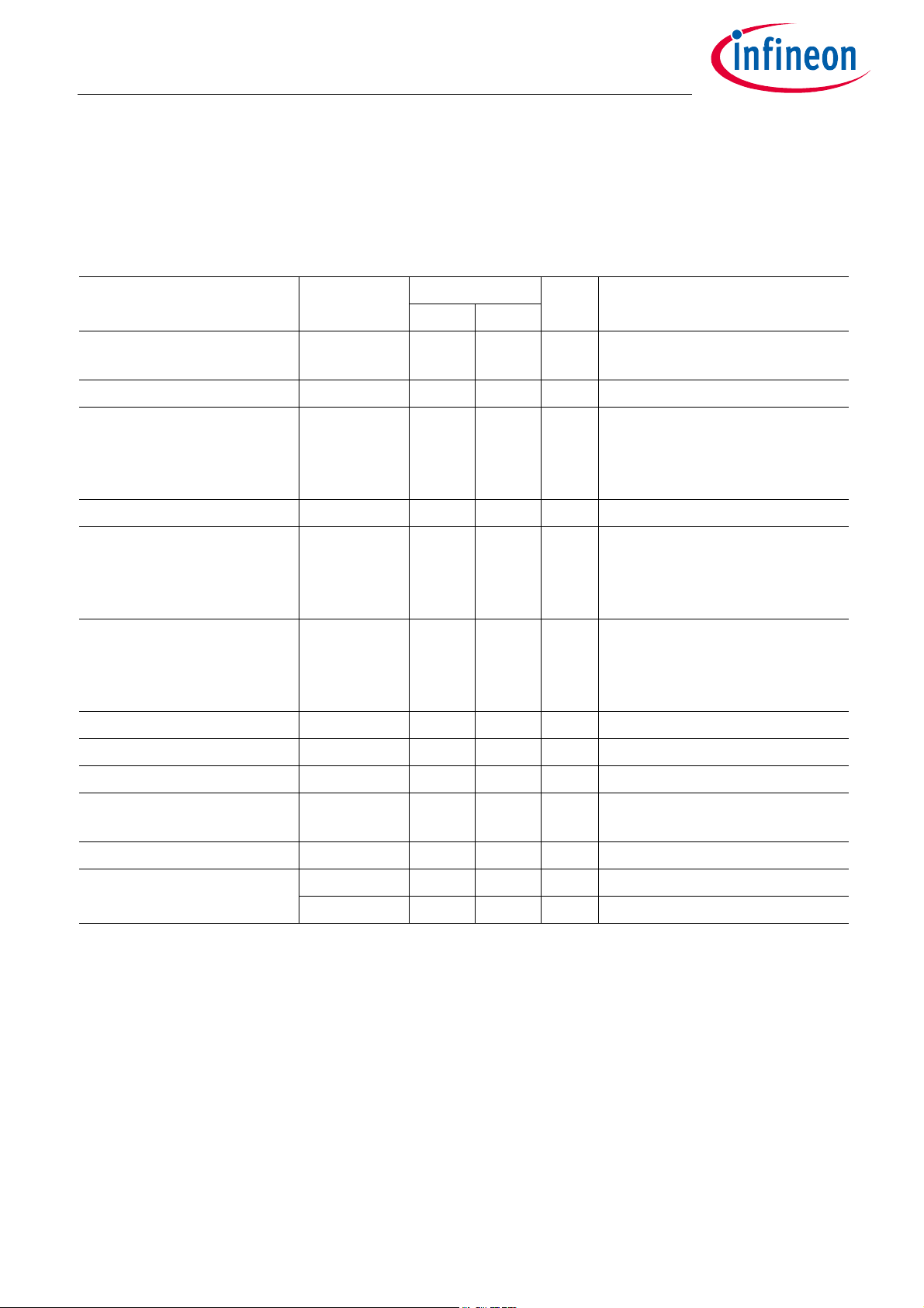
5 Maximum ratings
All specifications are valid over the full temperature range and over lifetime. They refer to each of the
implemented sensors IC’s, unless otherwise noted.
Table 3 Absolute maximum ratings
Parameter Symbol Limit Values Unit Notes
Min.
Max.
Junction temperature T
Non-operating temperature T
Maximum supply voltage V
Maximum voltage on OUT V
Maximum voltage on C
Buf
Maximum voltage between 2
V
V
J
NO
DD
OUT
Cbuf
Diff
pins
Voltage peaks VDD, V
OUT short circuit current
Supply current in over voltage I
Supply current in reverse
2)
I
OUT
DD, ov
I
DD, rev
voltage
OUT
-40 140 °C max. 1000h at 140°C1) (not
additive)
-40 125 °C max. 1400h (not additive)
1)
-20 20 V max. 24 h for -40°C to 30°C T
max. 10 min. for 30°C to 80°C T
max. 30 s for 80°C to 125°C T
max. 15 s above 125°C T
J
-18 19.5 V max. 40 h (not additive)
-0.3 20 V max. 24 h for -40°C to 30°C T
max. 10 min. for 30°C to 80°C T
max. 30 s for 80°C to 125°C T
max. 15 s above 125°C T
J
-20 20 V max. 24 h for -40°C to 30°C T
max. 10 min. for 30°C to 80°C T
max. 30 s for 80°C to 125°C T
max. 15 s above 125°C T
J
– 30 V for max. 50 µs
-130 130 mA max. 1 h
45 mA time limitation for VDD applies
-75 – mA time limitation for VDD applies
J
J
J
J
J
J
J
J
J
Magnetic flux density B
ESD Immunity V
1) Maximum exposure time at other junction temperatures shall be calculated using the Arrhenius-model.
2) Short to VDD or GND.
3) Human Body Model (HBM) according to ANSI/ESDA/JEDEC JS-001.
4) Charged Device Model (CDM) according to ANSI/ESDA/JEDEC JS-002.
max
HBM
V
CDM
– 1000 mT
-4 +4 kV Human Body Model
3)
-0.75 +0.75 kV Charged Device Model
4)
Note: Any stress exceeding the values listed in Table 3 may cause permanent damage to the device. The
values given are stress ratings only and functional operation of the device at these conditions is not
implied. Exposure to absolute maximum rating conditions for extended periods may affect device
reliability.
Data Sheet 8 v01_00
2020-11-02
Page 9

TLE4999C8
Programmable dual channel linear Hall sensor with fast SPC interface
Operating range
6 Operating range
The following operating conditions shall not be exceeded in order to ensure correct operation of the
TLE4999C8. All parameters specified in the following sections refer to these operating conditions.
Table 4 Operating range
Parameter Symbol
Supply voltage V
Supply voltage slew rate V
Operating junction
DD
DD,slew
T
J
temperature
Output pull-up voltage V
Pull-up resistance R
Load capacitance C
Supply capacitance C
Buffer capacitor C
pull-up
P
L
S
Buf
Min.
4.5 – 5.5 V
V
DD, pon
0.1 – 10
-40 – 140 °C max. 1000h at 140°C
3.04)/4.5
1.45 2.2 10 kΩ
1–3.9nF
– 100 – nF
–68–nF
Values
Unit Notes
Typ. Max.
–V
DD, poff
8
VExtended range
V/s
– 5.5V
1)
2)
3)
(not additive)
5)6)
7)
7)
Magnetic flux density |B| – – 50 mT Maximum measurement range
1) No magnetic performance degradation in extended range between supply under voltage release level and supply
over voltage release level.
2) The slew rate is the maximum voltage change per time and relates to the Application circuit.
3) Maximum exposure time at other junction temperatures shall be calculated using the Arrhenius-model.
4) Value valid only when the 3.3V bus capability bit is set in the EEPROM.
5) Output protocol characteristics depend on these parameters, RL must be according to max. output current. For the
maximum output pull up voltage value refer to the note on Table 3.
6) The SPC output protocol will be deactivated when permanent voltages higher then 7.5V are present at the OUT pin.
7) Pull-up resistance and load capacitance have to be chosen in accordance with configured unit time, please see
Application circuit.
6.1 Calculation of the junction temperature
The internal power dissipation P
temperature (TA).
The power multiplied by the total thermal resistance R
junction temperature. R
is the sum of the addition of the two components, Junction to Case and Case to
thJA
Ambient.
R
thJA=RthJC
TJ=TA +Δ T = R
+R
thCA
thJA
xP
TOT
= R
thJA
Example (assuming no load on V
• VDD = 5.5 V
• IDD = 14.5mA
•
Δ T= 150 [K/W] x (5.5 [V] x 0.0145 [A] + 0 [VA]) = 11.963K → 15K used for worst case scenario calculations
Data Sheet 9 v01_00
of the sensor increases the chip junction temperature above the ambient
TOT
(junction to ambient) added to TA leads to the final
thJA
x(VDD x IDD +V
):
OUT
OUT
x I
OUT
); IDD, I
> 0, if direction is into IC
OUT
2020-11-02
Page 10

TLE4999C8
Programmable dual channel linear Hall sensor with fast SPC interface
Electrical, magnetic and output parameters
7 Electrical, magnetic and output parameters
All specifications are valid over the full temperature range and over lifetime. They refer to each of the
implemented sensors IC’s, if not otherwise noted.
Table 5 Electrical characteristics
Parameter Symbol
Supply current I
Thermal resistance
Power-on time
1)
2)
Supply under voltage
DD
R
thJA
t
pon
V
DD, pon
reset/release level
Supply over voltage
V
DD, poff
reset/release level
Supply voltage reset
V
DD,pon hyst
hysteresis
Out pin over voltage
V
OUT, ov res
reset level
Out pin over voltage
V
OUT, ov res
release level
Out pin over voltage
V
OUT, ov hyst
reset hyteresis
Output saturation
V
OL
voltage
Min.
Values
Typ. Max.
Unit Notes
4 – 14.5 mA
– – 150 K/W junction to ambient
––5ms
3.1 – 4.2 V
6–7.5V
100 – 300 mV
7.5 8.25 9 V
6 6.75 7.5 V
11.52V
– – 0.1*VDD–for I
≤ 3.4mA
OUT
Output fall and rise time t
fall/trise
0.3 0.5 0.75 µs for UT = 0.5 µs and 0.75 µs
0.6 1 1.4 µs for UT = 1 µs and 1.25 µs
0.9 1.5 2.1 µs for UT = 1.5 µs
1.2 2 2.8 µs for UT = 2 µs and 2.5 µs
1.8 3 4.2 µs for UT = 3 µs
Output current I
Output leakage current I
Oscillator frequency
OUT,avg
OUT Leak
20 100 120 µA V
Δf -5 – 5 % Nominal oscillator frequency:
variation
1) Measured on 2s2p PCB board
2) Time since the sensor starts, until it is ready to respond to the first trigger pulse
5mA
pull-up
20MHz
= 5V and 0 < VDD< V
DD, pon
The following Figure 5 shows the operating area of the device, the condition for over voltage and
under voltage and the corresponding sensor reaction. The values for the over- and under voltage comparators
are the typical values from Table 5.
In the extended range, the sensor fulfills the full specification. However, voltages above the operating range
can only be applied for a limited time (see Table 3).
Data Sheet 10 v01_00
2020-11-02
Page 11

V
OUT
/ V
pull up
V
DD
4.2 6
7.5
3.1
9
No output
No output
No output
Operating
range
Extended range
Extended range
7.5
Vout
OV reset
V
DD
UV reset
V
DD
OV reset
Extended range
No output
3
1)
/ 4.5
Operating range
TLE4999C8
Programmable dual channel linear Hall sensor with fast SPC interface
Electrical, magnetic and output parameters
Figure 5 Operating area and sensor reaction for over- and under voltage.
1)
Main and Sub channels of the TLE4999C8 provide highly accurate 12/14/16bit magnetic field signals. The
output characteristics of the two channels are specified in Table 6.
Table 6 Magnetic and output characteristics of main and sub channel
Parameter Symbol
Magnetic offset drift
Magnetic initial offset B
Magnetic sensitivity drift
Output noise (RMS)
Magnetic hysteresis B
Integral non-linearity
Signal latency
1) Drift over temperature and lifetime
2) For LP-Filter setting 8
3) Range 50 mT, gain 1.0 (scales linearly with gain)
4) Defined as phase shift of 100 Hz sine signal
5) For LP-Filter setting Off
Figure 6 shows the output characteristics of the sensor’s main and sub channel in the default setting. The
output characteristics can be changed by reconfiguring the zero point, gain and clamping ranges for main and
sub channel (see Chapter 9).
Value valid only when the 3.3V bus capability bit is set in the EEPROM.
Values
4)5)
1)
1)
2)3)
3)
Min.
ΔB
ΔB
OS_Main
OS_Sub
OS
-100 – 100 µT Main channel offset drift
-200 – 200 µT Sub channel offset drift
-300 – 300 µT at 0 h, 25 °C
ΔS -2.0 – 2.0 %
OUT
OUT
Hys
Noise_Main
Noise_Sub
––1LSB12Main channel noise
––4LSB12Sub channel noise
––40µT
INL -4 – 4 LSB
t
latency
– – 200 µs not including interface
Typ. Max.
Unit Notes
12
transmission time
Data Sheet 11 v01_00
2020-11-02
Page 12

Magnetic Flux B [mT]
Sensor Signal [LSB
12
]
-50 500
2048
0
4095
Main clamping
Sub clamping
4095
205
Branded Side
N
S
Main Channel
Sub Channel
3890
TLE4999C8
Programmable dual channel linear Hall sensor with fast SPC interface
Electrical, magnetic and output parameters
Figure 6 Output characteristic
Data Sheet 12 v01_00
2020-11-02
Page 13

Sub Hall data (12 bi t)
Sync Fr ameTrigger Pulse
µC Activity
Sensor Ac tivity
13 UT / 90 UT
56 UT 12 … 27 UT 12 … 27 UT 12 … 27 UT 12 … 27 UT
12 UT
Status Nibble
Data Nibble 1
Data Nibble 3
Data N ibble 2
End
Pulse
12 … 27 UT 12 … 27 UT 12 … 27 UT
Data Nibble 4 Data Nibble 6
Data N ibble 5
CRC Nibble
12 … 27 UT
Main H all data (12 bi t)
Nibble Encoding: (12 + x) * UT
TLE4999C8
Programmable dual channel linear Hall sensor with fast SPC interface
SPC output
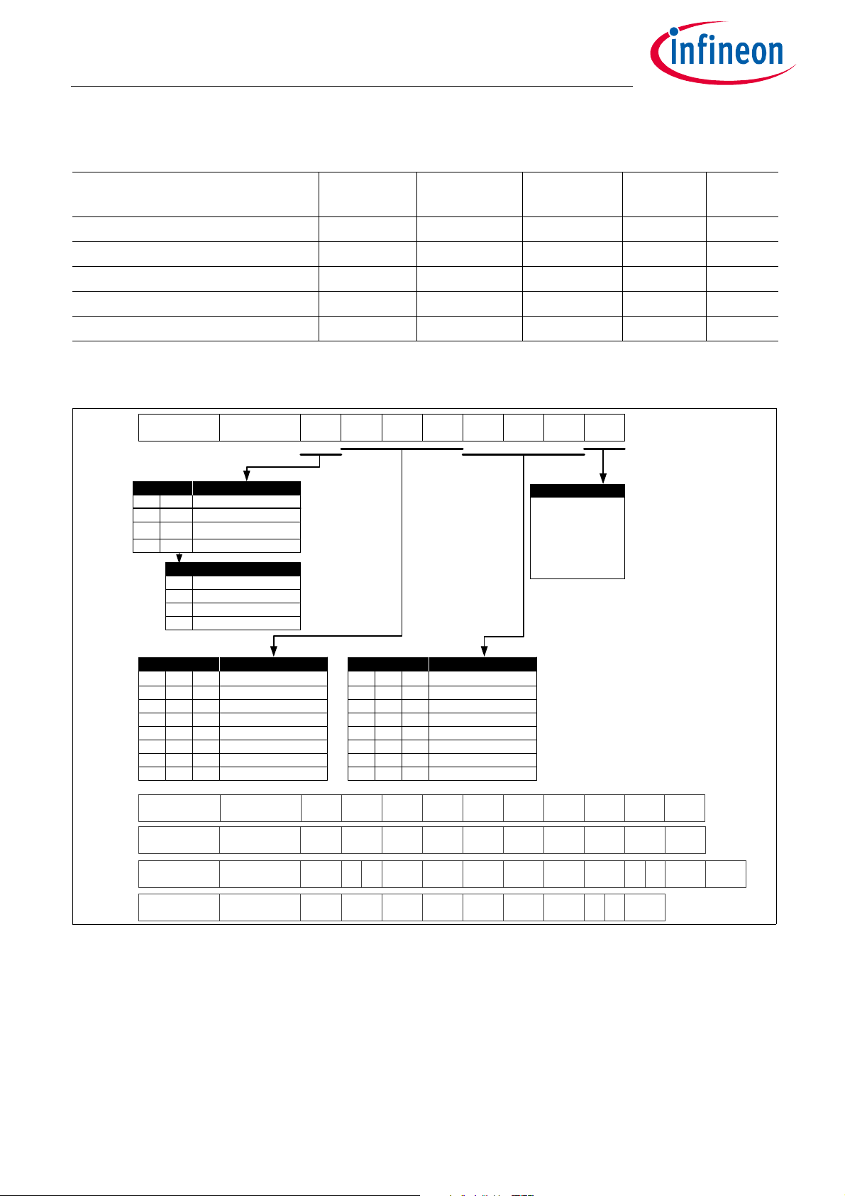
8 SPC output
The TLE4999C8 features a fast SPC (Short PWM Code) protocol, which is based on the SENT standard (Single
Edge Nibble Transmission) defined by SAE J2716. As opposed to SENT, which implies a continuous
transmission of data, the SPC protocol transmits data only after receiving a specific trigger pulse from the
micro controller. The required length of the trigger pulse depends if the sensor is configured in synchronous
mode or in bus mode. In case of bus mode the trigger pulse depends on the sensor number, which is
configurable. Thereby, SPC allows the operation of up to four sensors on one bus line.
For the SPC interface the push pull setting with controlled slopes is used (the push-pull mode is only active
during the slope controlled mode). In this configuration, the TLE4999C8 has controlled rising and falling
slopes. Between the slope controlled transitions the HIGH level is maintained by the external pull-up resistor.
Once the SPC protocol telegram is sent, the TLE4999C8 goes in to receiving mode (OUT Pin in Tri-sate mode)
and waits until a valid trigger signal is received.
Figure 7 SPC default protocol example
As in the SENT protocol, the time between two consecutive falling edges defines the value of a 4-bit nibble,
thus representing numbers between 0 and 15. The transmission time therefore depends on the transmitted
data values. All values are multiples of a unit time frame (see Table 8). A SPC frame consists of the following
nibbles (see Table 7):
• A trigger pulse by the master, which initiates the data transmission.
• A synchronization period of 56 UT.
• A st atus nibble of 12-27 UT, contai ning over volta ge/ error signaling and short serial message (SSM) data or
the sensor ID.
• Between 3 and 4 data nibbles of 12-27 UT each (number is programmable), representing the Main Hall
value
• Between 3 and 4 data nibbles of 12-27 UT each (number is programmable), representing the Sub Hall
value.
• Optional 2 temperature nibbles of 12-27 UT each (programmable).
• Optional 2 /4 bit rolling counter of 12-27 UT (programmable).
• One or two checksum (CRC) nibbles of 12-27 UT each (programmable).
• An end pulse of 12 UT to terminate the SPC frame transmission.
The sensor is available for the next sample after the falling edge of the end pulse. The sensor’s sampling
time is at the beginning of the synchronization period, i.e. when a correct trigger is received.
Data Sheet 13 v01_00
2020-11-02
Page 14
11111111 1110 4094
11111111 1101 4093
:: : :
00000000 0010 2
00000000 0001 1
00000000 0000 0
11111111
M1 M2 M3 S3 S2 S1
bits description
MSBs LSBs stat us informatio n
10
SSM/ID
01
00
startup/internal error main
internal error sub/return from
overvoltage
normal operation
bits
M3
1111
M2M1
description
Main Hall value (12 bit)
4095
SYNC ST ATUS CRC
description
CRC calculation
for all nibbles
seed value: 0101
polynomial: X
4+X3 +X2
+1
SSM/ID
SSM/ID
TRIGGER
11111111 1110 4094
11111111 1101 4093
:: : :
00000000 0010 2
00000000 0001 1
00000000 0000 0
11111111
bits
S3
1111
S2S1
description
Sub Hall value (12 bit)
4095
Frame
A
bits description
11
01
00
SSM or ID #3
SSM or ID #0
SSM or ID #1
10 SSM or ID #2
TRIGGER
Frame
B
S2M1 S1 CRC
S2TRIGGER
Frame
D
S4
CRC CRCS1
TRIGGER
Frame
E
M1
CR
C
TRIGGER
Frame
C
M1 T1 CRCT2
CRCRC
SYNC
SYNC
SYNC
SYNC
STATUS
STATUS
STATUS
STATUS
RC
1
M1
M2
M2
M2
M2
M3
M3
M3
M3
M4
S3
M4
S3
S4
S2
RC
2
S2
S3
S1
S3
S1
TLE4999C8
Programmable dual channel linear Hall sensor with fast SPC interface
SPC output
Table 7 Frame selection
Frame Type Parameter F Data nibbles Temperature
nibbles
Rolling
Counter
CRC bits
12 bit Main Hall, 12 Bit Sub Hall A (default) 6 nibbles – – 4 bits
16 bit Main Hall, 16 Bit Sub Hall B 8 nibbles – – 4 bits
12 bit Main Hall, 12 bit Sub Hall C 6 nibbles 2 nibbles – 4 bits
14 bit Main Hall, 14 bit Sub Hall D 7 nibbles – 2 x 2 bits
12 bit Main Hall, 12 Bit Sub Hall E 6 nibbles – 2 bits
1) Rolling counters combined with data nibbles, see Figure 8
2) Rolling counter combined with CRC nibble, see Figure 8
1)
8 bits
2)
6 bits
Figure 8 Content of the SPC protocol
8.1 SPC bus mode
When the sensor is used in a bus mode with other sensors on a common SPC line, individual addresses have
to be assigned to each sensor for identification. For the operation of the sensor in a SPC bus mode, it is strongly
recommended that the sensor ID is written into the EEPROM of the sensor, as all sensors are pre configured
with the default value “ID = 0” (see the TLE4999C User Manual for further details).
A corresponding trigger nibble from the micro controller can therefore address each sensor individually.
Data Sheet 14 v01_00
2020-11-02
Page 15

SPC
V
th, falling
t
mlow
t
mtr
V
th, rising
TLE4999C8
Programmable dual channel linear Hall sensor with fast SPC interface
SPC output
The trigger nibble low time is shown in Table 10. Each low time corresponds to an individual sensor address.
The total length of the trigger nibble can be selected to be constant at 90 UT (constant trigger length) or
variable according to Table 9(variable trigger length).
8.2 SPC unit times
Table 8 Programmable unit times
Parameter Symbol Values Unit Note or Test Condition
SPC unit time
1) Default setting is 3 μs nominal SPC unit time.
8.3 SPC trigger pulse
A SPC transmission is initiated by a trigger pulse from the ECU on the OUT pin. To detect a low-level on the
OUT pin, the voltage has to be below the threshold V
released as soon as V
The master low time t
mode switched off, the total trigger time t
transmission time for configurations where only one sensor IC is connected to the SPC line.
With bus mode switched on, it is possible to use up to four SPC sensors on one data line. The total trigger time
in bus mode is longer, and can be selected between a constant trigger or a variable trigger.
The master low time t
addressing requires all sensors on the bus to be programmed with the same nominal SPC unit time.
1)
UT 0.5, 0.75, 1.0, 1.25, 1.5, 2.0, 2.5, 3.0 μs Clkunit=20MHz
. The sensor detects that the OUT line has been
th, falling
is crossed. Table 9 and Figure 9 show the timing specification for the trigger pulse.
th, rising
as well as the total trigger time t
mlow
is shortest. This leads to a significantly shorter overall protocol
mtr
is used to identify the sensor ID of the addressed sensor IC, see Table 10. A proper
mlow
are different for SPC bus mode on or off. With bus
mtr
Figure 9 SPC master pulse timing
Table 9 SPC master pulse parameters
Parameter Symbol Values Unit Note or Test Condition
Falling edge threshold V
Rising edge threshold V
Data Sheet 15 v01_00
thf
thr
Min. Typ. Max.
–35 –% of
V
DD
–50 –% of
V
DD
1)2)
1)2)
2020-11-02
Page 16

TLE4999C8
Programmable dual channel linear Hall sensor with fast SPC interface
SPC output
Table 9 SPC master pulse parameters (cont’d)
Parameter Symbol Values Unit Note or Test Condition
Min. Typ. Max.
Total trigger time t
mtr
–13 –UTBus mode off
– 90 – UT Bus mode on, with
constant trigger length
3)
2)
–t
1) Not subject to production test - verified by design/characterization
2) Unit is % of nominal VDD (4.5V - 5.5V)
3) Trigger time in the sensor is fixed to the number of unit times specified in the “typ.” column, but the effective trigger
time varies due to the sensor’s oscillator variation
mlow,min
+ 12– UT Bus mode on, with
variable trigger length
2)
The below Table 10 shows the trigger time window to which the sensor responds:
Table 10 Sensor SPC trigger parameters
Parameter Symbol Values Unit Note or Test Condition
Min. Typ. Max.
Master nibble low time t
Master nibble low time t
Master nibble low time t
Master nibble low time t
Master nibble low time t
1) The combination of CL and pull-up resistor Rp may prevent use of some master nibble low times due to increased
output rise time. Infineon recommends that for fast unit times (<=1.0us) the sensor is used in bus mode (with variable
trigger option) with ID0 instead of bus mode off.
mlow
mlow
mlow
mlow
mlow
2 – 7 UT Bus mode off
8 – 15 UT Bus mode on, ID = 0
16 – 28 UT Bus mode on, ID = 1
29 – 49 UT Bus mode on, ID = 2
50 – 82 UT Bus mode on, ID = 3
1)
The below Table 11 shows the trigger time window to be programmed in the ECU:
Table 11 ECU SPC trigger parameters
Parameter Symbol Values Unit Note or Test Condition
Min. Typ. Max.
Master nibble low time t
Master nibble low time t
Master nibble low time t
Master nibble low time t
Master nibble low time t
1) The combination of CL and pull-up resistor Rp may prevent use of some master nibble low times due to increased
output rise time. Infineon recommends that for fast unit times (<=1.0us) the sensor is used in bus mode (with variable
trigger option) with ID0 instead of bus mode off.
mlow
mlow
mlow
mlow
mlow
2 – 4 UT Bus mode off
9 – 12 UT Bus mode on, ID = 0
19 – 23 UT Bus mode on, ID = 1
35.5 – 40.5 UT Bus mode on, ID = 2
61.5 – 67.5 UT Bus mode on, ID = 3
1)
Attention: For detailed description of the master nibble low times, please consult the application note for
the TLE4999C, “Master nibble low time parameter and related tolerances”.
Data Sheet 16 v01_00
2020-11-02
Page 17

TLE4999C8
Programmable dual channel linear Hall sensor with fast SPC interface
SPC output
8.4 Status nibble
The status nibble consists of 4 bits. The first two bits are status bits to monitor the internal status of the sensor
whereas the last two bits can represent a short serial message (see Chapter 8.5) or the sensor ID. Table 12
shows the usage of the status bits.
The status nibble, which is sent with each SPC data frame, provides an error indication. In case the sensor
detects an error or an over voltage condition, the corresponding error bit in the status nibble is set. As long
as the error or over voltage condition is present the error bit is set and the sensor output is disabled. After
returning from the over voltage condition the corresponding error bit is set in the first transmitted frame in the
status nibble.
Table 12 Structure of SPC status nibble
Bits Description
[0] LSB
[1]
[2]
[3] MSB
Short Serial Message bit (data) or bus mode ID LSB
Short Serial Message bit (start indication) or bus mode ID MSB
Return from over voltage condition/ internal error sub channel
Startup/ internal error main channel
8.5 Short serial message
The short serial message is an additional option which can be enabled or disabled. The short serial message
provides additional information in a slow channel transmitting an 8 bit temperature value of the main hall and
32 bit sensor ID (16 bits from main channel ID1 and 16 bits from sub channel ID2).
In each SPC frame, one bit of information is transmitted. The start of the short serial message is indicated by
a “1” in bit [1] of the status nibble. For the next 15 SPC frames, this bit will contain a “0”. The Information is
transmitted in blocks of 16 bit with 1 bit per SPC frame in bit [0] of the status nibble.
4 bit message ID
8 bit data
4bit CRC (calculated from message ID and data bits)
The message ID is used for identification of the type of data received. All data are transmitted in the bit [0] of
the status nibble in the order MSB to LSB.
The transmitted information is as follows:
Message -ID 0: 8 bit temperature value starting with MSB
Message -ID 1: 8 bit of sensor ID1 (starting with MSB)
Message -ID 2: 8 bit of sensor ID1 (starting with MSB-8)
Message -ID 3: 8 bit of sensor ID2 (starting with MSB)
Message -ID 4: 8 bit of sensor ID2 (starting with MSB-8)
Note: For further details please see the TLE4999C User Manual.
Data Sheet 17 v01_00
2020-11-02
Page 18

TLE4999C8
Programmable dual channel linear Hall sensor with fast SPC interface
SPC output
8.6 Temperature nibbles
The temperature is coded as an 8 bit value. The value is transferred in unsigned integer format and
corresponds to the range between -55 °C and +200 °C, so a transferred value of 55 corresponds to 0 °C. The
temperature is additional information and although it is not calibrated, may be used for a plausibility check,
for example. Table 13 shows the mapping between junction temperature and the transmitted value in the
SPC frame.
Table 13 Mapping of Temperature Value
Junction Temperature Typ. Decimal Value from Sensor Note
- 55 °C 0 Theoretical lower limit
0°C 55 –
25 °C 80 –
200 °C 255 Theoretical upper limit
1) Theoretical range of temperature values, not operating temperature range.
1)
1)
8.7 Rolling Counter
The rolling counter is an additional option for a safety check implementation. Therefore the counter counts
the number of transmitted frames with rollover back to 0 and increments with each message. The ECU can use
this data for verification that no frame is missed or that no frame is sent repeatedly from the sensor.
There are two selectable protocols that include the rolling counter (see Figure 8), on frame D a 2 bit rolling
counter is included in the first main data nibble and another 2 bit rolling counter in the first sub data nibble.
On frame E a 2 bit rolling counter is included in the CRC nibble, further details can be found in Chapter 8.8.
There are frames without rolling counter bits, but to meet the safety requirements and target ASIL level of the
application, it is recommended to use this function.
8.8 CRC nibble
The CRC checksum can be used to check the validity of the decoded data. In the checksum included is the
status nibble and the data nibbles. It is calculated using a polynomial(x
The remainder after the last data nibble is transmitted as CRC.
To allow enhanced checksum for higher diagnostic coverage also 6 and 8 bit checksum are available to secure
the data transmission (see Table 7).
The 6 bit checksum is calculated using a polynomial (x
checksum is calculated using a polynomial (x
The calculation scheme of the CRC is described in detail in the TLE4999C User Manual.
8
+ x5+ x3 + x2 + x + 1) with a seed value of 01010101B.
6
+ x + 1) with a seed value of 010101B and the 8 bit
4
+ x3 + x2 + 1) with a seed value of 0101B.
8.9 SPC frameholder
The frameholder functionality allows the user to operate multiple sensors in a bus configuration with
synchronized sampling of the measurement value. This is achieved by having (apart from the SPC Bus ID) a
separate frameholder ID for each chip on the bus which is used as a common signal trigger.
For further information please see TLE4999C User Manual.
Data Sheet 18 v01_00
2020-11-02
Page 19

TLE4999C8
Programmable dual channel linear Hall sensor with fast SPC interface
Configuration and calibration parameters
9 Configuration and calibration parameters
To perform the EEPROM programming with application and customer specific data the Serial Inspection and
Configuration Interface (SICI) is used. The single wire interface uses the same pin as the SPC output for
communication.
The TLE4999C8 has several configurable parameters which are stored in the EEPROM. These parameters affect
the internal data processing and the output protocol. Table 14 gives an overview of the magnetic
measurement parameters, which can be configured separately for main and sub channel. Table 15 shows the
SPC interface parameters.
Table 14 TLE4999C8 Magnetic measurement parameters for main and sub Channel
Parameter Setting range Note
Magnetic range ±50 mT (default)
±25 mT
Gain -7.59...7.59
Gain value of +1.0 corresponds to typical 36.875
LSB
/mT sensitivity in 50mT range, with ±5%
12
clamping,(73.75 LSB
/mT in 25mT range, with
12
±5% clamping).
Zero point 0 LSB
... 65535 LSB
16
1)
16
The user zero point setting is independently
configurable for main and sub channels with 12,
14 or 16 bit granularity.
Clamping low level 0 LSB
... 65535 LSB
16
Clamping high level 0 LSB16 ... 65535 LSB
Default setting: 32768 LSB
1)
16
1)
16
Output clamping settings, see Figure 6.
Default setting:
CL: 205 LSB
CH: 3890 LSB
16
16
.
16
Multi point linearization 0 ... 9 point 9 user selectable linearization points
configurable in the EEPROM. The user can select
the concentration either at the corners or
around the middle point. For further details
please see the TLE4999C User Manual.
Low-pass filter
2)
0: Off
3)
Low pass filter cut-off (-3 dB) frequency.
1: 80Hz
2: 160 Hz
3: 200 Hz
4: 240 Hz
5: 320 Hz
6: 400 Hz
7: 470 Hz
8: 500 Hz (default)
9: 650 Hz
10: 870 Hz
11: 980 Hz
12: 1070 Hz
13: 1270 Hz
14: 1380 Hz
15: 1530 Hz
Data Sheet 19 v01_00
2020-11-02
Page 20

TLE4999C8
Programmable dual channel linear Hall sensor with fast SPC interface
Configuration and calibration parameters
Table 14 TLE4999C8 Magnetic measurement parameters for main and sub Channel
Parameter Setting range Note
st
order temperature
1
coefficient TC
nd
order temperature
2
coefficient TC
4)
1
4)
2
Reference Temperature
T
0
1) The internal value is always 16 bit, in case the 12 or 14 bit setting range is used, the output will be clamped
accordingly.
2) Subject to oscillator variation ±5%.
3) Set programmable low pass filter off, inherent filter of ADC stays on.
4) Adjusting the temperature coefficients (TC1 & TC2) can lead to a slight increase of the ADC noise level.
-2400 ppm/°C ... 5400 ppm/°C Second order user configurable temperature
compensation.
-30 ppm/°C2 ... 30 ppm/°C
2
0°C ... 127°C
Table 15 TLE4999C8 SPC Interface parameters
Parameter Setting range Note
SPC protocol frames 2x 12 bit Hall + 4 bit CRC (default)
see Table 7
2x 16 bit Hall +4 bit CRC
2x 12 bit Hall + 8 bit temperature + 4 bit CRC
2x 14 bit Hall + 2x 2 bit RC + 8 bit CRC
2x 12 bit Hall + 2 bit RC + 6 bit CRC
SPC unit time
1)
0.5 µs ... 3.0 µs See chapter Chapter 8.2
SPC bus mode On
See chapter Chapter 8.1
Off (default)
SPC bus pull-up voltage 3.3V/5V Default 5V
SPC ID 0 ... 3 Default ID0
SPC variable trigger On
Off (default)
SPC frameholder
address
1) Subject to oscillator variation ±5%.
2) The SPC frameholder is deactivated in case the frameholder address is equal to the SPC address.
2)
0 ... 3 Default ID0
Data Sheet 20 v01_00
2020-11-02
Page 21

TLE4999C8
Programmable dual channel linear Hall sensor with fast SPC interface
Package outlines
10 Package outlines
Figure 10 PG-TDSO (Plastic Green Thin Dual Small Outline), package dimensions
10.1 Distance of chip to package
Figure 11 shows the distance of the chip surface to the TLE4999C8 surface.
Figure 11 Distance of chip surface to package surface
10.2 Moisture Sensitivity Level (MSL)
The TLE4999C8 fulfills the MSL level 3 according to IPC/JEDEC J-STD-033B.1.
Data Sheet 21 v01_00
2020-11-02
Page 22

For further information on alternative packages, please visit our website:
http://www.infineon.com/packages.
Dimensions in mm
TLE4999C8
Programmable dual channel linear Hall sensor with fast SPC interface
Package outlines
10.3 Package marking
Figure 12 PG-TDSO (Plastic Green Thin Dual Small Outline), package marking
Data Sheet 22 v01_00
2020-11-02
Page 23

TLE4999C8
Programmable dual channel linear Hall sensor with fast SPC interface
Package outlines
Green Product (RoHS compliant)
To meet the world-wide customer requirements for environmentally friendly products, and to be compliant
with government regulations the device is available as a green product. Green products are RoHS Compliant
(i.e Pb free finish on leads and suitable for Pb free soldering according to IPC/JEDEC J-STD-020).
Data Sheet 23 v01_00
2020-11-02
Page 24

TLE4999C8
Programmable dual channel linear Hall sensor with fast SPC interface
Terminology
A
ADC Analog to digital converter
B
BIST Built-in self-test
C
CBUF Buffer capacitor
CRC Cyclic redundancy check
D
DSP Digital Signal Processing unit
E
ECC Error correction code to protect EEPROM content
EEPROM
(abbrev. EEP)
G
GND Ground - ground line of sensor
H
HADC Hall analog to digital converter
Electrically erasable and programmable read only memory - programmable memory for
sensor calibration and configuration data
HTS-ADC Hall, temperature, stress analog to digital converter
I
ID Identification
L
LP-Filter Low pass filter
LSB Least significant bit
M
MSB Most significant bit
MVS Margin voltage selector
O
OUT Digital output pin of the sensor
P
PWM Pulse Width Modulation
R
RMS Root mean square
ROM Read only memory
S
SICI Serial Inspection and Configuration Interface - Programming interface of the TLE4999C8
SPC Short PWM Code
Data Sheet 24 v01_00
2020-11-02
Page 25

TLE4999C8
Programmable dual channel linear Hall sensor with fast SPC interface
Revision History
11 Revision History
Revision Date Changes
01.00 2020-11-02 Initial release
Data Sheet 25 v01_00
2020-11-02
Page 26

Trademarks
All referenced product or service names and trademarks are the property of their respective owners.
IMPORTANT NOTICE
Edition 2020-11-02
Published by
Infineon Technologies AG
81726 Munich, Germany
© 2020 Infineon Technologies AG.
All Rights Reserved.
Do you have a question about any
aspect of this document?
Email: erratum@infineon.com
Document reference
The information given in this document shall in no
event be regarded as a guarantee of conditions or
characteristics ("Beschaffenheitsgarantie").
With respect to any examples, hints or any typical
values stated herein and/or any information regarding
the application of the product, Infineon Technologies
hereby disclaims any and all warranties and liabilities
of any kind, including without limitation warranties of
non-infringement of intellectual property rights of any
third party.
In addition, any information given in this document is
subject to customer's compliance with its obligations
stated in this document and any applicable legal
requirements, norms and standards concerning
customer's products and any use of the product of
Infineon Technologies in customer's applications.
The data contained in this document is exclusively
intended for technically trained staff. It is the
responsibility of customer's technical departments to
evaluate the suitability of the product for the intended
application and the completeness of the product
information given in this document with respect to
such application.
For further information on technology, delivery terms
and conditions and prices, please contact the nearest
Infineon Technologies Office (www.infineon.com).
WARNINGS
Due to technical requirements products may contain
dangerous substances. For information on the types
in question please contact your nearest Infineon
Technologies office.
Except as otherwise explicitly approved by Infineon
Technologies in a written document signed by
authorized representatives of Infineon Technologies,
Infineon Technologies’ products may not be used in
any applications where a failure of the product or any
consequences of the use thereof can reasonably be
expected to result in personal injury.
 Loading...