

Page 1
Data Sheet, V 2.10, April 2020
TLE4997E2
Programmable Linear Hall Sensor
Sensors
Never stop thinking.
Page 2

Edition 2020-04
Published by Infineon Technologies AG,
Am Campeon 1-12,
85579 Neubiberg, Germany
© Infineon Technologies AG 2020.
All Rights Reserved.
Attention please!
The information herein is given to describe certain components and shall not be considered as a guarantee of
characteristics.
Terms of delivery and rights to technical change reserved.
We hereby disclaim any and all warranties, including but not limited to warranties of non-infringement, regarding
circuits, descriptions and charts stated herein.
Information
For further information on technology, delivery terms and conditions and prices please contact your nearest
Infineon Technologies Office (www.infineon.com).
Warnings
Due to technical requirements components may contain dangerous substances. For information on the types in
question please contact your nearest Infineon Technologies Office.
Infineon Technologies Components may only be used in life-support devices or systems with the express written
approval of Infineon Technologies, if a failure of such components can reasonably be expected to cause the failure
of that life-support device or system, or to affect the safety or effectiveness of that device or system. Life support
devices or systems are intended to be implanted in the human body, or to support and/or maintain and sustain
and/or protect human life. If they fail, it is reasonable to assume that the health of the user or other persons may
be endangered.
Page 3

TLE4997E2
We Listen to Your Comments
Any information within this document that you feel is wrong, unclear or missing at all?
Your feedback will help us to continuously improve the quality of this document.
Please send your proposal (including a reference to this document) to:
sensors@infineon.com
Revision History: 2020-04 V2.10
Previous Version: V 2.09, January 2018
Page Subjects (major changes since last revision)
All Updated product name to TLE4997E2
16 Table 5: removed unintended content
Page 4

TLE4997E2
Table of Contents Page
1Overview . . . . . . . . . . . . . . . . . . . . . . . . . . . . . . . . . . . . . . . . . . . . . . . . . . . 7
1.1 Features . . . . . . . . . . . . . . . . . . . . . . . . . . . . . . . . . . . . . . . . . . . . . . . . . . . . 7
1.2 Target Applications . . . . . . . . . . . . . . . . . . . . . . . . . . . . . . . . . . . . . . . . . . . 8
1.3 Pin Configuration . . . . . . . . . . . . . . . . . . . . . . . . . . . . . . . . . . . . . . . . . . . . . 8
2 General . . . . . . . . . . . . . . . . . . . . . . . . . . . . . . . . . . . . . . . . . . . . . . . . . . . . 9
2.1 Block Diagram . . . . . . . . . . . . . . . . . . . . . . . . . . . . . . . . . . . . . . . . . . . . . . . 9
2.2 Functional Description . . . . . . . . . . . . . . . . . . . . . . . . . . . . . . . . . . . . . . . . . 9
2.3 Principle of Operation . . . . . . . . . . . . . . . . . . . . . . . . . . . . . . . . . . . . . . . . 10
2.4 Further Notes . . . . . . . . . . . . . . . . . . . . . . . . . . . . . . . . . . . . . . . . . . . . . . . 10
2.5 Transfer Functions . . . . . . . . . . . . . . . . . . . . . . . . . . . . . . . . . . . . . . . . . . . 11
3 Maximum Ratings . . . . . . . . . . . . . . . . . . . . . . . . . . . . . . . . . . . . . . . . . . 12
4 Operating Range . . . . . . . . . . . . . . . . . . . . . . . . . . . . . . . . . . . . . . . . . . . 13
5 Electrical and Magnetic Parameters . . . . . . . . . . . . . . . . . . . . . . . . . . . 14
6 Signal Processing . . . . . . . . . . . . . . . . . . . . . . . . . . . . . . . . . . . . . . . . . . 17
6.1 Magnetic Field Ranges . . . . . . . . . . . . . . . . . . . . . . . . . . . . . . . . . . . . . . . 18
6.2 Gain Setting . . . . . . . . . . . . . . . . . . . . . . . . . . . . . . . . . . . . . . . . . . . . . . . . 19
6.3 Offset Setting . . . . . . . . . . . . . . . . . . . . . . . . . . . . . . . . . . . . . . . . . . . . . . . 19
6.4 DSP Input Low Pass Filter . . . . . . . . . . . . . . . . . . . . . . . . . . . . . . . . . . . . . 20
6.5 DAC Input Interpolation Filter . . . . . . . . . . . . . . . . . . . . . . . . . . . . . . . . . . 22
6.6 Clamping . . . . . . . . . . . . . . . . . . . . . . . . . . . . . . . . . . . . . . . . . . . . . . . . . . 23
7 Error Detection . . . . . . . . . . . . . . . . . . . . . . . . . . . . . . . . . . . . . . . . . . . . . 25
7.1 Voltages Outside the Operating Range . . . . . . . . . . . . . . . . . . . . . . . . . . . 25
7.2 Open Circuit of Supply Lines . . . . . . . . . . . . . . . . . . . . . . . . . . . . . . . . . . . 25
7.3 Not Correctable EEPROM Errors . . . . . . . . . . . . . . . . . . . . . . . . . . . . . . . 26
8 Temperature Compensation . . . . . . . . . . . . . . . . . . . . . . . . . . . . . . . . . . 27
8.1 Parameter Calculation . . . . . . . . . . . . . . . . . . . . . . . . . . . . . . . . . . . . . . . . 28
9Calibration . . . . . . . . . . . . . . . . . . . . . . . . . . . . . . . . . . . . . . . . . . . . . . . . 29
9.1 Calibration Data Memory . . . . . . . . . . . . . . . . . . . . . . . . . . . . . . . . . . . . . . 30
9.2 Programming Interface . . . . . . . . . . . . . . . . . . . . . . . . . . . . . . . . . . . . . . . 31
9.3 Laboratory Evaluation Programmer . . . . . . . . . . . . . . . . . . . . . . . . . . . . . . 31
10 Application Circuit . . . . . . . . . . . . . . . . . . . . . . . . . . . . . . . . . . . . . . . . . . 32
11 Package Outlines . . . . . . . . . . . . . . . . . . . . . . . . . . . . . . . . . . . . . . . . . . . 33
Data Sheet 4 V 2.10, 2020-04
Page 5

TLE4997E2
List of Figure s Page
Figure 1 Pin Configuration and Hall Cell Location . . . . . . . . . . . . . . . . . . . . . . . . 8
Figure 2 Block Diagram . . . . . . . . . . . . . . . . . . . . . . . . . . . . . . . . . . . . . . . . . . . . 9
Figure 3 Examples of Operation . . . . . . . . . . . . . . . . . . . . . . . . . . . . . . . . . . . . 11
Figure 4 Ratiometry Error Band . . . . . . . . . . . . . . . . . . . . . . . . . . . . . . . . . . . . . 15
Figure 5 Signal Processing Flow . . . . . . . . . . . . . . . . . . . . . . . . . . . . . . . . . . . . 17
Figure 6 DSP Input Filter (Magnitude Plot) . . . . . . . . . . . . . . . . . . . . . . . . . . . . 21
Figure 7 DAC Input Filter (Magnitude Plot) . . . . . . . . . . . . . . . . . . . . . . . . . . . . 22
Figure 8 Clamping Example. . . . . . . . . . . . . . . . . . . . . . . . . . . . . . . . . . . . . . . . 24
Figure 9 EEPROM Map . . . . . . . . . . . . . . . . . . . . . . . . . . . . . . . . . . . . . . . . . . . 30
Figure 10 Application Circuit . . . . . . . . . . . . . . . . . . . . . . . . . . . . . . . . . . . . . . . . 32
Figure 11 PG-SSO-3-10 (Plastic Green Single Small Outline Package) . . . . . . . 33
Data Sheet 5 V 2.10, 2020-04
Page 6

TLE4997E2
List of Tables Page
Table 1 Pin Definitions and Functions . . . . . . . . . . . . . . . . . . . . . . . . . . . . . . . . 8
Table 2 Absolute Maximum Ratings . . . . . . . . . . . . . . . . . . . . . . . . . . . . . . . . . 12
Table 3 Operating Range . . . . . . . . . . . . . . . . . . . . . . . . . . . . . . . . . . . . . . . . . 13
Table 4 Electrical Characteristics . . . . . . . . . . . . . . . . . . . . . . . . . . . . . . . . . . . 14
Table 5 Magnetic Characteristics . . . . . . . . . . . . . . . . . . . . . . . . . . . . . . . . . . . 16
Table 6 Range Setting . . . . . . . . . . . . . . . . . . . . . . . . . . . . . . . . . . . . . . . . . . . 18
Table 7 Range . . . . . . . . . . . . . . . . . . . . . . . . . . . . . . . . . . . . . . . . . . . . . . . . . 18
Table 8 Gain . . . . . . . . . . . . . . . . . . . . . . . . . . . . . . . . . . . . . . . . . . . . . . . . . . . 19
Table 9 Offset . . . . . . . . . . . . . . . . . . . . . . . . . . . . . . . . . . . . . . . . . . . . . . . . . . 19
Table 10 Low Pass Filter Setting . . . . . . . . . . . . . . . . . . . . . . . . . . . . . . . . . . . . 20
Table 11 Low Pass Filter . . . . . . . . . . . . . . . . . . . . . . . . . . . . . . . . . . . . . . . . . . 20
Table 12 Clamping . . . . . . . . . . . . . . . . . . . . . . . . . . . . . . . . . . . . . . . . . . . . . . . 23
Table 13 Undervoltage and Overvoltage (All values with RL ≥ 10k) . . . . . . . . . . 25
Table 14 Open Circuit (OBD Parameters) . . . . . . . . . . . . . . . . . . . . . . . . . . . . . 25
Table 15 EEPROM Error Signalling . . . . . . . . . . . . . . . . . . . . . . . . . . . . . . . . . . 26
Table 16 Temperature Compensation . . . . . . . . . . . . . . . . . . . . . . . . . . . . . . . . 27
Table 17 Calibration Characteristics . . . . . . . . . . . . . . . . . . . . . . . . . . . . . . . . . . 29
Table 18 Programming Characteristics. . . . . . . . . . . . . . . . . . . . . . . . . . . . . . . . 31
Data Sheet 6 V 2.10, 2020-04
Page 7
TLE4997E2Programmable Linear Hall Sensor
1Overview
1.1 Features
• High linear and ratiometric push-pull rail-to-rail output
signal
• 20-bit Digital Signal Processing
• Digital temperature compensation
• 12-bit overall resolution
• Operates from -40°C up to 150°C
• Low drift of output signal over temperature and lifetime
• Programmable parameters stored in EEPROM with single bit error correction:
– magnetic range and magnetic sensitivity (gain)
– zero field voltage (offset)
– bandwidth
– polarity of the output slope
– clamping option
– temperature coefficient for all common magnets
– memory lock
• Re-programmable until memory lock
• Single supply voltage 4.5 - 5.5 V (4 - 7 V in extended range)
• Operation between -200 mT and +200 mT within three ranges
• Slim 3-pin package (Green)
• Reverse polarity and overvoltage protection for all pins
• Output short circuit protection
• On-board diagnostics (wire breakage detection, undervoltage, overvoltage)
• Digital readout of internal temperature and magnetic field values in calibration mode.
• Individual programming and operation of multiple sensors with common power supply
• Two-point calibration of magnetic transfer function
• Precise calibration without iteration steps
• High immunity against mechanical stress, EMC, ESD
Type Marking Ordering Code Package
TLE4997 4997E2 SP000235288 PG-SSO-3-10
Data Sheet 7 V 2.10, 2020-04
Page 8
TLE4997E2
1
Center of
Hall Probe
23
AEP03717
0.38
±0.05
2.03
±0.1
1.625
±0.1
Hall-Probe
Branded Side
Overview
1.2 Target Applications
• Robust replacement of potentiometers
– No mechanical abrasion
– Resistant to humidity, temperature, pollution and vibration
• Linear and angular position sensing in automotive applications like pedal position,
suspension control, valve or throttle position, headlight levelling and steering angle
• High current sensing for battery management, motor control, and electronic fuse
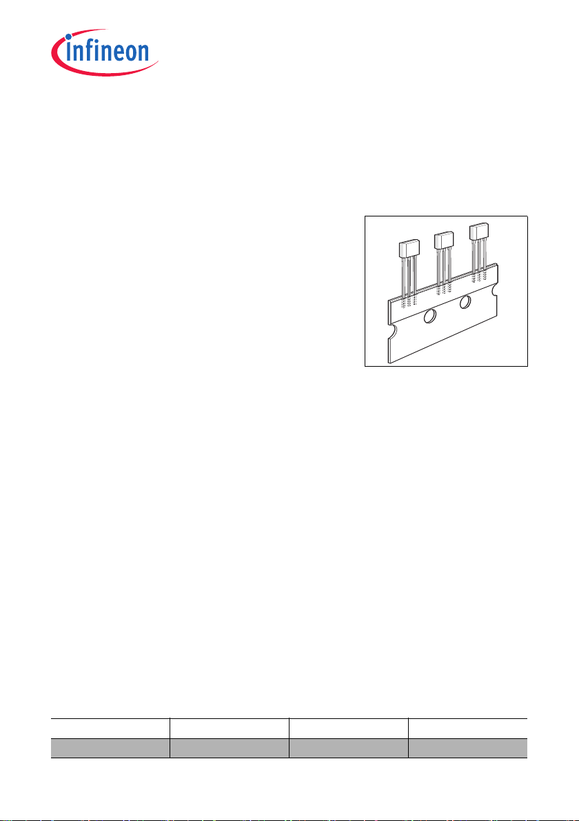
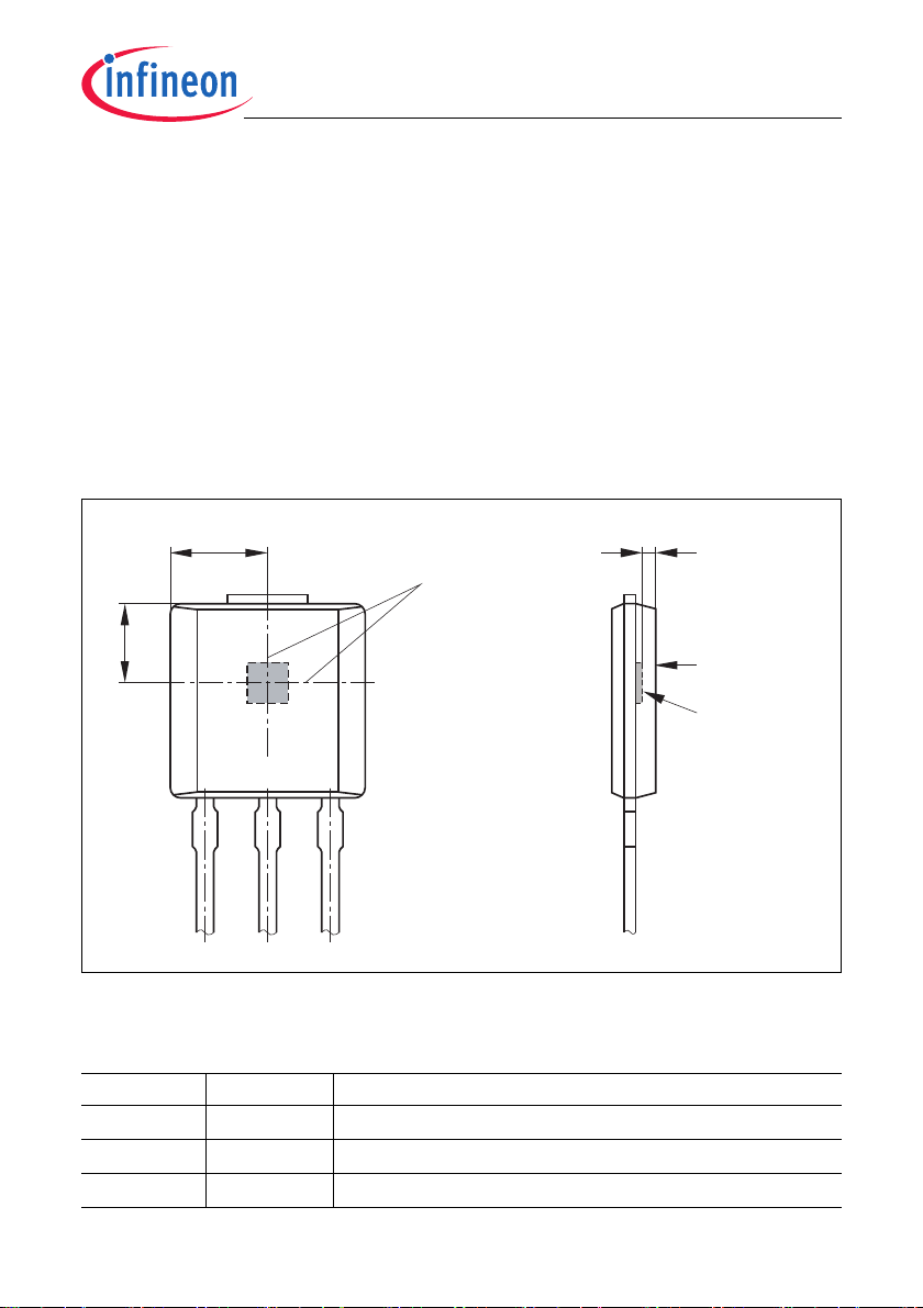
1.3 Pin Configuration
Figure 1 shows the location of the Hall element in the chip and the distance between the
Hall probe and the surface of the package.
Figure 1 Pin Configuration and Hall Cell Location
Table 1 Pin Definitions and Functions
Pin No. Symbol Function
1
2
3
Data Sheet 8 V 2.10, 2020-04
V
DD
GND
OUT
Supply voltage / programming interface
Ground
Output voltage / programming interface
Page 9
HALL
Bias
A
D
DSP
D
A
A
D
Temp.
Sense
ROM
EEPROM
Interface
enable
OUT
V
DD
GND
Supply
OBD
V
DD
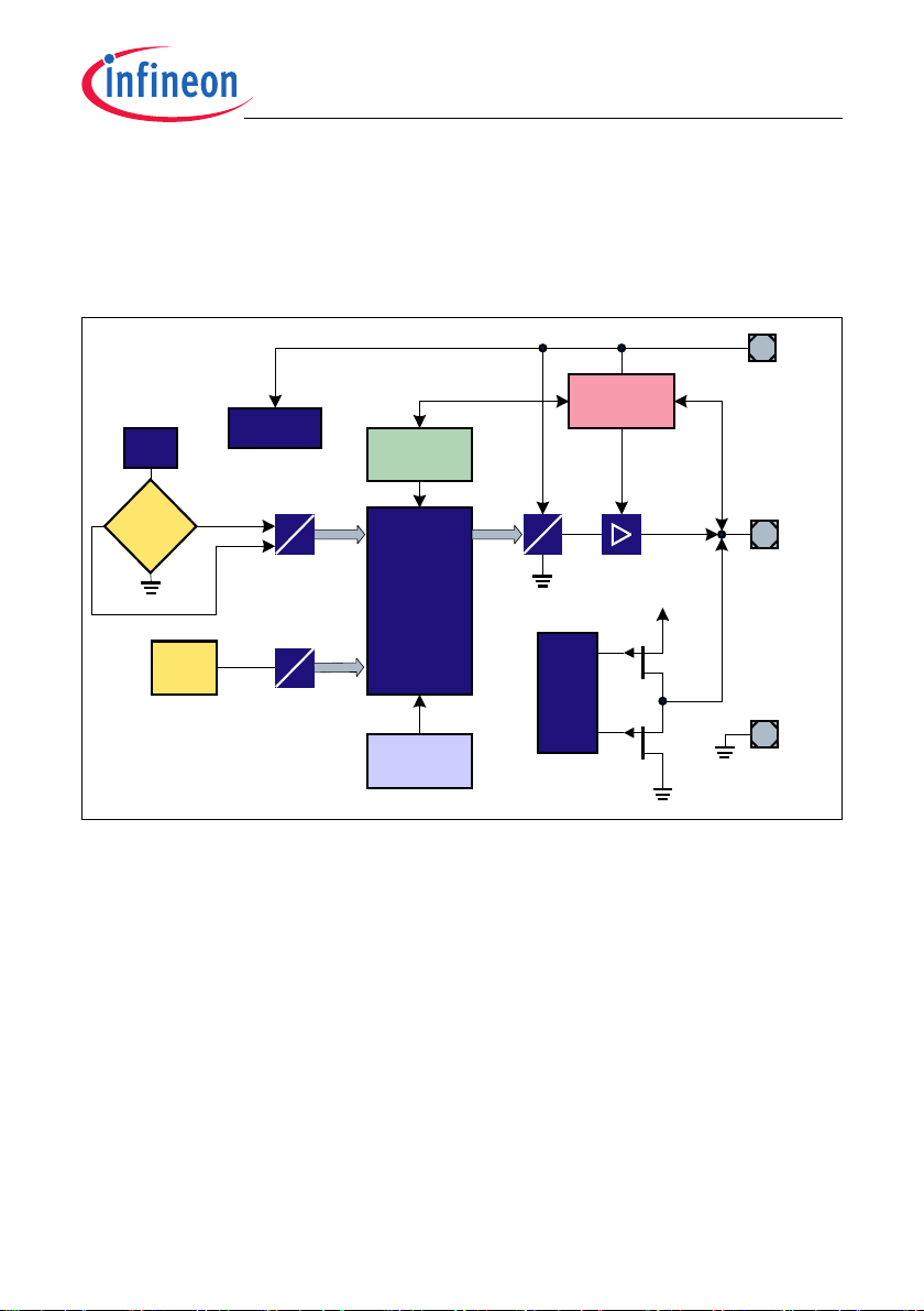
2 General
2.1 Block Diagram
Figure 2 shows a simplified block diagram.
TLE4997E2
General
Figure 2 Block Diagram
2.2 Functional Description
The linear Hall IC TLE4997E2has been designed specifically to meet the demands of
highly accurate rotation and position detection, as well as for current measurement
applications.
The sensor provides a ratiometric analog output voltage, which is ideally suited to
Analog-to-Digital (A/D) conversion with the supply voltage as a reference.
The IC is produced in BiCMOS technology with high voltage capability and also provides
reverse polarity protection.
Digital signal processing using a 16-bit DSP architecture and digital temperature
compensation guarantees excellent stability over a long period of time.
The minimum overall resolution is 12 bits. Nevertheless, some internal stages work with
resolutions up to 20 bits.
Data Sheet 9 V 2.10, 2020-04
Page 10

TLE4997E2
General
2.3 Principle of Operation
• A magnetic flux is measured by a Hall-effect cell.
• The output signal from the Hall-effect cell is converted from Analog to Digital signals.
• The chopped Hall-effect cell and continuous-time A to D conversion provide very low
and stable magnetic offset.
• A programmable Low-Pass filter reduces the noise.
• The temperature is measured and A to D converted.
• Temperature compensation is processed digitally using a second order function.
• Digital processing of output voltage is based on zero field and sensitivity value.
• The output voltage range can be clamped by digital limiters.
• The final output value is D to A converted.
• The output voltage is proportional to the supply voltage (ratiometric DAC).
V
• An On-Board-Diagnostics (OBD) circuit connects the output to
DD
or GND in case of errors.
2.4 Further Notes
Product qualification is based on “AEC Q100” (Automotive Electronics Council - Stress
test qualification for integrated circuits).
Data Sheet 10 V 2.10, 2020-04
Page 11
TLE4997E2
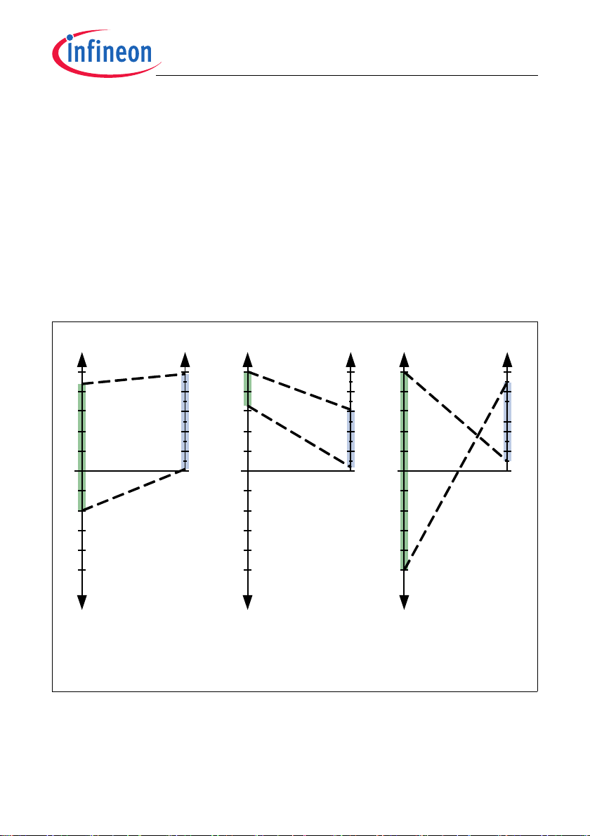
0
5
50
-50
5100
-100
5200
-200
V
OUT
(V)
V
OUT
V
OUT
00
B (mT)
V
OUT
(V)
B (mT)
V
OUT
(V)
B (mT)
000
Example 1:
- Bipolar
Example 2:
-Unipolar
-Big offset
- Outp ut for 3.3 V
Example 3:
- Bipolar
- Inverted (neg. gain)
General
2.5 Transfer Functions
The examples in Figure 3 show how easily different magnetic field ranges can be
mapped to the output voltage.
• Polarity Mode:
– Unipolar: Only North- or South-oriented magnetic fields are measured.
– Bipolar: Magnetic fields can be measured in both orientations.
The limit points must not be symmetric to the zero field point.
• Inversion: The gain values can be set positive or negative.
Figure 3 Examples of Operation
Note: Due to the ratiometry, voltage drops at the V
line are imaged in the output
DD
signal.
Data Sheet 11 V 2.10, 2020-04
Page 12

TLE4997E2
Maximum Ratings
3 Maximum Ratings
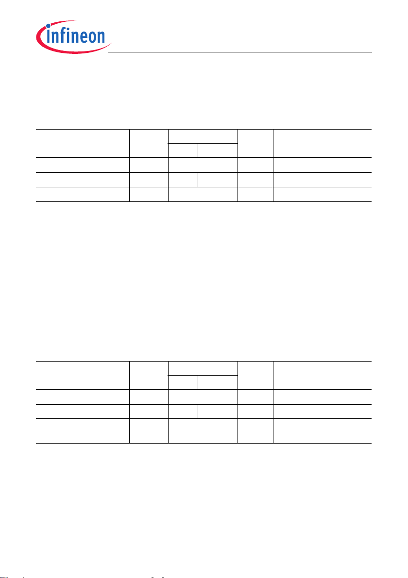
Table 2 Absolute Maximum Ratings
Parameter Symbol Limit Values Unit Notes
min. max.
SS
T
ST
T
J
V
DD
)
I
DDov
Storage temperature
Junction temperature
Voltage on VDD pins with
respect to ground (
V
Supply current
@ overvoltage
Supply current
I
DDrev
@ reverse voltage
Voltage on output pin with
V
OUTov
respect to ground (VSS)
Magnetic field B
ESD protection
1)
For limited time only. Depends on customer temperature lifetime cycles. Please ask for support by Infineon.
2)
max 24 h @ -50°C ≤ Ta< 30°C
max 10 min. @ 30°C ≤
max 30 sec. @ 80°C ≤
max 15 sec. @ 125°C ≤
3)
max. 24 h @ TJ< 80°C.
4)
Guaranteed by laboratory characterization, tested at ±18V.
5)
Max. 1 ms @ TJ< 30°C; -8.5 V for 100 h @ TJ< 80°C.
6)
100 pF and 1.5 kΩ
T
T
< 80°C
a
< 125°C
a
T
≤ 150°C.
a
V
MAX
ESD
-40 150 °C
R
THja
1)
≤ 150 K/W
-40 170 °C For 96h
-20
2)
20
3)
4)
V
-52mA
- 75 - mA
-16
5)
16
3)
V R
≤ 150 K/W
THja
may be > V
V
out
- unlimited T
- 4.0 kV According HBM
JESD22-A114-B
DD
6)
Note: Stresses above those listed under “Absolute Maximum Ratings” may cause
permanent damage to the device. This is a stress rating only and functional
operation of the device at these or any other conditions above those indicated in
the operational sections of this specification is not implied. Furthermore, only
single error cases are assumed. More than one stress/error case may also
damage the device.
Exposure to absolute maximum rating conditions for extended periods may affect
V
device reliability. During absolute maximum rating overload conditions (
> V
IN
DD
or VIN< VSS) the voltage on VDD pins with respect to ground (VSS) must not
exceed the values defined by the absolute maximum ratings.
Data Sheet 12 V 2.10, 2020-04
Page 13

TLE4997E2
Operating Range
4 Operating Range
The following operating conditions must not be exceeded in order to ensure correct
operation of the TLE4997E2. All parameters specified in the following sections of this
document refer to these operating conditions, unless otherwise indicated.
Table 3 Operating Range
Parameter Symbol Limit Values Unit Notes
min. max.
Supply voltage
Output current I
Load resistance R
Load capacitance C
Junction temperature
Useful lifetime
1)
For reduced output accuracy.
2)
For V
within the range of 5% ... 95% of VDD.
OUT
3)
R
≤ 150 K/W.
THja
4)
For reduced magnetic accuracy.
5)
Not additive.
V
DD
OUT
L
L
3)
T
J
t
Live
4.5 5.5 V
4 7 V Extended range
-1 1 mA
10
10
-
kΩ Pull-down to GND
-
2)
Pull-up to V
DD
0210nF
-40 125
150
°C For 5000h
For 1000h
4) 5)
- 16 years
1)
Note: Keeping signal levels within the limits specified in this table ensures operation
without overload conditions.
Data Sheet 13 V 2.10, 2020-04
Page 14

TLE4997E2
Electrical and Magnetic Parameters
5 Electrical and Magnetic Parameters
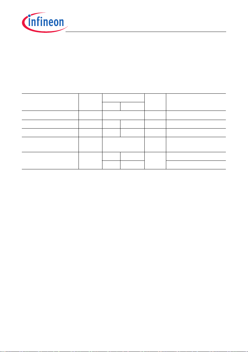
Table 4 Electrical Characteristics
Parameter Symbol Limit Values Unit Notes
min. typ. max.
Output voltage range
Supply current
Output current @ OUT
V
OUT
I
DD
I
OUTsh
shorted to supply lines
Zero field voltage
Zero field voltage drift
Ratiometry error E
Thermal resistance R
Power on time
Power On Reset level V
Output DAC quantization
V
ZERO
Δ
V
RAT
thJA
R
thJC
t
Pon
DDpon
Δ
V
Output DAC resolution - 12 bit
Output DAC bandwidth
Output noise V
Differential non-linearity
Signal delay
1)
Also in extended VDD range. For V
2)
Programmable in steps of 1.22 mV ( @ VDD=5V).
3)
For Sensitivity S ≤ 25 mV/mT. For higher sensitivities the magnetic offset drift is dominant. This means that for
the precalibrated (typical) 60mV/mT sensitivity the typical output drift might be given due to the allowed
magnetic offset tolerence up to ±0.4mT x 60 mV/mT = ±24 mV.
4)
For 4.5 V≤V
5)
For the maximum error in the extended voltage range, see “Ratiometry” on Page 15.
6)
More information, see “DAC Input Interpolation Filter” on Page 22.
7)
100 mT range, sensitivity 60 mV/mT, LP-filter 244 Hz, 160 Hz external RC low pass filter as application circuit.
8)
’5% exceeded’ means that 5 of 100 continuously measured V
9)
A sinusoidal magnetic field is applied, V
≤5.5 V and within nominal V
DD
f
DAC
noise
DNL
t
DS
5
-9594% of
6
V
37.510mA
For TA ≤ 120°C
For TA> 120°C
DD
1)
-30 - 30 mA For operating supply
voltage range only
-100 - 100 % Of V
-10 - 10 mV In lifetime
ZERO
DD
-10 - 10 mV Error band ov. temp.
-0.25 - +0.25 % Of V
DD
- - 219 K/W Junction to air
- - 47 K/W Junction to case
--110ms
Δ
V
OUT
Δ
V
OUT
2-4 V
OUT
1.22 mV @ VDD=5V
- 3.2 - kHz Interpolation filter
- - 4.68 mVpp5% exceeded
-1 - 1 LSB Of output DAC
- - 250 µs @ 100 Hz
within the range of 5%... 95% of VDD, I
OUT
range; see “Ratiometry” on Page 15 for details on E
OUT
samples are out of limit.
OUT
shows amplitude of 20% of VDD, no LP filter is selected.
OUT
OUT
= 0mA.
2)
3)
4)5)
≤ ±5% of V
≤ ±1% of V
7)8)
9)
6)
RAT
3)
DD
DD
.
Data Sheet 14 V 2.10, 2020-04
Page 15

TLE4997E2
E
RAT
V
OUTVDD
()
V
DD
-------------------------------
V
OUT
5V()
5V
---------------------------
–
èø
ç÷
æö
= 100× %
E
RAT
%
0
V
DD
V
4567
0.25
0.5
0.75
1
-0.25
-0.5
-0.75
-1
Electrical and Magnetic Parameters
Ratiometry
The linear Hall sensor works like a potentiometer. The output voltage is proportional to
the supply voltage. The division factor depends on the magnetic field strength. This
behavior is called “ratiometric”’.
V
The supply voltage
microcontroller. In this case, variations of VDD are compensated.
The ratiometry error is defined as follows:
The ratiometry error band displays as a “Butterfly Curve”.
should be used as the reference for the A/D Converter of the
DD
Figure 4 Ratiometry Error Band
Note: Take care of possible voltage drops on the VDD and V
result. Ideally, both values are acquired and their ratio is calculated to gain the
highest accuracy. This method should be used especially during calibration.
Data Sheet 15 V 2.10, 2020-04
line degrading the
OUT
Page 16

Electrical and Magnetic Parameters
Calculation of the Junction Temperature
The total power dissipation P
temperature. The power multiplied with the total thermal resistance R
Ambient) leads to the final junction temperature. R
values of the two components
R
thJA
T
= TA +
J
Δ
T = R
= R
thJA
thJC
Δ
T
xP
+ R
TOT
thCA
=R
thJA
of the chip increases its temperature above the ambient
TOT
is the sum of the addition of the
thJA
thJA
Junction to Case and Case to Ambient.
x(VDDx IDD+ V
OUT
x I
OUT
) I
, I
> 0, if direction is into IC
DD
OUT
Example (assuming no noticeable load on Vout):
–
V
= 5 V
DD
– I
= 10 mA
DD
Δ
T = 219 [K/W] x (5 [V] x 0.01 [A] + 0 [VA]) = 11 K
–
For moulded sensors, the calculation with R
is more adequate.
thJC
Magnetic Parameters
Table 5 Magnetic Characteristics
Parameter Symbol Limit Values Unit Notes
min. typ. max.
Sensitivity
Magnetic field range
Integral nonlinearity
Magnetic offset B
S
MFR
INL
OS
Magnetic offset drift ΔB
1)
Programmable in steps of 0.024%, @ V
2)
This range is also used for temperature and offset pre-calibration of the IC.
3)
Depending on the Offset and Gain settings, the output may saturate at lower fields.
4)
INL = V
V
5)
In operating temperature range and over lifetime.
6)
For Sensitivity S > 25 mV / mT. For lower sensitivities, the zero field voltage drift is dominant.
7)
Measured at ± 100 mT range.
- V
out,lse
with V
out
) for TJ≤ 120°C and (6% of VDD)<V
DD
= least square error fit of V
out,lse
± 12.5 - ± 300 mV/mT1)
± 50 ± 100
2)
± 200 mT Programmable
-15 - 15 mV = ± 0.3% of V
-400 - 400 μT
- 5 - 5 μT / °C Error band
OS
= 5 V and TJ=25°C
DD
. Valid in the range (5% of VDD)<V
< (94% of VDD) for 120°C < TJ ≤ 150°C
OUT
out
5) 6) 7)
TLE4997E2
(Junction to
3)
4)
DD
7)
< (95% of
OUT
Data Sheet 16 V 2.10, 2020-04
Page 17

D
A
A
D
X
Stored in
EEPROM
Memory
X
-T
0
+
TC
1
X
A
D
Temperature
Compensation
Hall
Sensor
Temperature
Sensor
Limiter
(Clamp)
out
1
X
Range LP
LP
DAC
+
Offset
Gain
X
TC
2
+
6 Signal Processing
The flow diagram in Figure 5 shows the data processing algorithm.
TLE4997E2
Signal Processing
Figure 5 Signal Processing Flow
Magnetic Field Path
• The analog output signal of the chopped Hall cell is converted in the continuous-time
A/D Converter. The range of the chopped A/D Converter can bet set in several steps
(see Table 6). This assures a suitable level for the A/D Converter.
• After the A/D conversion, a digital low pass filter reduces the bandwidth (Table 10).
• A multiplier amplifies the value according to the gain setting (see Table 8) plus
temperature compensation.
• The offset value is added (see Table 9).
• A limiter reduces the resulting signal to 12 bits and feeds the D/A converter.
Temperature Compensation
(Details are listed in Chapter 8)
• The output signal of the temperature cell is also A/D converted.
• The temperature is normalized by subtraction of the T
• The linear path is multiplied with the TC
Data Sheet 17 V 2.10, 2020-04
quadratic function).
value.
1
value (zero point of the
0
Page 18

TLE4997E2
Signal Processing
• In the quadratic path, the difference temperature is squared and multiplied with the
TC2 value.
• Both path outputs are added together to the gain value from the EEPROM.
6.1 Magnetic Field Ranges
The working range of the magnetic field defines the input range of the A/D Converter. It
is always symmetric to the zero field point. Any two points in the magnetic range can be
selected to be the end points of the output curve. The output voltage represents the
range between the two points.
In the case of fields higher than the range values, the output signal may be distorted.
The range must be set before the calibration of offset and gain.
Table 6 Range Setting
Range Range in mT Parameter R
Low ± 50 3
Mid ± 100 1
High ± 200 0
Table 7 Range
Parameter Symbol Limit Values Unit Notes
min. max.
Register size
1)
Ranges do not have a guaranteed absolute accuracy. The temperature pre-calibration is performed in the mid
range (100 mT).
Data Sheet 18 V 2.10, 2020-04
R
2bit
1)
Page 19
TLE4997E2
Gain
G 16384–()
4096
------------------------------
=
V
OS
OS 16384–()
4096
---------------------------------
V
DD
×=
Signal Processing
6.2 Gain Setting
The sensitivity is defined by the range and the gain setting. The output of the A/D
Converter is multiplied with the gain value.
Table 8 Gain
Parameter Symbol Limit Values Unit Notes
min. max.
Register size
Gain range
G
Gain
Gain quantization steps ΔGain 244.14 ppm Corresponds to 1/4096
1)
For gain values between - 0.5 and + 0.5, the numeric accuracy decreases.
To obtain a flatter output curve, it is recommended to select a higher range setting.
2)
A gain value of +1.0 corresponds to a typical 40 mV/mT sensitivity (100 mT range, not guaranteed). Infineon
pre-calibrates the samples to 60mV/mT (100mT range) in the final test, but does not guarantee the accuracy
of this calibration. It is crucial to do a final calibration of each IC within the application using the Gain/V
The gain value can be calculated by
:
15 bit Unsigned integer value
- 4.0 3.9998 -
1)2)
OS
value.
6.3 Offset Setting
The offset voltage corresponds to an output voltage with zero field at the sensor.
Table 9 Offset
Parameter Symbol Limit Values Unit Notes
min. max.
Register size
Offset range
Offset quantization
OS
V
ΔV
OS
OS
steps
1)
Infineon pre-calibrates the samples at zero field to 50% of VDD (100mT range) in the final test, but does not
guarantee the accuracy of this calibration. It is crucial to do a final calibration of each IC within the application
using the Gain/V
OS
value.
The offset value can be calculated by:
Data Sheet 19 V 2.10, 2020-04
15 bit Unsigned integer value
-400 399 % V
DD
1)
1.22 mV @ VDD=5V
generally V
DD
/ 4095
Page 20

TLE4997E2
Signal Processing
6.4 DSP Input Low Pass Filter
A digital Low Pass Filter is placed between the Hall A/D Converter and the DSP to
reduce the noise level. The Low Pass filter has a constant DC amplification of 0 dB (this
is exactly a gain of 1), which means that its setting has no influence on the internal Hall
A/D Converter value.
The bandwidth can be set in 8 steps.
Table 10 Low Pass Filter Setting
Parameter LP Cutoff frequency in Hz (at 3dB attenuation)
078
1244
2421
3615
4826
51060
61320
7 off
1)
As this is a digital filter running with an RC-based oscillator, the cutoff frequency may vary within ±25%.
2)
The output low pass-interpolation filter behavior remains as main component in the signal path.
2)
1)
Table 11 Low Pass Filter
Parameter Symbol Limit Values Unit Notes
min. max.
Register size
Corner frequency
LP
Δ
f -25 +25 %
3bit
variation
Note: In Low Pass filter setting 7 (filter off), the output noise increases. Because of
higher DSP load, the current consumption also rises slightly.
Data Sheet 20 V 2.10, 2020-04
Page 21

TLE4997E2
10
1
10
2
10
3
0
-6
-5
-4
-3
-2
-1
Magnitude (dB)
Frequency (Hz)
Signal Processing
Figure 6 shows the characteristic of the filter as a magnitude plot (the highest setting is
marked). The “off” position would be a flat 0 dB line. In this case, the output decimation
filter limits the bandwidth of the sensor. The update rate after the Low Pass filter is
16 kHz.
Figure 6 DSP Input Filter (Magnitude Plot)
Data Sheet 21 V 2.10, 2020-04
Page 22
TLE4997E2
10
1
10
2
10
3
0
-6
-5
-4
-3
-2
-1
Magnitude (dB)
Frequency (Hz)
10
4
Signal Processing
6.5 DAC Input Interpolation Filter
An interpolation filter is placed between the DSP and the output DAC. It cannot be
switched off. This filter limits the frequency behavior of the complete system if the DSP
input filter is disabled. The update rate after the interpolation filter is 256 kHz.
Figure 7 DAC Input Filter (Magnitude Plot)
Note: As this is a digital filter running with an RC-based oscillator, the cutoff frequency
may vary within ±25%.
Data Sheet 22 V 2.10, 2020-04
Page 23
TLE4997E2
V
CLL
CL
4096
------------
V
DD
×=
V
CLH
CH
4096
------------
V
DD
×=
Signal Processing
6.6 Clamping
The clamping function is useful for splitting the output voltage into the operating range
and error ranges. If the magnetic field is outside the selected measurement range, the
V
output voltage
Table 12 Clamping
Parameter Symbol Limit Values Unit Notes
Register size
Clamping voltage low
Clamping voltage high V
Clamping quantization
steps
Clamping voltage drift
1)
If clamping is set, it must be within the allowed output voltage range to be effective.
2)
Valid in the range (5% of VDD)<V
and (6% of
V
is limited to the clamping values.
out
min. max.
CL,CH
DD
V
CLL
CLH
Δ
V
Δ
V
)<V
< (94% of VDD) for 120°C < TJ ≤ 150°C
OUT
0 99.98 % V
0 99.98 % V
CLQ
-15 15 mV in lifetime
CL
-15 15 over temperature
< (95% of VDD) for TJ≤ 120°C
OUT
2 x 12 bit
1)
DD
1)
DD
1.22 mV @ VDD=5V
2)
2)
The clamping values are calculated by:
Clamping low voltage:
Clamping high voltage:
Note: For an exact setup, the register value may be re-adjusted due to the actual output
voltage in the clamping condition. The output voltage range itself has electrical
limits. See the Electrical Characteristics of
Data Sheet 23 V 2.10, 2020-04
V
.
out
Page 24
TLE4997E2
0
1
B
min
B (mT)
B
max
V
out
(V)
5
2
4
3
Error range
Error range
Operating range
V
CLH
V
CLL
Signal Processing
Figure 8 shows an example in which the magnetic field range between B
is mapped to voltages between 0.8 V and 4.2 V.
If it is not necessary to signal errors, the maximum output voltage range between 0.3 V
and 4.7 V can be used.
min
and B
max
Figure 8 Clamping Example
Note: The high value must be above the low value.
If V
is set to a higher value than V
CLL
lead to a constant output voltage independent of the magnetic field strength.
CLH
, the V
value is dominating. This would
CLH
Data Sheet 24 V 2.10, 2020-04
Page 25
TLE4997E2
Error Detection
7 Error Detection
Different error cases can be detected by the On-Board-Diagnostics (OBD) and reported
to the microcontroller. The OBD is useful only when the clamping function is enabled. It
is important to set the clamping threshold values inside the error voltage values shown
in Table 13 and Table 14 to ensure that it is possible to distinguish between correct
output voltages and error signals.
7.1 Voltages Outside the Operating Range
The output signals error conditions, if VDD lies
• inside the ratings specified in Table 2 "Absolute Maximum Ratings" on Page 12
• outside the range specified in Table 3 "Operating Range" on Page 13.
Table 13 Undervoltage and Overvoltage (All values with RL ≥ 10k)
Parameter Symbol Limit Values Unit Notes
min. max.
Undervoltage threshold
Overvoltage threshold
Output voltage
@ undervoltage
Output voltage
@ overvoltage
Supply current
1)
For overvoltage and reverse voltage, see Table 2 "Absolute Maximum Ratings" on Page 12.
1)
V
DDuv
V
DDov
V
OUTuv
V
OUTov
I
DDuv
34V
78.3V
0.95 x VDD-V3V ≤ VDD≤ V
0.97 x VDD-VV
DDov
DDuv
< VDD≤ 16 V
- 10 mA @ undervoltage
7.2 Open Circuit of Supply Lines
In the case of interrupted supply lines, the data acquisition device can alert the user. If
two sensors are placed in parallel, the output of the remaining working sensor may be
still used for an emergency operation.
Table 14 Open Circuit (OBD Parameters)
Parameter Symbol Limit Values Unit Notes
min. max.
Output voltage
@ open V
DD
line
Output voltage
@ open
1)
Data Sheet 25 V 2.10, 2020-04
GND line
With VDD= 5 V and R
V
V
OUT
OUT
00.18
4.82
4.8
≥ 10 kΩ pull-down or RL≥ 20 kΩ pull-up.
L
1)
VT
0.2
5VT
≤120°C
J
120°C < TJ ≤ 150°C
≤120°C
J
120°C < TJ ≤ 150°C
Page 26

TLE4997E2
Error Detection
7.3 Not Correctable EEPROM Errors
The parity method is able to correct one single bit in one EEPROM line. One other single
bit error in another line can also be detected. As this situation is not correctable, this
V
status is signalled at the output pin by clamping the output value to
Table 15 EEPROM Error Signalling
Parameter Symbol Limit Values Unit Notes
min. max.
Output voltage @
V
OUT
0.97 x V
DDVDD
V
EEPROM error
DD
.
Data Sheet 26 V 2.10, 2020-04
Page 27

TLE4997E2
S
TC
T() 1 TC
1
TT
0
–()× TC
2
TT
0
–()
2
×++=
Temperature Compensation
8 Temperature Compensation
The magnetic field strength of a magnet depends on the temperature. This material
constant is specific to different magnet types. Therefore, the TLE4997E2 offers a second
order temperature compensation polynomial, by which the Hall signal output is multiplied
in the DSP. There are three parameters for the compensation:
• Reference temperature T
• A linear part (1st order) TC
• A quadratic part (2nd order) TC
The following formula describes the sensitivity dependent on the temperature in relation
to the sensitivity at the reference temperature T0:
For more information, see also the signal processing flow in Figure 5.
The full temperature compensation of the complete system is done in two steps:
1. Pre-calibration in the Infineon final test.
The parameters TC1, TC2, T0 are set to maximally flat temperature characteristics
regarding the Hall probe and internal analog processing parts.
2. Overall System calibration.
The typical coefficients TC1, TC2, T0 of the magnetic circuitry are programmed. This
can be done deterministically, as the algorithm of the DSP is fully reproducible. The
final settings of the TC1, TC2, T0 values are relative to the pre-calibrated values.
Table 16 Temperature Compensation
Parameter Symbol Limit Values Unit Notes
Register size
st
order coefficient TC
1
TC
1
Quantization steps of TC
Register size
nd
order coefficient TC
2
TC
2
Quantization steps of TC
Register size
T
0
Reference temperature
Quantization steps of
1)
Full adjustable range: -2441 to +5355 ppm/°C, can be only used after confirmation by Infineon
2)
Full adjustable range: -15 to +15 ppm/°C², can be only used after confirmation by Infineon
3)
A quantization step of 1°C is handled by algorithm (See Application Note).
0
1
2
min. max.
TL
TC
1
Δ
TC
1
TQ
TC
2
Δ
TC
2
TR
T
0
T
Δ
T
0
- 9 bit Unsigned integer values
-1000 2500 ppm/ °C1)
1
1
15.26 ppm/ °C
- 8 bit Unsigned integer values
- 4 4 ppm/ °C²2)
2
2
0.119 ppm/ °C²
- 3 bit Unsigned integer values
-48 64 °C
0
16 °C
3)
Data Sheet 27 V 2.10, 2020-04
Page 28

TC
1
TL 160–
65536
----------------------
1000000×=
TC
2
TQ 128–
8388608
-----------------------
1000000×=
T
0
16T R 48–=
V
OUT
B
IN
B
FSR
-------------
S
TC
× S
TCHall
× S
o
V
DD
××
èø
ç÷
æö
V
OS
+=
S
TC
TJT0–()S
TCHall
TJ()× 1≈
B
IN
T()
B
IN
T0()
--------------------
S
TCnew
T() S
TCHall
T()×× STCT() S
TCHall
T()× 1≈≈
B
IN
T()
B
IN
T0()
--------------------
S
TCnew
T()× STCT()≈
8.1 Parameter Calculation
The parameters TC1, TC2 and T0 may be calculated by:
TLE4997E2
Temperature Compensation
Now the output V
for a given field BIN at a specific temperature can be roughly
OUT
calculated by:
is the full range magnetic field. It is dependent on the range setting (e.g 100 mT).
B
FSR
S
is the nominal sensitivity of the Hall probe times the Gain factor set in the EEPROM.
o
STC is the temperature-dependent sensitivity factor calculated by the DSP.
S
is the temperature behavior of the Hall probe.
TCHall
The pre-calibration at Infineon is performed such that the following condition is met:
Within the application, an additional factor BIN(T) / BIN(T0) will be given due to the
magnetic system. STC needs now to be modified to S
so that the following condition
TCnew
is satisfied:
S
Therefore, the new sensitivity parameters
pre-calibrated setup S
using the relation:
TC
can be calculated from the
TCnew
Data Sheet 28 V 2.10, 2020-04
Page 29

TLE4997E2
Calibration
9Calibration
A special hardware interface to an external computing system and measurement
equipment is required for calibration of the sensor. All calibration and setup bits can be
written into a random access memory (RAM). This allows the EEPROM to remain
untouched during the entire calibration process. Therefore, this temporary setup (using
the RAM only) does not stress the EEPROM—and even allows a pre-verification
setup before programming—as the number of EEPROM programming cycles is limited
to provide a high data endurance.
The digital signal processing is completely deterministic. This allows a two point
calibration in one step without iterations. The two magnetic fields (here described as two
“positions” of an external magnetic circuitry) need to be applied only once. Furthermore,
a complete setup and calibration procedure can be performed requiring only one
EEPROM programming cycle at the end
2)
.
After setting up the temperature coefficients, the calibrated Hall A/D Converter values of
both positions need to be read and the sensor output signals (using a DAC test mode)
need to be acquired for the corresponding end points. Using this data, the signal
processing parameters can be immediately calculated with a program running on the
external computing system.
Note: The calibration and programming process must be performed only at the
start of life of the device.
Table 17 Calibration Characteristics
Parameter Symbol Limit Values Unit Notes
min. max.
Temperature of sensor at
t
CAL
10 30 °C
2 point calibration and
programming
2 point calibration
accuracy
1)
1)
Setup and validation performed at start of life.
Δ
V
Δ
V
-10 10 mV Position 1
CAL1
-10 10 mV Position 2
CAL2
1)
of the
Note: Depending on the application and external instrumentation setup, the accuracy of
the 2 point calibration can be improved.
1)
This feature is not required for a deterministic two-point setup to fulfill the specification.
2)
Details and basic algorithms for this step are available on request.
Data Sheet 29 V 2.10, 2020-04
Page 30

TLE4997E2
User-Calibration Bits
Pre-Calibration Bits
Column Parity Bi ts
RowA Parity Bits
Calibration
9.1 Calibration Data Memory
When the MEMLOCK bits are programmed (two redundant bits), the memory contents
are frozen and may no longer be changed. Furthermore, the programming interface is
locked out and the chip remains in Application Mode only. This prevents accidental
programming due to environmental influences.
Figure 9 EEPROM Map
A matrix parity architecture allows the automatic correction of any single bit error. Each
row is protected by a row parity bit. The sum of bits set including this bit must be an odd
number (ODD PARITY). Each column is additionally protected by a column parity bit.
The sum of all the bits in the even positions (0, 2, etc.) of all lines must be an even
number (EVEN PARITY); the sum of all the bits in the odd positions (1,3, etc.) must be
an odd number (ODD PARITY). This mechanism of different parity calculations protects
against many block errors (such as erasing a full line or even the entire EEPROM).
When modifying the application bits (such as Gain, Offset, TC, etc.) the parity bits must
be updated. For the column bits, the pre-calibration area must be also read out and
considered for correct parity generation.
Note: A specific programming algorithm must be followed to ensure the data retention.
A separate detailed programming specification is available on request.
Data Sheet 30 V 2.10, 2020-04
Page 31

TLE4997E2
Calibration
Table 18 Programming Characteristics
Parameter Symbol Limit Values Unit Notes
min. max.
Number of EEPROM
programming cycles
Ambient temperature at
N
T
PRG
PRG
- 10 Cycles
1)
10 30 °C
Programming allowed
only at start of lifetime
programming
Programming time
Calibration memory
Error correction
1)
1 cycle is the simultaneous change of ≥ 1bit.
2)
Depending on clock frequency at VDD, write pulse 10ms ±1%, erase pulse 80ms ±1%.
t
PRG
-
-
100 - ms For complete memory
135 Bit All active EEPROM bits
25 Bit All parity EEPROM bits
2)
9.2 Programming Interface
The supply pin and the output pin are used as two-wire interface to transmit the
EEPROM data to and from the sensor.
This allows
• communication with high data reliability
• bus-type connection of several sensors
In many applications, two sensors are used to measure the same parameter. This
redundancy allows the operation to continue in an emergency mode. If both sensors use
the same power supply lines, they can be programmed together in parallel.
The data transfer protocol and programming is described in a separate document
(TLE4997 Programming Guide).
9.3 Laboratory Evaluation Programmer
For the programming of evaluation samples and QA (quality assurance) samples a
programming equipment is available on request.
Data Sheet 31 V 2.10, 2020-04
Page 32

Application Circuit
optional
Volt age Tr acker
e.g .
TLE4250
Ref
ADC
ref
ADC
in1
ADC
in2
ADC
GND
47nF
10k
100 nF10k100 nF47nF
47nF
10k
100 nF10k100 nF47nF
µC
TLE
4997
out
V
DD
GND
TLE
4997
out
V
DD
GND
10 Application Circuit
Figure 10 shows the connection of multiple sensors to a microcontroller.
TLE4997E2
Figure 10 Application Circuit
Note: For calibration and programming, the interface must be connected directly to the
output pin.
The given application circuit must be regarded as only an example. It needs to be
adapted according to the requirements of the specific application.
Data Sheet 32 V 2.10, 2020-04
Page 33

1) No solder function area
Molded body dimensions do not unclude plastic or metal protrusion of 0.15 max per side
±0.3
12.7
±0.4
6.35
12.7
±1
Total tolerance at 19 pitches ±1
±0.3
4
19
±0.5
9
-0.50
+0.75
33 MAX.
(Useable
Length)
(10)
±0.5
18
A
±0.5
6
1
-1
-0.15
0.25
±0.1
0.39
Ta pe
Adhesive
Ta pe
(0.25)
1
±0.2
1)
0.1 MAX.
0.5
0.5
±0.05
±0.1
0.42
3x
1.5
±0.05
4.06
4.05
±0.05
2 x 1.27 = 2.54
A
2
±0.05
1.5
0.36
±0.05
0.82
±0.05
P-PG-SSO-3-10-PO V02
45˚
5˚
123
B
B
C2
C
11 Package Outlines
TLE4997E2
Package Outlines
Figure 11 PG-SSO-3-10 (Plastic Green Single Small Outline Package)
Data Sheet 33 V 2.10, 2020-04
Page 34

www.infineon.com
Published by Infineon Technologies AG
 Loading...