

Page 1

TLE4997
Configuration and Calibration of Linear Hall Sensor
User’s Manual
v01_01, 2019-08
Sense & Control
Page 2

Edition 2019-08
Published by
Infineon Technologies AG
81726 Munich, Germany
© 2019 Infineon Technologies AG
All Rights Reserved.
Legal Disclaimer
The information given in this document shall in no event be regarded as a guarantee of conditions or
characteristics. With respect to any examples or hints given herein, any typical values stated herein and/or any
information regarding the application of the device, Infineon Technologies hereby disclaims any and all warranties
and liabilities of any kind, including without limitation, warranties of non-infringement of intellectual property rights
of any third party.
Information
For further information on technology, delivery terms and conditions and prices, please contact the nearest
Infineon Technologies Office (www.infineon.com).
Warnings
Due to technical requirements, components may contain dangerous substances. For information on the types in
question, please contact the nearest Infineon Technologies Office.
Infineon Technologies components may be used in life-support devices or systems only with the express written
approval of Infineon Technologies, if a failure of such components can reasonably be expected to cause the failure
of that life-support device or system or to affect the safety or effectiveness of that device or system. Life support
devices or systems are intended to be implanted in the human body or to support and/or maintain and sustain
and/or protect human life. If they fail, it is reasonable to assume that the health of the user or other persons may
be endangered.
Page 3

TLE4997
User’s Manual
Table of Contents
Table of Contents
Table of Contents . . . . . . . . . . . . . . . . . . . . . . . . . . . . . . . . . . . . . . . . . . . . . . . . . . . . . . . . . . . . . . . . 3
1Scope . . . . . . . . . . . . . . . . . . . . . . . . . . . . . . . . . . . . . . . . . . . . . . . . . . . . . . . . . . . . . . . . . . . . . . . . . . 4
2 TLE4997 Signal Processing . . . . . . . . . . . . . . . . . . . . . . . . . . . . . . . . . . . . . . . . . . . . . . . . . . . . . . . . 4
3 TLE4997 Programming . . . . . . . . . . . . . . . . . . . . . . . . . . . . . . . . . . . . . . . . . . . . . . . . . . . . . . . . . . . . 5
3.1 Programmer Connection . . . . . . . . . . . . . . . . . . . . . . . . . . . . . . . . . . . . . . . . . . . . . . . . . . . . . . . . . . . . 5
3.2 Programming Interface . . . . . . . . . . . . . . . . . . . . . . . . . . . . . . . . . . . . . . . . . . . . . . . . . . . . . . . . . . . . . 6
3.2.1 Communication Scheme . . . . . . . . . . . . . . . . . . . . . . . . . . . . . . . . . . . . . . . . . . . . . . . . . . . . . . . . . . 6
3.3 Command Frame . . . . . . . . . . . . . . . . . . . . . . . . . . . . . . . . . . . . . . . . . . . . . . . . . . . . . . . . . . . . . . . . . 7
3.3.1 Data Frame . . . . . . . . . . . . . . . . . . . . . . . . . . . . . . . . . . . . . . . . . . . . . . . . . . . . . . . . . . . . . . . . . . . . 8
3.3.2 Interface Specification . . . . . . . . . . . . . . . . . . . . . . . . . . . . . . . . . . . . . . . . . . . . . . . . . . . . . . . . . . . . 8
3.4 Register Map . . . . . . . . . . . . . . . . . . . . . . . . . . . . . . . . . . . . . . . . . . . . . . . . . . . . . . . . . . . . . . . . . . . 11
3.5 EEPROM Map . . . . . . . . . . . . . . . . . . . . . . . . . . . . . . . . . . . . . . . . . . . . . . . . . . . . . . . . . . . . . . . . . . 13
3.6 Programming Flow . . . . . . . . . . . . . . . . . . . . . . . . . . . . . . . . . . . . . . . . . . . . . . . . . . . . . . . . . . . . . . . 14
3.6.1 Setting the TEST register . . . . . . . . . . . . . . . . . . . . . . . . . . . . . . . . . . . . . . . . . . . . . . . . . . . . . . . . 16
3.6.2 Readout of the EEPROM Content . . . . . . . . . . . . . . . . . . . . . . . . . . . . . . . . . . . . . . . . . . . . . . . . . . 16
3.6.3 Setting the EEPROM Content . . . . . . . . . . . . . . . . . . . . . . . . . . . . . . . . . . . . . . . . . . . . . . . . . . . . . 16
3.6.4 Calculation of Bits to Erase . . . . . . . . . . . . . . . . . . . . . . . . . . . . . . . . . . . . . . . . . . . . . . . . . . . . . . . 16
3.6.5 Calculation of Bits to Write . . . . . . . . . . . . . . . . . . . . . . . . . . . . . . . . . . . . . . . . . . . . . . . . . . . . . . . . 16
3.6.6 Margin Voltage Check . . . . . . . . . . . . . . . . . . . . . . . . . . . . . . . . . . . . . . . . . . . . . . . . . . . . . . . . . . . 17
3.6.7 DATA access example . . . . . . . . . . . . . . . . . . . . . . . . . . . . . . . . . . . . . . . . . . . . . . . . . . . . . . . . . . 17
3.6.8 Temporary overwrite of EEPROM data . . . . . . . . . . . . . . . . . . . . . . . . . . . . . . . . . . . . . . . . . . . . . . 18
3.6.9 DAC setup example . . . . . . . . . . . . . . . . . . . . . . . . . . . . . . . . . . . . . . . . . . . . . . . . . . . . . . . . . . . . . 19
4 Configuration & Calibration Parameters . . . . . . . . . . . . . . . . . . . . . . . . . . . . . . . . . . . . . . . . . . . . 20
4.1 Magnetic Field Range - R . . . . . . . . . . . . . . . . . . . . . . . . . . . . . . . . . . . . . . . . . . . . . . . . . . . . . . . . . . 20
4.2 Gain Setting - G . . . . . . . . . . . . . . . . . . . . . . . . . . . . . . . . . . . . . . . . . . . . . . . . . . . . . . . . . . . . . . . . . 20
4.3 Offset Setting - OS . . . . . . . . . . . . . . . . . . . . . . . . . . . . . . . . . . . . . . . . . . . . . . . . . . . . . . . . . . . . . . . 20
4.4 Low-Pass Filter - LP . . . . . . . . . . . . . . . . . . . . . . . . . . . . . . . . . . . . . . . . . . . . . . . . . . . . . . . . . . . . . . 21
4.5 DAC Input Interpolation Filter . . . . . . . . . . . . . . . . . . . . . . . . . . . . . . . . . . . . . . . . . . . . . . . . . . . . . . . 22
4.6 Clamping - CH, CL . . . . . . . . . . . . . . . . . . . . . . . . . . . . . . . . . . . . . . . . . . . . . . . . . . . . . . . . . . . . . . . 23
4.7 Temperature Compensation - TL, TQ & TT . . . . . . . . . . . . . . . . . . . . . . . . . . . . . . . . . . . . . . . . . . . . 24
5 Calibration of TLE4997 Temperature Compensation . . . . . . . . . . . . . . . . . . . . . . . . . . . . . . . . . . 25
5.1 Integrated Temperature Polynomial . . . . . . . . . . . . . . . . . . . . . . . . . . . . . . . . . . . . . . . . . . . . . . . . . . 25
5.2 Application Sensitivity Polynomial . . . . . . . . . . . . . . . . . . . . . . . . . . . . . . . . . . . . . . . . . . . . . . . . . . . 25
5.3 Determination of Sensitivity Polynomial from Measurement . . . . . . . . . . . . . . . . . . . . . . . . . . . . . . . 27
5.4 Calculation of Final Temperature Compensation Parameters . . . . . . . . . . . . . . . . . . . . . . . . . . . . . . 28
5.4.1 Algorithm for Finding the Optimum Temperature Coefficient Set . . . . . . . . . . . . . . . . . . . . . . . . . . 28
5.4.2 Example Implementation Code for Temperature Calibration . . . . . . . . . . . . . . . . . . . . . . . . . . . . . . 29
5.5 Usage of Infineon’s Temperature Calibration Tool . . . . . . . . . . . . . . . . . . . . . . . . . . . . . . . . . . . . . . . 32
6 Calibration of TLE4997 Output Characteristic . . . . . . . . . . . . . . . . . . . . . . . . . . . . . . . . . . . . . . . . 34
6.1 Two-Point Calibration Procedure . . . . . . . . . . . . . . . . . . . . . . . . . . . . . . . . . . . . . . . . . . . . . . . . . . . . 34
6.2 Two-Point Calibration Examples . . . . . . . . . . . . . . . . . . . . . . . . . . . . . . . . . . . . . . . . . . . . . . . . . . . . . 35
6.2.1 Calibration with Application Readout . . . . . . . . . . . . . . . . . . . . . . . . . . . . . . . . . . . . . . . . . . . . . . . . 35
6.2.2 Calibration without Application Readout . . . . . . . . . . . . . . . . . . . . . . . . . . . . . . . . . . . . . . . . . . . . . 36
User’s Manual 3 v01_01, 2019-08
Page 4

TLE4997
Stored in
EEPROM
Memory
+
A
D
Hall
Sensor
Limiter
(Clamp)
Out
X
Range LP
Offset
Gain
x
Clamping Low
Clamping High
A
D
TADC TCAL
Temperature
Sensor
Norm-
alize
T-Polynomial
TL
TT
TQ
HADC
HCAL
VOUT
D
A
VDAC
User’s Manual
Scope
1Scope
This document is valid for all TLE4997 variants and derivates. It gives a detailed description of the configuration
and calibration procedure, which is recommended to configure the TLE4997 for optimum accuracy in a sensing
application.
2 TLE4997 Signal Processing
The TLE4997 uses a fully digital signal processing concept. Analog values from the Hall probe are directly
converted to raw digital signals by the Hall ADC and then compensated and processed in the digital signal
processing unit (DSP) using configuration parameters stored in the EEPROM and the temperature data acquired
by an integrated temperature sensor. A configurable second-order temperature polynomial is implemented to
compensate the thermal reduction of the remanent magnetic flux of a permanent magnet used in a position
sensing application. Additionally, an application-specific output characteristic can be set by configuring the
EEPROM parameters of Gain and Offset.
Figure 2-1 Signal Flow Diagram of the TLE4997
Figure 2-1 shows the signal flow diagram for temperature compensation and output characteristic in the DSP, and
the influence of the relevant configuration parameters stored in the EEPROM. The Hall signal is processed in the
following sequence of steps:
1. The analog Hall signal is converted by the Hall ADC, which operates at the configured magnetic range setting.
2. The digital value is filtered by a digital low-pass filter, which operates at a configurable filter frequency given
by the “LP filter”-setting. The output of the filter is stored in the HADC register.
3. The HADC value is multiplied by the temperature compensation polynomial and stored in the HCAL register.
The first order (TL) and second order (TQ) coefficients of the polynomial are configurable. The third order
coefficient (TT) is fixed.
4. The HCAL value is multiplied by the configured gain value.
5. The configured offset value is added to the HCAL value.
6. The digital Hall value is clamped according to the configured upper and lower clamping limits. The output value
of the clamping stage is converted from digital to analog.
7. An output voltage is transmitted on the OUT pin and is proportional to the supply voltage (ratiometric DAC).
User’s Manual 4 v01_01, 2019-08
Page 5
TLE4997
optional
VDD
I/O 1
I/O2
GND
47nF
47nF
47nF
47nF
PROGRAMMER
TLE
4997x
out
V
DD
GND
TLE
4997x
out
V
DD
GND
application module
User’s Manual
TLE4997 Programming
3 TLE4997 Programming
3.1 Programmer Connection
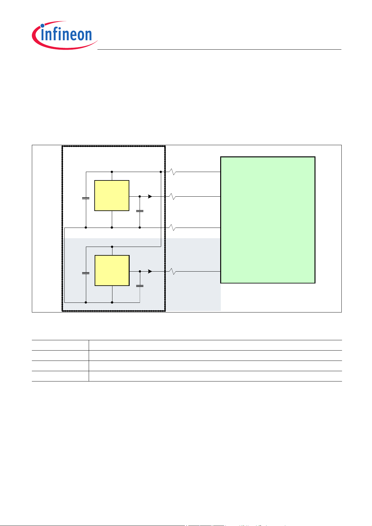
Figure 3-1 shows the connection of the TLE4997 to a programmer. The pins VDD and OUT of the sensor IC are
used for the digital programming interface as described in Table 3-1 (See datasheet of corresponding TLE4997
type for pinout).
Figure 3-1 Connection of TLE4997 to Programmer
Table 3-1 Pin Functions for Programming Interface
Pin Programming Function
VDD Programming interface clock
GND Ground
OUT Programming interface data I/O
User’s Manual 5 v01_01, 2019-08
Page 6
TLE4997
VDD
Vout
LSB MSB
duri ng first transmission , the output stage is stil l switch ed on
power up
interface
activated
internal buffer on
VDD
Vout
LSB MSB
during transmission the buffer is switched off internal buffer on
interface
active
interface
active
Z
protocol
output
leading driver
off pulse
protocol
output
User’s Manual
TLE4997 Programming
3.2 Programming Interface
3.2.1 Communication Scheme
The digital programming interface uses specific frames, which can have one of the two following functions:
• Command frames contain a specific task (e.g. read/write data, select EEPROM programming etc.) and a
corresponding address
• Data frames contain a 16 bit data value sent to or received from the device - these frames can only follow a
proper command frame for reading or writing data
A valid frame has the following properties:
• A frame consists of 21 bits in total
• A bit is shifted in or out via the output line with a rising clock edge on the supply line
• A frame always starts and ends with a '1' (frame bits)
• The LSB of a frame transmitted to the sensor is shifted in first
• The LSB of a frame replied by the sensor is shifted out first
• The whole frame sent to the device, including frame bits, is protected with an even positional and an odd
positional parity bit
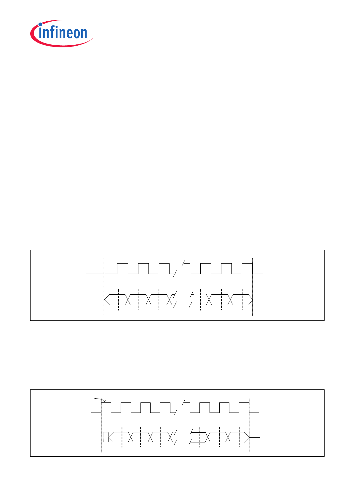
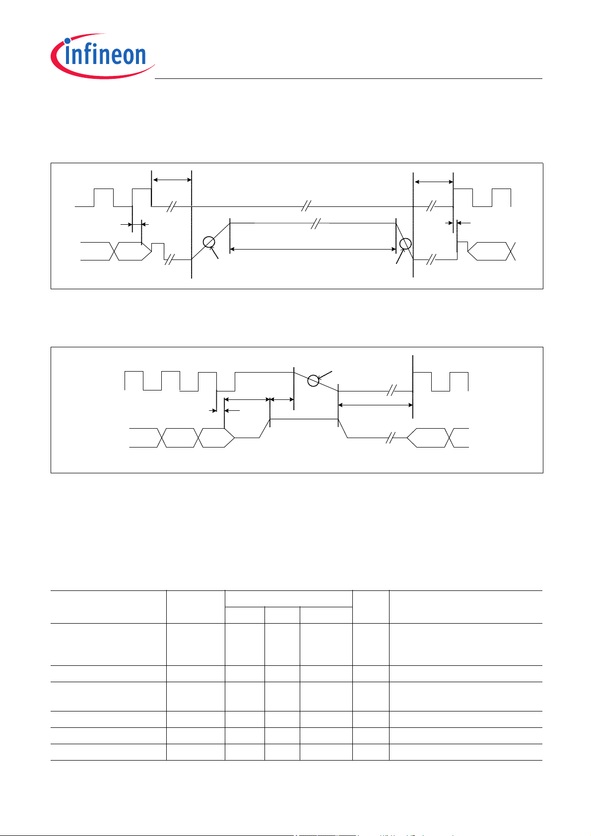
The first frame sent has to be a valid command to activate the interface mode and it has to be sent within 19ms
after power up. As an additional protection, the device does not deactivate its output stage during this transmission
(using 21 clock pulses) as shown in Figure 3-2. This means that the interface driver of the programmer needs to
overrule the open drain output stage of the sensor during this initial transmission.
Figure 3-2 First Frame Transmission to the Sensor
Attention: Overruling Vout requires a strong driver on the programmer, since the OUT line must be driven
to low levels close to GND for any “0”-bit and close to VDD for any “1”-bit in order to ensure a
proper communication with the sensor.
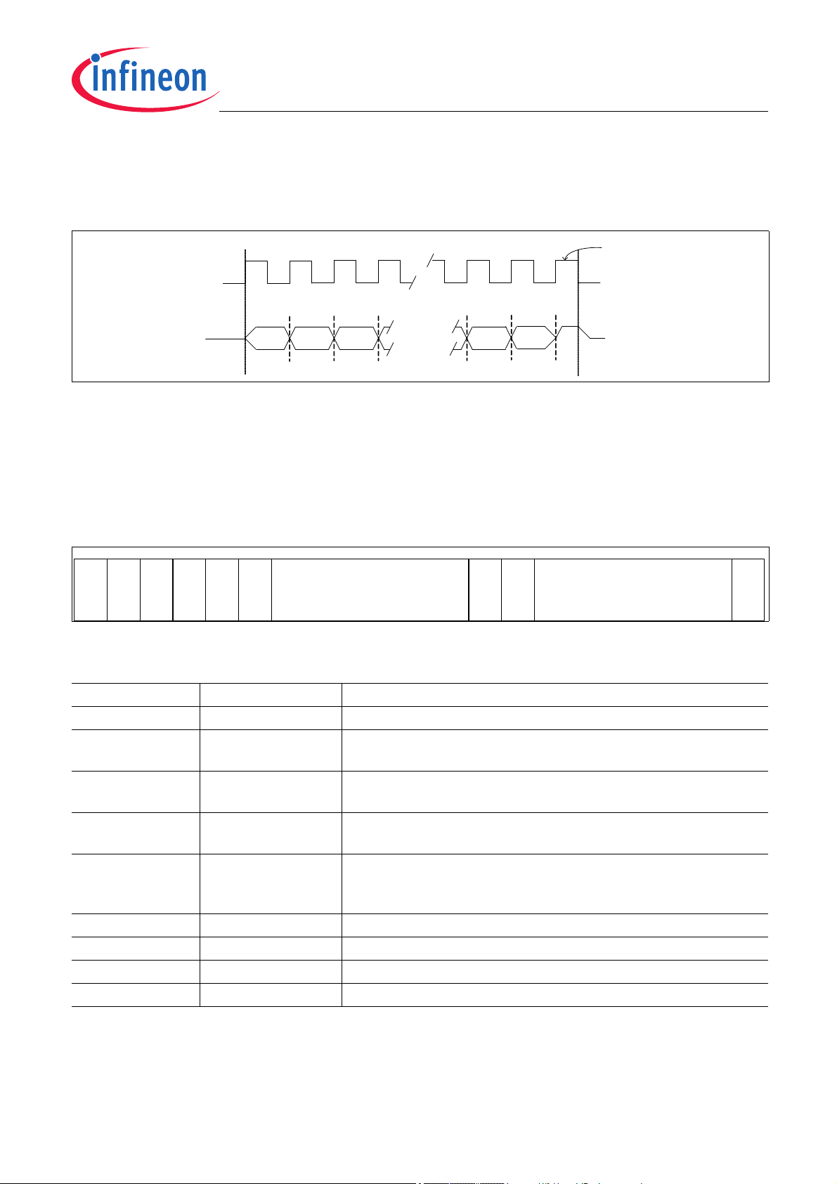
After the first frame, to avoid additional power consumption in the output stage of the device, the internal driver is
deactivated in programming mode while the sensor is receiving a frame. It is activated again after completion of
the transmission. This is illustrated in Figure 3-3.
Figure 3-3 Further Frame Transmisson from the Programmer to the Sensor (Write Access)
User’s Manual 6 v01_01, 2019-08
Page 7
TLE4997
VDD
Vout
LSB
MSB
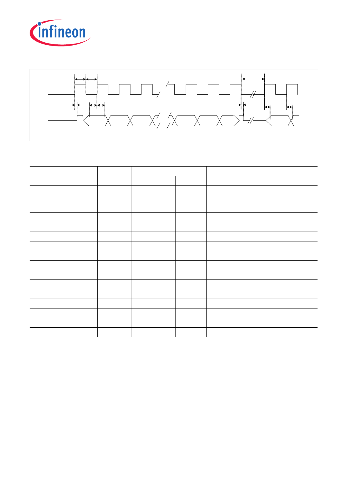
digital data readout, buffer in I/O mode
inte rnal buffer o n internal buffer on
tailing driver on
pulse
1 1
POP
E
0 0 ADDR (6bit) 1 0 CMD (6bit) 1
MSB (bit 20) LSB (bit 0)
User’s Manual
TLE4997 Programming
In case of a wrong command or data frame, the interface is immediately locked and the device falls back to its
normal application mode. The read access to the device is triggered by clock pulses on the supply line as shown
in Figure 3-4. The timing of read and write accesses is described in Chapter 3.3.2.
Figure 3-4 Frame Transmisson from the Sensor to the Programmer (Read Access)
3.3 Command Frame
The structure of a command frame is shown in Figure 3-5. Available commands are given in Table 3-2. The parity
bits PE (bit 17) and PO (bit 18) have to be set in the follwing way (bit 0 is the LSB, bit 20 is the MSB):
bit0 XOR bit2 XOR bit4 XOR …. XOR bit20 = 0
bit1 XOR bit3 XOR bit5 XOR …. XOR bit19 = 0
Figure 3-5 Command Frame Structure
Table 3-2 List of Available Commands
Command Bits (MSB...LSB) Function
0
H
1
H
000000 Leave programming mode
000001 Single data readout from given address without increment (sensor
1)
response: one data frame)
3
H
9
H
000011 Data readout from given address with increment (readout finishes
when address “xxx111
” is reached)
B
001001 Single data write to given address without increment (followed by
one data frame)
B
H
001011 Data write to given address with increment (followed by multiple data
frames; finishes at address “xxx111
B
command frame)
C
H
D
H
E
H
F
H
1) not to be followed by any data frame
2) followed by application of a programming pulse
3) followed by application of a margin voltage level before the last clock pulse falling edge
001100 Enable EEPROM write mode (programs “1”-bits)
001101 Enable EEPROM erase mode (programs “0”-bits)
001110 Enable EEPROM margin check mode (programs level check)
001111 EEPROM refresh (update EEPROM registers)
” or by sending another
1)2)
1)2)
1)3)
1)
User’s Manual 7 v01_01, 2019-08
Page 8

TLE4997
1 0
POP
E
DATA (16bit) 1
MSB (bit 20) LSB (bit 0)
1 ADR (3 LSBs) DATA (16bit) 1
MSB (bit 20) LSB (bit 0)
User’s Manual
TLE4997 Programming
3.3.1 Data Frame
The structure of a data frame sent to the device is shown in Figure 3-6. The parity bits PE (bit 17) and PO (bit 18)
have to be set in the same way as for the command frame (bit 0 is the LSB, bit 20 is the MSB):
bit0 XOR bit2 XOR bit4 XOR …. XOR bit20 = 0
bit1 XOR bit3 XOR bit5 XOR …. XOR bit19 = 0
Figure 3-6 Data Frame to Sensor
Figure 3-7 shows a the structure data frame received from the sensor. Instead of a zero bit followed by two parity
bits, the least significant 3 bits of the address used for the readout are transmitted together with the data. This is
to check the plausibility of the received data.
Figure 3-7 Data Frame from Sensor
3.3.2 Interface Specification
Table 3-3 specifies the operating conditions of the programming interface, which must be met in order to ensure
correct operation of the TLE4997 during programming. All specified parameters refer to these operating
conditions, unless otherwise noted.
Table 3-3 Operating Range of the Programming Interface
Parameter Symbol Values Unit Note / Test Condition
Min. Typ. Max.
Supply voltage V
Supply buffer capacitance C
Load capacitance C
Ambient temperature T
Number of programming
N
DD
S
L
PRG
PRG
cycles
Programming time
Programming start time
1) >47nF soldered to the device required in case that connectivity failures can influence the programming voltage.
t
PRG
t
PRG_START
4.5 – 5.5 V –
47 – 1000 nF VDD to GND
1)
0.0
– 210 nF OUT to GND
10 – 60 °C during programming
10 Cycles Programming is allowed only at
start of lifetime
– 100 – ms For complete memory
– – 19 ms To start programming mode, a
first read command shall be sent
within this time window after
power-up
The specification for timings and electrical levels of the programming interface is shown in Table 3-4. The meaning
of the timing parameters is illustrated in Figure 3-8.
User’s Manual 8 v01_01, 2019-08
Page 9
TLE4997
VDD
Vout
LSB MSB
t
cl
t
ch
tsut
hldt
del
t
hlm
LSB
t
set t
set
t
min
init
fram e
data read
frame
User’s Manual
TLE4997 Programming
Figure 3-8 Frame Timing
Table 3-4 Electrical and Timing Specification of the Programming Interface
Parameter Symbol Values Unit Note / Test Condition
Min. Typ. Max.
V
clock high level V
DD
DD,CLKHI
8.8 9.4 10 V specification of VDD operating
range does not apply to clock
V
clock low level V
DD
OUT data out high level V
OUT data out low level V
OUT data in high level V
OUT data in low level V
OUT data input current I
VDD clock high time t
V
clock low time t
DD
Data in setup time t
Data in hold time t
Data out settling time t
Time between frames t
Buffer off delay t
Buffer on delay t
DD,CLKLOW
O,OHIGH
O,OLOW
O,IHIGH
O,ILOW
O
CH
CL
SU
HLD
SET
MIN
DEL
HLM
1) capacity of external driver, especially during initial interface access (to overwrite ratiometric device output).
2) to reduce collisions with the ext. driver, it must be switched on slower than t
charge/discharge behaviour on V
OUT
3) to reach again a valid and stable ratiometric V
4.8 5 5.2 V
VDD - 2 – V
DD,CLKHI
V OUT follows V
0–2.0 V
3.0 V
DD
VDD + 0.1 V
-0.2 0.0 0.1 V
-50 – 50 mA
1)
2.4 50 100 µs 5k...250kBit/s
1.6 4.0 100 µs 5k...250kBit/s
1.5 2.0 – µs to rising V
2.3 3.0 – µs after rising V
– 1.0 1.7 µs after rising V
10.0 – – µs
10.0 25.0 – µs
– 5.0 10.0 µs
depends also on capacitive output load.
signal state, please check the power-on time in the data sheet.
OUT
DEL
2)
2)3)
min. and switched off faster than t
DD
DD
DD
DD
if ‘high’
HLM max.
;
User’s Manual 9 v01_01, 2019-08
Page 10
TLE4997
VDD
Vout
MSB
t
HLD
LSB
t
MIN
next command
frame
t
MIN
erase or write
command frame
(buffer stays off)
V
prog
puls e
V
O,PROG
/t
(rise)
V
O,PROG
/t
(fall)
t
PROG,WR
or t
PROG,ER
t
HLD
VDD
Vout
MSB LSB
t
MARG
next command
frame
t
min
margin
command frame
(buff er sta ys off)
Vdd/t
(fall)
t
hld
apply V
O,MARG
and
capture EEPROM data
t
min
User’s Manual
TLE4997 Programming
In order to permanently store a programmed parameter set to the EEPROM, the “EEPROM erase” and “EEPROM
write” commands shall be sent, followed by a programming pulse. Figure 3-9 shows the timing of the programming
pulse.
Figure 3-9 Programming Pulse Timing
After programming, a margin check is necessary to test the stability of the programmed data. The margin check
is initiated by an “EEPROM margin check” command followed by a margin voltage.
Figure 3-10 Margin Check Timing
The margin voltage is varied during subsequent steps within the threshold margin level range. A too low margin
voltage value indicates a too short programming pulse duration or a too low programming voltage. A too high
margin voltage value indicates a too long programming pulse duration or a too high programming voltage.
Table 3-5 gives the electrical and timing specifications of the programming pulse and the margin voltage check
procedure.
Table 3-5 Electrical and Timing Specification of the Programming Pulse and Margin Voltage
Parameter Symbol Values Unit Note / Test Condition
OUT data input current I
OUT margin level V
Threshold margin level V
Margin setup time t
V
DD
OUT program level V
User’s Manual 10 v01_01, 2019-08
Min. Typ. Max.
O
O,MARG
TH
MARG
slope for margin VDD/t 5 10 150 V/µs
O,PROG
0 – 20 mA during application of
-0.1 – 7 V
2.23 – 4.5
0.4
200 – – µs
19.2 19.3 19.4 V
V
V
programming pulse or margin
voltage
check “1”
check “0”
Page 11

TLE4997
User’s Manual
TLE4997 Programming
Table 3-5 Electrical and Timing Specification of the Programming Pulse and Margin Voltage (cont’d)
Parameter Symbol Values Unit Note / Test Condition
Min. Typ. Max.
OUT program slope
1)
(rise)
OUT program slope
1)
(fall)
OUT write time t
OUT erase time t
1) faster slope may lead to permanent damage of the EEPROM.
V
O,PROG
V
O,PROG
PROG,WR
PROG,ER
/t – – 2 V/µs time to reach V
O,PROG
shall not
exceed 50 µs
/t -10 – – V/µs time to reach 1v max. shall not
exceed 50 µs
9.9 10.0 10.1 ms
79.2 80.0 80.8 ms
3.4 Register Map
Table 3-6 shows the internal registers of the TLE4997 (compare also Figure 2-1).
Table 3-6 TLE4997 Register Map
Address Symbol Function R/W
05
06
07
0A
0B
0F
10
20
21
H
H
H
H
H
H
...19
H
H
H
H
HCAL Calibrated Hall value read only
TCAL Calibrated temperature value, including reference temperature T0read only
VDAC Calculated DAC value, incl. clampling read only
HADC Uncalibrated Hall ADC value read only
TADC Uncalibrated temperature ADC value read only
STATUS Status register read only
EEPROM EEPROM registers (see Chapter 3.5) read/write
DAC_SET Direct setup of DAC value read/write
TEST Test mode register read/write
Note: To access the registers (except STATUS, HADC, TADC, VADC, DAC_SET and TEST), the digital signal
processing unit (DSPU) has to be disabled first via the TEST register.
HCAL
This register contains the temperature compensated magnetic measurement as a 16bit signed value. This value
is in the range of +/- 30000.
TCAL
This register contains a 16 bit signed value and delivers the current junction temperature of the device. The
junction temperature in °C is calculated from the register value by: T
= (TCAL/16+48) [°C].
J
VDAC
This register contains a 12 bit unsigned decimal result applied to the internal DAC for the ratiometric output stage.
The value range is from 0 to 4095 and corresponds to 0% to 100% of V
DD
.
HADC
This register contains a 16bit signed value that corresponds to the raw Hall cell measurement value. This value is
in the range of +/- 20000.
User’s Manual 11 v01_01, 2019-08
Page 12

TLE4997
15 14 13 12 11 10 9 8 7 6 5 4 3 2 1 0
LSB
ROMSIG4
perr_more
LOCKED
perr_adr0
CRC ok
perr_adr1
perr_adr2
perr_adr3
HWver0
ROMSIG3
ROMSIG2
ROMSIG1
ROMSIG0
HWver1
HWver2
perr_col
15 14 13 12 11 10 9 8 7 6 5 4 3 2 1 0
LSB
FEC off
DAC test
DSP stop
REF off
DSP off
0
0
0
0
0
0
0
0
0
0
0
MSB
User’s Manual
TLE4997 Programming
TADC
This register contains a 15bit unsigned raw temperature value.
STATUS
The content of the status register is shown in Figure 3-11.
Figure 3-11 Status Register
• CRC ok has to be “1”, otherwise the DSP built-in self-test was failed and the device is defective
• LOCKED must be ’0’ as long as the lockbits are not programmed. After setting the lockbits the lock can be
verified by refreshing the EEPROM content and checking this bit before the supply of the device is removed
or the interface is closed.
• perr_adr has to be on address F
(“1111B”), otherwise it shows the first EEPROM address where the internal
H
parity check failed.
• perr_more must be “0”, otherwise more than one EEPROM address has a parity error.
• perr_col must be “0”, otherwise one or more EEPROM columns have a parity error.
• HWver contains the actual silicon revision starting with 0 (=”000”). The latest version from 8’ manufacturing line
is version 3 (=”011”, availability from mid 2006 and released for productive use).
• ROMSIG has to be 1F
, otherwise the DSP ROM is not valid and the device is defective.
H
DAC_SET
This register contains a 12 bit unsigned decimal value. When the DAC test bit is set, the value of this register is
used on the ratiometric output.
TEST
The content of the test register is shown in Figure 3-12. All bits are “0” after reset. All bits not described or used
shall be kept at “0”.
Figure 3-12 Test Register
• “Margin zero on” is used to select the margin test mode. It is set to ‘1’ for testing the EEPROM threshold
voltages of cells programmed to ‘0’, and it is set to ‘0’ for testing the EEPROM threshold voltages of cells
programmed to ‘1’.
• “FEC off” switches off the error correction of the EEPROM. This bit has to be set when reading the EEPROM
content.
• “REF off” switches off the automatic (cyclic) refresh performed by the DSP to actualize the EEPROM registers
from the EEPROM cells. This bit has to be set when writing new values to the EEPROM registers.
User’s Manual 12 v01_01, 2019-08
Page 13

TLE4997
ADDR Description 15141312111009080706050403020100
10
H
Parity of each column PlPcPcPcPcPcPcPcPcPcPcPcPcPcPcP
c
11
H
IC lock high, USER,
clamping low
P
l
LH USER CL - Clamping low (bit 11...0)
12
H
Clamping high value PlReserved CH - Clamping high (bit 11...0)
13
H
Gain P
l
G - Gain (bit 14...0)
14
H
Offset P
l
OS - Offset (bit 14...0)
15
H
TQ value, TT value P
l
TQ - quadratic temperature
coefficient (bit 7...0)
precal area - do not modify
TT - register (bit 6 … 0)
16
H
LP value, Range, TL
Value, IC lock low
P
l
LP -
(bit 0,2,1)
R-
(bit 1,0)
TL - linear temperature coefficient (bit
8…0)
LL
17
H
Reserved P
l
Reserved - do not modify
18
H
Reserved P
l
Reserved - do not modify
19
H
Reserved P
l
Reserved - do not modify
User’s Manual
• “DSP off” switches off the signal processing unit (DSP). This bit has to be set prior to accessing the internal
register values via the interface (HCAL, TCAL, SCAL and EEPROM).
• “DSP stop” has to be set prior to switching the DSP off (as a separate command) before reading out the
calculated data HCAL, TCAL, and/or SCAL. This allows the DSP to finish the calculation of the current sample
and all values in the RAM are consistent.
• “DAC test” switches from the DSP DAC value to the DAC_SET value. This allows setting any DAC value
directly to measure the output voltage for a given DAC value for calibration proposes.
TLE4997 Programming
3.5 EEPROM Map
Figure 3-13 shows the content of the EEPROM registers.
low pass
Range
Figure 3-13 EEPROM Map of TLE4997 (all types).
The fields marked in red are configuration parameters for the sensor hardware. Those marked in yellow are used
by the DSP algorithms for signal processing. The purple fields are used to determine the condition of the
parameters by an external programming software (user defined) and the blue and cyan fields are parity bits for the
corresponding lines and columns used by the internal forward error correction (FEC). All parameters are unsigned
integer values. The reserved fields marked in white shall not be changed.
The functional description of the configuration and calibration parameters in the EEPROM map is given in
Chapter 4.
Parity Bits
The parity P
bit4, ... bit14) and the parity P
line (address 0x10 ... 0x19) needs to be calculated so that the sum of its bits is always odd.
Note: Before accessing the EEPROM, the forward error correction (FEC) shall be disabled via the TEST register.
User’s Manual 13 v01_01, 2019-08
of each column (including the precalibration ranges) is even for even bit positions (bit0=LSB, bit2,
c
for all odd columns (bit1, bit3, ... bit15=MSB) is odd. The parity Pl of every EEPROM
I
Page 14

TLE4997
User’s Manual
TLE4997 Programming
User Bits
The two USER bits are free bits which can be used by the system integrator, for example to track calibration steps.
Lock Bits
LH and LL are lock bits (LH locked if '1', LL locked if '0'). If either LH, LL or both are set to locked state, the
programming interface cannot be accessed anymore.
3.6 Programming Flow
The programming flow diagram in Figure 3-14 shows the procedural steps to setup the EEPROM content and to
program new values (EEP_NEW). EEP_PROG means the intermediate values stored in the EEPROM register
and EEP_OLD means the initial (old) EEPROM content.
Flowchart description:
1. Switch on the device.
2. Send an initial command (status register readout):
Check that the status is valid (Status register = F93D
and check the failure.
3. Set the register bits FECoff = 1, DSPoff = 1, REFoff = 1 (allows EEPROM access).
4. Read out the EEPROM content to an array EEP_OLD (store also for reference purpose and traceability)
In parallel: Prepare the data that shall be programmed as an array EEP_NEW.
5. Calculate the bits to be cleared from EEP_OLD to EEP_NEW as EEP_PROG array.
6. Write the EEPROM content from the EEP_PROG array to the EEPROM registers
7. Send the EEPROM erase command
Apply an erase programming pulse on the output pin (see Chapter 3.3.2).
8. Calculate the bits to be set from EEP_OLD to EEP_NEW as EEP_PROG array.
9. Write the EEPROM content from the EEP_PROG array to the EEPROM registers.
10. Send the EEPROM write command
Apply a write programming pulse on the output pin (see Chapter 3.3.2).
11. Send the EEPROM margin command
During the falling edge of the margin pulse on V
12. Read out the EEPROM content to the array EEP_PROG.
13. Verify the EEP_PROG data against EEP_NEW to check the programming (no bits flipped)
Optionally, steps 11 to 13 can be looped to find the exact margin threshold voltage.
If the margin threshold voltage is too low, do not continue and check the failure.
14. Check the status register again.
or F B3DH, compare Chapter 3.4), if not, do not continue
H
, apply V
DD
on the output (see Chapter 3.3.2).
O,MARG
User’s Manual 14 v01_01, 2019-08
Page 15

TLE4997
EEP_OLD
EEP_NEW
EEP_PROG
EEP_OLD
EEP_NEW
EEP_PROG
For each line I from 0x10 to 0x19:
EEP_PROG[i] = (EEP_OLD[i] XOR EEP_NEW[i]) AND EEP_NEW[i]
(as precal areas must not be changed, the bits in this areas must remain ‚0')
Readout could be looped f or s everal
margin v oltages (s tarting from a very
high volt age e. g. 5V) to find the margin
level of t he EEPR OM
see abov e (lik e c omplete
readout proc edure f or
EEP_OLD)
EEPROM
programming
INIT-CMD:
cmd=0x 01
adr=0x0F
READ DAT A
Vdd = 5V
Is
0xF93D or
0xF B3D ?
ILLEGAL
STATU S:
analyse
problem
NO
CMD (write):
cmd=0x 09
adr=0x21
DAT : 0x0640
(DSP, FEC ,
REF off)
CMD (b read)
cmd=0x 03
adc=0x 10
RD. B-DATA
CMD (read)
cmd=0x 01
adc=0x 18
READ DATA
CMD (read)
cmd=0x 01
adc=0x 19
READ DATA
10x 16bit
> EEP_OLD <
Store this initial
dataset (allow s
later res tore)
> EEP_NEW <
Given by TC
setup and/or 2P
algorithms etc.
User input, T C
setup algorithm or
2P calibrat ion
algorithm set up
Create erase
pattern for
programming
2x 10x 16bit
CMD (bwrite)
cmd=0x 0b
adc=0x 10
WR. B-DATA
CMD (write)
cmd=0x 09
adc=0x 18
WR. DATA
CMD (write)
cmd=0x 09
adc=0x 19
WR. DATA
CMD (eras e):
cmd=0x 0D
adr=0x00
V
prog
PULSE
Create wri te
pattern for
programming
2x 10x 16bit
CMD (write):
cmd=0x 0C
adr=0x00
V
prog
PULSE
CMD(marg.):
cmd=0x 0E
adr=0x00
V
mar g+Vdd
-ra mp
CMDs (read)
cmd=0x 03/01
adr=0x10/8/ 9
READ DATA
content =
EEP_NEW ?
ILLEGAL
MARGIN
READ:
analyse
problem
NO
FIN ISH ED
margin higher
required limit ?
NO
Vdd = 0V (off)
For each line I from 0x10 to 0x19:
EEP_PROG[i] = INVERT ((EEP_OLD[i] XOR EEP_NEW[i]) AND EEP_OLD[i])
(as precal areas must not be changed, the bits in this areas must remain ‚1')
Optionally do a last status
readout (adr. 0x 0F) to c heck
the I F mode is still act ive
and the devic e is ok.
User’s Manual
Figure 3-14 Programming Flow
The following chapters give a more detailed description of individual steps of the programming flow:
User’s Manual 15 v01_01, 2019-08
TLE4997 Programming
Page 16

TLE4997
User’s Manual
3.6.1 Setting the TEST register
The following steps are used to set the TEST register:
1. Send a write command (TEST register set: Command 09
, Adress: 21H).
H
2. Send a new data word for the register.
3.6.2 Readout of the EEPROM Content
The following steps are used to readout the EEPROM and store the content in an array:
1. Send a block read command (EEPROM data readout: Command 03
, Address: 10H).
H
2. Read the first 8 data words of the EEPROM and store it in an array.
3. Send a read command (EEPROM data readout: Command 01
, Address: 18H).
H
4. Read the 9th data word of the EEPROM and store it in an array.
5. Send a read command (EEPROM data readout: Command 01
, Address: 19H).
H
6. Read the 10th data word of the EEPROM and store it in an array.
3.6.3 Setting the EEPROM Content
The following steps are used to set the EEPROM content with data from an array:
1. Send a block write command (EEPROM data write: Command 0B
2. Send the first 8 data words from the array to the EEPROM.
3. Send a write command (EEPROM data write: Command 09
H
4. Send the 9th data word from the array to the EEPROM.
5. Send a write command (EEPROM data write: Command 09
H
6. Send the 10th data word from the array to the EEPROM
, Address: 10H).
H
, Address: 18H).
, Address: 19H).
TLE4997 Programming
3.6.4 Calculation of Bits to Erase
The EEP_PROG array for the erase procedure is calculated from the old EEPROM content EEP_OLD and the
new EEPROM content EEP_NEW in the following way:
For each data word i: EEP_PROG[i] = INVERT ((EEP_OLD[i] XOR EEP_NEW[i]) AND EEP_OLD[i])
Table 3-7 shows an example of a calculated erase mask.
Table 3-7 Erase Array Example
EEP_OLD 0101010101010101
EEP_NEW 0101110001010101
EEP_PROG 1111111011111111
3.6.5 Calculation of Bits to Write
The EE P_PROG array for the wr ite procedure is calculated from the old EEPROM content EEP_OLD and the new
EEPROM content EEP_NEW in the following way:
For each data word i: EEP_PROG[i] = (EEP_OLD[i] XOR EEP_NEW[i]) AND EEP_NEW[i]
Table 3-7 shows an example of a calculated erase mask.
Table 3-8 Write Array Example
EEP_OLD 0101010101010101
EEP_NEW 0101110001010101
EEP_PROG 0000100000000000
User’s Manual 16 v01_01, 2019-08
Page 17

TLE4997
EEPROM
programm ing
INIT-CMD:
cm d=0x01
adr=0x0F
READ DAT A
Vdd = 5V
Is
0xF 93D or
0xFB3D ?
ILLEGAL
STATUS:
analys e
problem
NO
CMD (write):
cm d=0x09
adr=0x21
DAT: 0x0800
(DSP stop)
FINISHED
Vdd = 0V (off)
Optionally do a last status
readout (adr. 0x0F) to check
the IF mode is still active
and t he dev ice is ok .
CMD (read)
cm d=0x01
adr=0x05
READ DATA
CMD (wr ite):
cm d=0x09
adr=0x21
DA T: 0x0C00
(DSP stop,
DSP off)
Like reading out H_CAL,
also all other RAM and
EEPROM registers c an
be read out here in a loop.
User’s Manual
TLE4997 Programming
3.6.6 Margin Voltage Check
The threshold voltage of EEPROM cells is dependent on the programming voltage and programming pulse length.
For reliable programming the programming pulse has to be kept within the specification (Table 3-5) at the sensor
interface. The margin command can be used to check the threshold voltages of the programmed cells:
To check the cells programmed to '1', a voltage V
E
). For EEPROM cells with a threshold voltage smaller than the applied V
H
EEPROM registers, for those with a higher threshold voltage, a '1' will be written. By sweeping the applied V
is applied after the margin check command (Command
O,MARG
, a '0' will be stored to the
O,MARG
O,MARG
the actual threshold voltages of each EEPROM cell can be identified.
In order to check the threshold voltages of EEPROM cells programmed to ‘0’, it is necessary to activate the “Margin
zero on” bit in the TEST register before sending the margin check command. Also for the ‘0’ cells, the actual
threshold voltages of each EEPROM cell can be identified, by sweeping the applied V
O,MARG
.
3.6.7 DATA access example
Following steps are required to readout other internal data like the calibrated temperature and Hall value (as
shown below in Table 3-15). This routines can also be used for an EEPROM access (in that case also FECoff
should be set to ’1’).
,
Figure 3-15 Basic data access flow
Flowchart description:
1.
Switch on the device
2. Send an inital command (status register readout)
3. Read the status data,check that the device is valid and the EEPROM content is valid
4. Set the test register: DSP stop=1 (see previous chapter)
5. Set the test register: DSP stop=1 DSP off=1 (see previous chapter)
6. Send a read command (HCAL)
– Read the data word
User’s Manual 17 v01_01, 2019-08
Page 18

TLE4997
EEPROM
programm ing
INIT-CMD:
cm d=0x01
adr=0x0F
READ DATA
Vdd = 5V
Is
0xF93D or
0xFB3D ?
ILLEGAL
STATUS:
analyse
problem
NO
CMD (write):
cm d=0x09
adr=0x21
DAT: 0x0640
(DSP, F EC,
REF off)
FINISHED
Vdd = 0V (off)
Optionally do a las t st atus
readout (adr. 0x0F ) t o c heck
the IF m ode is s till act ive
and the device is ok.
All ot her EEPR OM
regis ters can be
written here in a loop
(as re qui red ).
CMD (wri te)
cm d=0x09
adr=0x10.. 19
WR. DATA
CMD (write):
cm d=0x09
adr=0x21
DAT: 0x0250
(FEC, R EF
off)
Here the output should
show (temporarily) the
desired result (before
switc hing off the
supply, of co urse).
User’s Manual
TLE4997 Programming
– This readout might be looped for reading out also other parameters (like TCAL)
7. Check the status register again
Note: This routine can be merged with other (exemplary shown) routines. In that case only one initial frame (the
very first interface access) is required after power-on.
3.6.8 Temporary overwrite of EEPROM data
Following steps are required to readout other internal data like the calibrated temperature and Hall value (as
shown below Table 3-16). As the error correction stays disabled, it is not necessary to use correct parity values
for this temporary setup. In case the parity is always corrected (and it is desired to check the complete behavior
and correct EEPROM array calculation), the “FECoff” bit could be switched off again after the temporary EEPROM
write.
Figure 3-16 Basic EEPROM register overwrite flow
Flowchart description:
1. Switch on the device
2. Send an inital command (status register readout)
3. Read the status data,check that the device is valid and the EEPROM content is valid
4. Set the test register: DSP off=1 FEC off=1 REF off=1 (see previous chapter)
5.
Send a write command (for any EEPROM register)
Send the data words (in 16bit format, MSBs containing the parity may be kept ’0’)
6. Set the test register: FEC off=1 REF off=1 (see previous chapter)
- The device is now temporarily working with the new EEPROM setting.
7. Check the status register again
User’s Manual 18 v01_01, 2019-08
Page 19

TLE4997
EEPROM
programm ing
INIT-CMD:
cm d=0x01
adr=0x0F
READ DATA
Vdd = 5V
Is
0xF93D or
0xFB3D ?
ILLEGAL
STATUS:
analyse
problem
NO
CMD (write):
cm d=0x09
adr=0x21
DAT: 0x4000
(DAC test)
FINISHED
Vdd = 0V (off)
Optionally do a las t st atus
readout (adr. 0x0F ) t o c heck
the IF m ode is s till act ive
and the device is ok.
Set all required DAC
values in a loop
CMD (wri te)
cm d=0x09
adr=0x20
WR. DATA
Wait 10ms and
evaluate the
response on
the V
out
-pin
User’s Manual
TLE4997 Programming
3.6.9 DAC setup example
To find the exact DAC value for a desired output voltage (e.g. to set up the clamping low/high registers with the
best available accuracy), it is possible to set the DAC value directly and to measure the result on the output pin.
Figure 3-17 Basic DAC setup flow
Flowchart description:
1. Switch on the device
2. Send an inital command (status data readout)
Read the status data,check that the device is valid and the EEPROM content is valid
3.
4. Set the test register: “DAC Test”=1 (see previous chapter)
- The output immediately shows the content given by the DAC_SET register.
5. Send a write command (DAC_SET register)
- Send the data word for the desired 12bit DAC value (in 16bit format, MSBs are ’0’)
- The output changes accordingly to the new DAC value in DAC_SET
6. After 10ms (max. output setup time), measure Vout
- Repeat writing a new DAC value (continue at step 5) until the response of all desired DAC values are measured
7. Check the status register again
User’s Manual 19 v01_01, 2019-08
Page 20

TLE4997
Gain
G 16384–()
4096
------------------------------
=
V
OS
OS 16384–()
4096
---------------------------------
V×
DD
=
User’s Manual
Configuration & Calibration Parameters
4 Configuration & Calibration Parameters
This chapter describes the configuration and calibration parameters that can be set in the EEPROM of the
TLE4997 (see EEPROM map, Chapter 3.5)
4.1 Magnetic Field Range - R
Table 4-1 Range Setting
Parameter R Range Nominal Range in mT
3Low ±50
2)
1
0 High ±200
1) Absolute accuracy of range values is not specified.
2) Setting R = 2 is not used, internally changed to R = 1.
Mid ±100
4.2 Gain Setting - G
The overall sensitivity is defined by the range and the gain setting. The output of the ADC is multiplied by the Gain
value. The Gain value is given by:
1)
(4.1)
Table 4-2 Gain
Parameter Symbol Values Unit Note / Test Condition
Min. Typ. Max.
Gain range Gain - 4.0 – 3.9998 –
Gain quantization steps ΔGain – 244.14 – ppm Corresponds to 1/4096
1) For Gain values between -0.5 and +0.5, the numerical accuracy decreases.
To obtain a flatter output curve, it is recommended to select a higher range setting.
2) In 100 mT range, a gain value of +1.0 corresponds to typically 40mV/mT. Infineon pre-calibrates the samples to 60mV/mT..
It is recommended to do a final 2-point calibration of each IC within the application.
1)2)
4.3 Offset Setting - OS
The offset value corresponds to an output voltage with zero field at the sensor. The offset value can be calculated
by:
(4.2)
User’s Manual 20 v01_01, 2019-08
Page 21

TLE4997
User’s Manual
Configuration & Calibration Parameters
Table 4-3 Offset
Parameter Symbol Values Unit Note / Test Condition
Min. Typ. Max.
Offset range
Offset quantization steps ΔOUT
1) Infineon pre-calibrates the samples at zero field to typically 50% output value in 100 mT range. It is recommended to do a
final 2-point calibration of each IC within the application.
1)
V
OS
-400 – 399 %V
– 1.22 – mV at VDD = 5V
OS
DD
generally V
DD
/4095
4.4 Low-Pass Filter - LP
A configurable digital low-pass filter is implemented at the output of the Hall ADC. The possible settings are shown
in Table 4-4. Figure 4-1 shows the filter characteristics as a magnitude plot for the settings 78 Hz to 1320 Hz (from
left to right). The update rate of the low-pass filter output is nominally 16 kHz.
Attention: The bit arrangement of the LP-Filter register is "0,2,1" (see EEPROM map in Figure 3-13).
Therefore, the bits have to be rearranged accordingly to obtain the desired configuration. For
example, the LP-filter setting "6" corresponds to the binary "011" in the LP-filter register.
Table 4-4 Low Pass Filter Setting
Parameter LP Nominal cutoff frequency in Hz (-3 dB point)
078
1244
2421
3615
4826
5 1060
6 1320
7Off
User’s Manual 21 v01_01, 2019-08
Page 22

TLE4997
10
1
10
2
10
3
0
-6
-5
-4
-3
-2
-1
Magnitude (dB)
Frequency (Hz)
10
1
10
2
10
3
0
-6
-5
-4
-3
-2
-1
Magnitude (dB)
Frequency (Hz)
10
4
User’s Manual
Figure 4-1 DSP Input Filter (Magnitude Plot)
Configuration & Calibration Parameters
Table 4-5 Low-Pass Filter
Parameter Symbol Values Unit Note / Test Condition
Min. Typ. Max.
Corner frequency variation Δ
f -25 – +25 % –
4.5 DAC Input Interpolation Filter
An interpolation filter is placed between the DSP and the output DAC. This filter determines the frequency behavior
of theTLE4997 in case the DSP input filter is disabled input filter is disabled . The update rate after interpolation
filter is 256 kHz
Figure 4-2 DAC Input Filter (Magnitude Plot)
User’s Manual 22 v01_01, 2019-08
Page 23

TLE4997
0
1
B
min
B (mT)
B
max
V
out
(V)
5
2
4
3
Error range
Error range
Operating range
V
CLH
V
CLL
V
CLL
CL
4096
------------
VDD×=
User’s Manual
Configuration & Calibration Parameters
4.6 Clamping - CH, CL
The clamping function is useful for separating the output range into an operating range and error ranges. If the
magnetic field is exceeding the selected measurement range, the output voltage V
values. Any value in the error range is interpreted as an error by the sensor counterpart.
Figure 4-3 shows an example in which the magnetic field range between B
and B
min
between 0.8 V and 4.2 V.
is limited to the clamping
OUT
is mapped to voltages
max
Figure 4-3 Clamping Example
Clamping - TLE4997 :
Table 4-6 Clamping
Parameter Symbol Values Unit Note / Test Condition
Min. Typ. Max.
DD
1)
1)
) < V
V
CLL
V
CLH
CLQ
CL
) < V
DD
< ( 94% of VDD) for 120°C < TJ ≤ 150°C
OUT
<(95% of VDD) for T
OUT
0 – 99.98 %V
0 – 99.98 %V
–1.22–%mVat V
-15 15 mV in lifetime
≤ 120°C
J
DD
DD
= 5 V
DD
2)
over temperature
2)
Clamping low
Clamping high
Clamping quantization steps ΔV
Clamping voltage drift ΔV
1) If clamping is set it must be within the allowed output range.
2)Valid in the range (5% of V
and (6% of V
The clamping values are calculated by:
Clamping low voltage :
(4.3)
User’s Manual 23 v01_01, 2019-08
Page 24

TLE4997
V
CLH
CH
4096
------------
VDD×=
User’s Manual
Configuration & Calibration Parameters
Clamping high voltage:
(4.4)
4.7 Temperature Compensation - TL, TQ & TT
The TLE4997 has an integrated third-order temperature compensation using the coefficients TL, TQ, and TT,
which is used to compensate the thermal drift of the Hall cell (pre-configured by Infineon).
The magnetic field strength of a magnet depends on the temperature. This material constant is specific for the
different magnet types. The temperature compensation parameters TL and TQ of the TLE4997 can be adapted to
compensate this temperature dependency of the magnet in the application. The TT value is fixed and cannot be
modified.
Three parameters are used for the application temperature compensation:
• Reference temperature T
• A linear part (1st order) TC
• A quadratic part (2nd order) TC
The detailed procedure to derive the optimum TL and TQ parameters for a a given magnet characteristic is
described in Chapter 5.
0
1
2
Table 4-7 Temperature Compensation
Parameter Symbol Values Unit Note / Test Condition
Min. Typ. Max.
st
1
order coefficient TC
1
Quantization steps of TC
nd
2
order coefficient TC
2
Quantization steps of TC
Reference temp. T
1) Relative range to Infineon TC1 temperature pre-calibration, the maximum adjustable range is limited by the register-size
and depends on specific pre-calibrated TL setting, full adjustable range: -2441 to +5355 ppm/°C.
2) Relative range to Infineon TC2 temperature pre-calibration, the maximum adjustable range is limited by the register-size
and depends on specific pre-calibrated TQ setting, full adjustable range: -15 to +15 ppm/°C2.
TC
1
ΔTC
1
2
TC
ΔTC
0
1
2
2
-1000 – 3000 ppm/ °C
– 15.26 – ppm/ °C –
-6 – 6 ppm/ °C²
– 0.119 – ppm/ °C² –
-48 – 64 °C –
1)
2)
User’s Manual 24 v01_01, 2019-08
Page 25

TLE4997
S
DSP
TCAL()1
TL 160–
8 8192⋅
----------------------
TCAL
16
----------------
⎝⎠
⎛⎞
TQ 128–
1024 8192⋅
----------------------------
TCAL
16
----------------
⎝⎠
⎛⎞
2
TT 64–
131072 8192⋅
----------------------------------
TCAL
16
----------------
⎝⎠
⎛⎞
3
⋅+⋅+⋅+=
TCAL 16 TJ48–()⋅=
S
AppTJ
() 1TC1TJT0–()TC2TJT0–()
2
++=
User’s Manual
Calibration of TLE4997 Temperature Compensation
5 Calibration of TLE4997 Temperature Compensation
A temperature compensation mechanism is implemented in the TLE4997 to account for thermal drift of the Hall
probe sensitivity and thermal reduction of the remanent magnetization of a permanent magnet used in a position
sensing application. Initially, the TLE4997 is pre-configured by Infineon to have a constant magnetic sensitivity
over temperature.
In case the TLE4997 is used to measure an absolute magnetic field, for example in a current sensing application,
then no additional adaption of the temperature compensation by the user is required.
If the TLE4997 is used in a position sensing application where it measures the magnetic field generated by a
moving permanent magnet, then it is typically desired that the output signal of the TLE4997 depend only on the
magnet position. In this case, a user adaptation of the temperature compensation is required to account for thermal
reduction of the magnet’s remanence. Therefore, the TLE4997 has to be configured to increase its sensitivity
accordingly with increasing temperature to compensate the thermal reduction of the remanence.
This temperature coefficient of the remanence depends on the chosen magnet material, so the temperature
compensation of the TLE4997 has to be adapted to the permanent magnet employed in the application.
5.1 Integrated Temperature Polynomial
The integrated temperature compensation of the TLE4997 uses a third order polynomial, as shown in
Equation (5.1).
(5.1)
with:
(5.2)
T
is the junction temperature in °C. The coefficients TL, TQ, and TT are the linear, quadratic and cubic
J
temperature compensation coefficients, respectively. They are stored in the EEPROM and pre-configured by
Infineon for a constant magnetic sensitivity over temperature (see Chapter 3.5 for EEPROM map).
The coefficients TL and TQ can be adapted by the user to implement a compensation of the thermal reduction of
a magnet’s remanence. The coefficient TT is fixed to the value pre-calibrated by Infineon. It cannot be adapted.
5.2 Application Sensitivity Polynomial
In order to find the optimum TL and TQ parameters to minimized the position signal error due to the thermal
reduction of the magnet’s remanence, an application sensitivity polynomial has to be derived from a sensitivity
measurement in the application over temperature that describes the desired sensitivity factor as a function of
temperature (see Chapter 5.3). The application sensitivity polynomial is given by Equation (5.3).
(5.3)
T
is the junction temperature in °C, TC1 (in ppm/°C) and TC2 (in ppm/°C2) are the first and second order
J
application temperature coefficients and T
(in °C) is a reference temperature.
0
User’s Manual 25 v01_01, 2019-08
Page 26

TLE4997
0,925
0,950
0,975
1,000
1,025
1,050
1,075
-50 0 50 100 150
Rel. Change
TJ(°C)
MR(T)
Sapp(T)
MR(T)*Sapp(T)
S
AppTJ
()MRTA()cons ttan≈⋅
T
J
T
A
R
th
UI⋅()⋅+=
S
DSPfinalTJ
()S
DSPpreTJ
()S
AppTJ
()⋅≈
User’s Manual
Calibration of TLE4997 Temperature Compensation
Figure 5-1 Example thermal behavior of magnetic remanence M(T) and application sensitivity polynomial
S
(T) with reference temperature 48°C.
app
The reference temperature T
is a degree of freedom that can be chosen by the user, such that the gain of the
0
TLE4997 that is configured in the EEPROM, applies at this reference temperature.
In case the calibration of the offset and gain for the output charateristic is done after the calibration of the
temperature compensation, the choice of T
configured separately. A choice of T
= 48°C is recommended for simplicity (to match the reference temperature
0
is not relevant. In this case, the gain at a specific temperature is
0
in the definition of TCAL in Equation (5.2)).
The application sensitivity polynomial S
has to be determined in the application to approximately cancel the
App
temperature dependency of the remanence, as stated in Equation (5.4) and illustrated in Figure 5-1.
(5.4)
is the remanence of the permanent magnet as a function of temperature and TA is the ambient temperature in
M
R
the application that relates to the junction temperature T
by Equation (5.5).
J
(5.5)
is the thermal resistance of the TLE4997 as specified in the data sheet, U is the supply voltage and I is the
R
th
supply current.
After determining the application sensitivity polynomial S
sensor parameters TL
and TQ
final
for the final sensor configuration have to be adapted to combine the
final
compensation of the Hall sensing element drift (given by the precalibrated values TL
cancellation of the thermal reduction of the magnet’s remanence (given by S
from a sensitivity measurement over temperature, the
App
and TQ
pre
), as stated in Equation (5.6).
App
) and the
pre
(5.6)
S
DSPfinal(TJ
Equation (5.2), with the final parameters TL
with the pre-configured parameters TL
) is the integrated temperature polynomial given by the combination of Equation (5.1) and
and TQ
final
and TQ
pre
pre
.
After determination of the application sensitivity polynomial coefficients and readout of the pre-configured TL
TQ
, and TT parameters via the programming interface, the optimum TL
pre
. S
final
DSPpre(TJ
) is the integrated temperature polynomial
final
and TQ
parameters have to be
final
derived from Equation (5.6) and programmed into the TLE4997.
pre
,
User’s Manual 26 v01_01, 2019-08
Page 27

TLE4997
B(T)
Movement
N S
TLE4997
S
i()
VDAC
0
VDAC
i()
VDAC
0
–
-------------------------------------------------
=
User’s Manual
Calibration of TLE4997 Temperature Compensation
5.3 Determination of Sensitivity Polynomial from Measurement
For the determination of the Coefficients for the application sensitivity polynomial (Equation (5.3)) a measurement
of the temperature behavior of the sensor output in the application is recommended. A basic example for a position
sensing application using the TLE4997 and a moveable permanent magnet is shown in Figure 5-2.
In a setup that uses a permanent magnet, the magnetic field has a temperature dependency due to the thermal
reduction of the remanence. In order to determine the optimum sensitivity compensation behavior of the sensor in
to cancel this temperature dependency, the sensor’s output value shall be measured at different temperatures,
with the permanent magnet in a fixed position.
As the thermal reduction of the remanence depends mainly on the magnetic material used and has typically only
minor variations from sample to sample, a reference measurement on a number of application samples is typically
sufficient to determine a reference polynomial for the application in general, which is to be used for production. It
is typically not required to perform the described measurement over temperature for every individual sample.
Figure 5-2 Example Position Sensing Application
With the described setup, the following procedure is used to obtain the coefficients of the application sensitivity
polynomial:
• Measure the sensor output for at least three different temperatures at a defined, fixed magnet position. The
magnetic flux densitiy at the sensor shall be non-zero at this given magnet position. It is recommended for best
accuracy of the calibration procedure to use a magnet position that leads to the highest possible magnetic flux
at the sensor, while still being inside the configured magnetic flux range (± 50 mT, ±100 mT, or ±200 mT).
• For each data point, read the junction Temperature T
• For each data point, calculate the compensation sensitivity value S
value at zero field VDAC
• Plot S
(i)
as a function of T
Figure 5-3).
, using Equation (5.7)
0
(i)
and apply a quadratic fit (cx2 + bx + a) which yields coefficients a, b and c (See
J
(i)
, and the VDAC
J
(i)
value via the programming interface.
(i)
from the VDAC
(i)
value and the output
(5.7)
User’s Manual 27 v01_01, 2019-08
Page 28

TLE4997
y = 2,135E-06x2+ 6,550E-04x + 1,305E+00
1,26
1,28
1,30
1,32
1,34
1,36
1,38
1,40
1,42
1,44
-50 0 50 100 150
Sensitivity correction S(T
J
)
TJ(°C)
S(i)
Quadratic fit
a = 1.305, b = 6.55E-4°C-1, c = 2.135E-6°C
-2
TC
1
b2cT
0
⋅⋅+
abT0cT
0
2
⋅+⋅+
------------------------------------------
=
TC
2
c
abT0cT
0
2
⋅+⋅+
------------------------------------------
=
ε TJ()
S
DSPfinalTJ
()
CS
DSPpreTJ
()S
appTJ
()⋅⋅
----------------------------------------------------------------
1–=
User’s Manual
Figure 5-3 Example Polynomial Fit Procedure.
Calibration of TLE4997 Temperature Compensation
• Derive the coefficients of the application sensitivity polynomial from the parameters a, b, and c obtained from
the quadratic fit using Equation (5.8) and Equation (5.9).
(5.8)
(5.9)
5.4 Calculation of Final Temperature Compensation Parameters
After determination of the application sensitivity polynomial S
compensation paramters TL and TQ in the EEPROM such that the overall sensitivity of the TLE4997 shows the
desired increase over temperature to compensate for the thermal reduction of the magnet’s remanence in the
application.
, it is necessary to adapt the temperature
app
5.4.1 Algorithm for Finding the Optimum Temperature Coefficient Set
For an optimum temperature compensation in the application, the set of coefficients TL and TQ have to be found
that best fulfill the condition stated in Equation (5.6). To find this parameter set, an error function ε(T) is defined
in that is minimized in an iterative procedure.
(5.10)
S
DSPfinal(TJ
Equation (5.2), with the final parameters TL
with the pre-configured parameters TL
) is the integrated temperature polynomial given by the combination of Equation (5.1) and
User’s Manual 28 v01_01, 2019-08
and TQ
final
and TQ
pre
. C is a constant to be varied in the iterative procedure.
pre
final
. S
DSPpre(TJ
) is the integrated temperature polynomial
Page 29

TLE4997
ε
rms
1
N
----
ε T
J
i()
()()
2
i1=
N
∑
=
User’s Manual
In a second step, the error function defined in Equation (5.10) is summed over the temperature range in finite
equidistant steps T
TQ, and the constant C are varied until the residual ε
(i)
. For the computation, a step size of 10°C or less is recommended. Then, the parameters TL,
J
Calibration of TLE4997 Temperature Compensation
in Equation (5.11) is minimized.
rms
(5.11)
5.4.2 Example Implementation Code for Temperature Calibration
The following code example is done in Microsoft® Visual Basic® and can be adapted to any other programming
language.
Setup of global Variables
Precalibrated parameter set read from the sensor:
• TL_pre (as stored in EEPROM)
• TQ_pre (as stored in EEPROM)
• TT (as stored in EEPROM)
Valid ranges are: TR_pre: 0...7; TL_pre: 0...511; TQ_pre: 0...255; TT: 0...31.
Given user values in °C and ppm:
• T0 (application sensitivity polynomial reference temperature)
• TC1 (application sensitivity polynomial linear temperature coefficient)
• TC2 (application sensitivity polynomial quadratic temperature coefficient)
Valid ranges are: T0_user: -50...80, TC1_user: -0.001...0.0025, TC2_user: -0.000004...0.000004.
Last but not least we have the new setup values, we initialize partly:
• TL (used as sweep variable, needs no initialization)
• TQ (used as sweep variable, needs no initialization)
Valid ranges are: TL: 0...511; TQ: 0...255;
Sensitivity Calculation Subroutines
The first function calculates the user polynomial at a given temperature T:
Private Function S_app(ByVal T) As Double
S_app = 1 + TC1 * (T - T0) + TC2 * (T - T0) ^ 2
End Function
The next function calculates the sensor DSP behaviour after precalibration at a given temperature T:
Private Function S_dsppre(ByVal T) As Double
S_dsppre = 1 + (TL_pre - 160) * (T - 48) / 8 / 8192 +
(TQ_pre - 128) * ((T - 48) ^ 2) / 1024 / 8192 +
(TT - 64) * ((T -48) ^ 3) / 131072 / 8192
End Function
Finally, there is the calculation function for the DSP polynomial at a temperature T:
Private Function S_dsp(ByVal T) As Double
S_dsp = 1 + (TL - 160) * (T -48) / 8 / 8192 +
(TQ - 128) * ((T -48) ^ 2) / 1024 / 8192 +
(TT-64) * ((T - 48) ^ 3) / 131072 / 8192
End Function
For the algorithm we need the already explained error function:
User’s Manual 29 v01_01, 2019-08
Page 30

TLE4997
User’s Manual
Private Function epsilon(ByVal T) As Double
epsilon = -1 + S_dsp(T) / (C * S_dsppre(T) * S_app(T))
End Function
Iteration Loop
The iteration loop looks through all TL and TQ values and check for the smallest rms error. It is done in two steps:
First it looks for a rough optimum point with a coarse step size of 10 for both parameters. In a second step it iterates
again using stepsize 1 around that point to find a refined optimum.
Rem --> Initialize temperature sweep parameters
T_min = -40
T_max = 150
T_step = 10
n = Math.Round((T_max - T_min) / T_step)
Rem --> Initialize variables to keep track of current optimum values
epsilon_rms_opt = 9999
TL_opt = 0
TQ_opt = 0
Rem =========================================================================
Rem --> Sweep in two runs, the coarse global and the fine local search
For Rounds = 1 To 2
Calibration of TLE4997 Temperature Compensation
Rem =====================================================================
Rem --> Initialize sweep parameters
Rem First round coarse, second round fine
If (Rounds = 1) Then
TL_lo = 0
TL_hi = 500
TL_step = 10
TQ_lo = 0
TQ_hi = 240
TQ_step = 10
ElseIf (Rounds = 2) Then
TL_lo = TL_opt - 9
TL_hi = TL_opt + 9
TL_step = 1
TQ_lo = TQ_opt - 9
TQ_hi = TQ_opt + 9
TQ_step = 1
End If
Rem =====================================================================
Rem --> TL sweep
For TL = TL_lo To TL_hi Step TL_step
Rem =================================================================
Rem --> TQ sweep
For TQ = TQ_lo To TQ_hi Step TQ_step
Rem =============================================================
User’s Manual 30 v01_01, 2019-08
Page 31

TLE4997
User’s Manual
Calibration of TLE4997 Temperature Compensation
Rem --> Determine minimizing C by calculating average epsilon
epsilon_sum = 0
C = 1
For T = T_min To T_max Step T_step
epsilon_sum = epsilon_sum + epsilon(T)
Next
epsilon_mean = (epsilon_sum / n)
C = epsilon_mean + 1
Rem =============================================================
Rem --> Determine epsilon sum
epsilon_sum = 0
For T = T_min To T_max Step T_step
epsilon_sum = epsilon_sum + epsilon(T) ^ 2
Next
epsilon_rms = Math.Sqr(epsilon_sum / n)
Rem =============================================================
Rem --> Determine if new optimum parameters were found
If epsilon_rms < epsilon_rms_opt Then
epsilon_rms_opt = epsilon_rms
TL_opt = TL
TQ_opt = TQ
End If
Next
Next
Next
Rem =========================================================================
Rem --> Finally retrieve the best TL, TQ values stored during the sweep
TL_final = TL_opt
TQ_final = TQ_opt
After the iteration is complete, the values TL
final
and TQ
contain the optimum values for TL and TQ. These
final
values shall be programmed into the sensor’s EEPROM.
User’s Manual 31 v01_01, 2019-08
Page 32

TLE4997
i
T
J
(i)
[°C]
VOUT
(i)
[V] S
(i)
x
2
1 -40 4,45000 1,282
1,31E+00
2 -20 4,43500 1,292
6,55E-04
°C-1]
3 0 4,41000 1,309
2,14E-06
°C-2]
4 25 4,39000 1,323
5 50 4,36500 1,340
user
= 1 + TC1
user
(T-T0
user
) + TC2
user
(T-T0
user
)
2
6 75 4,32500 1,370
user
= 48
°C]
7 100 4,30000 1,389
user
= 641
°C]
8 120 4,26500 1,416
user
= 1,59
°C2]
T
J
(i)
[°C] and VOUT
(i)
shall be read from the sensor for each data point (TJ= TCAL/16 + 48)
y = 2,135E-06x2+ 6,550E-04x + 1,305E+00
1,26
1,28
1,30
1,32
1,34
1,36
1,38
1,40
1,42
1,44
-50 0 50 100 150
Sensitivity correction S(T
J
)
TJ(°C)
S(i)
Quadratic fit
User’s Manual
Calibration of TLE4997 Temperature Compensation
5.5 Usage of Infineon’s Temperature Calibration Tool
For laboratory calibration purpose, Infineon provides a simple tool to determine the calibration parameters from
measurement data (see Figure 5-4).
The following sequence of steps is used for the temperature calibration the Infineon tool:
1. Measure the sensor’s AOUT and TCAL registers at a fixed magnet position for different temperatures as
described in Chapter 5.3, enter the T
Figure 5-4, upper left side). For the readout of this data, the Infineon TLE4997 Evaluation Kit can be used.
2. The tool automatically calculates the corresponding Sensitivity correction values S from the entered T
AOUT values according to Equation (5.7).
3. Based on the calculated S values, the tool performs a quadratic fit and calculates the Application Sensitivity
Polynomial parameters TC1 and TC2 (see Figure 5-4, upper right side).
User Parameter Calculation
(in °C) and AOUT (in V) values in the table fields marked in yellow (see
J
and
J
y = a + bx + c
a =
b =
c =
S
T0
TC1
TC2
[
[
[
[ppm/
[ppm/
Figure 5-4 Infineon tool for temperature calibration, application sensitivity polynomial fit.
4. Readout the sensor’s preprogrammed TL
marked in yellow (see Figure 5-5 upper left side). For the readout of this data, the Infineon TLE4997 Evaluation
Kit can be used.
5. The tool calculates the TL
value and the TC1 and TC2 coefficients determined in steps 1-3. For that, an automated script is used that
implements the procedure explained in Chapter 5.4. The calculated values TL
corresponding table fields marked in green (see Figure 5-5 upper right side)
6. Program the calculated TL
or a suitable programmer tool.
For illustration purpose, the tool also displays graphs for the preprogrammed and final sensitivity polynomials,
S
succesful calibration, S
DSP,pre
and S
DSP,final
User’s Manual 32 v01_01, 2019-08
, the application sensitivity polynomial S
DSP,final
and TQ
pre
and TQ
final
and TQ
final
final
final
parameters out of the entered TL
values into the TLE4997 using the Infineon TLE4997 Evaluation Kit
should by approximately equal S
values and enter them in the corresponding table fields
pre
and the product S
app
DSP,pre*Sapp
and TQ
pre
final
values, the (fixed) TT
pre
and TQ
DSP,pre*Sapp
(compare Equation (5.6)).
appear in the
final
. Ideally, after
Page 33

TLE4997
New DSP Parameter Calculation
Input: T0
user
= 48
°C]
TL
final
and TQ
final
are calculated
automatically by VB script:
TL
pre
= 166 ( 0 to 511) TC1
user
= 6,41E-04
°
C
-1
]
TL
final
= 209
TQ
pre
= 162 ( 0 to 255) TC2
user
= 1,59E-06
°
C
-2
]
TQ
final
= 175
TT
pre
= 28 ( 0 to 31) TT
final
= 28
TL
pre
and TQ
pre
shall be read from the sensor via the programming interface
TT is fixed by Infineon to value 28 (leaded package devices) or 21 (SMD devices)
iT
J
(i)
[°C] S
dsp,pre
S
app
S
dsp,final
S
dsp,pre
* S
app
Error (%)
1 -40 1,0944 0,9559 1,0487 1,0462 0,24
2 -20 1,0453 0,9638 1,0079 1,0074 0,04
3 0 1,0165 0,9729 0,9886 0,9889 -0,04
4 25 1,0013 0,9861 0,9870 0,9874 -0,04
5 50 1,0002 1,0013 1,0015 1,0015 0,00
6 75 1,0034 1,0185 1,0222 1,0219 0,03
7 100 1,0011 1,0376 1,0394 1,0387 0,06
8 120 0,9887 1,0544 1,0439 1,0424 0,14
0,80
0,85
0,90
0,95
1,00
1,05
1,10
1,15
1,20
-50 0 50 100 150
Sensitivity
TJ(°C)
Sdsp,
pre
Sapp
User’s Manual
Calibration of TLE4997 Temperature Compensation
The tool displays also the error that occurs due to imperfect matching of S
the calibration procedure, this error should be on the order of ±0.1%.
[
[
[
DSP,final
and S
DSP,pre*Sapp
. Typically, after
Figure 5-5 Infineon tool for temperature calibration, TL and TQ calculation.
Note: Error (%) is the deviation of S
dsp,final
from the product of S
User’s Manual 33 v01_01, 2019-08
dsp,pre
times S
app
Page 34

TLE4997
VDAC
~ Vout
[%]
Positi on
~ M agnetic Flux ( mT)
VDAC 1'
~V
out1
VDAC2'
~V
out2
Pos 2 (B2)
Pos 1 (B
1
)
application m ovement r ange
0
Max Output
(100 %)
Min Output
(0 %)
befor e 2-poi nt
cal i br ation
after 2-point
cal i br ation
~HC AL 1
~HC AL 2
VDAC
G 16384–()HCAL⋅
32768
----------------------------------------------------
OS 16384–+=
User’s Manual
Calibration of TLE4997 Output Characteristic
6 Calibration of TLE4997 Output Characteristic
In a position sensing application, the maximum and minimum magnetic field sensed by the TLE4997 depends on
the employed permanent magnet and the movement range covered by the application. To achieve the maximum
possible accuracy in such applications, it is recommended to adapt the output characteristic of the TLE4997 so
the possible analog output range is matched to the magnetic input range that is available in the application.
6.1 Two-Point Calibration Procedure
Position sensor modules are typically subject to production variations in terms of magnet strength and magnet
position, therefore it is recommended to do a two-point calibration of the TLE4997 after assembly of each module
to achieve the desired output characteristics independent of such production variations.
In order to configure an application specific output-characteristic, a two-point calibration procedure is used, where
the IC-internal representation HCAL (compare Figure 2-1) of the Hall measurement value is evaluated at two
defined positions and the output offset and gain are adjusted accordingly. This procedure is illustrated in
Figure 6-1.
Figure 6-1 Schematic of Two-Point Calibration
The value VDAC is calculated in the TLE4997 with the configured offset (OS) and gain (G) value according to
Equation (6.1).
For the two-point calibration, the following procedure is used:
1. Select two reference positions Pos1 and Pos2 for the moveable magnet in the application module. For
maximum accuracy of the calibration routine it is recommended that the desired signal difference between
these positions is at least half the full signal range.
2. Chose the desired output signals VDAC1’ and VDAC2’ which should correspond to positions Pos1 and Pos2
in the final configuration.
3. Fix the application module in position Pos1 and read the HCAL register via the programming interface. This
value is HCAL1.
4. Fix the application module in position Pos2 and read the HCAL register via the programming interface. This
value is HCAL2.
User’s Manual 34 v01_01, 2019-08
(6.1)
Page 35

TLE4997
G 16384 32768+
VDAC2' VDAC1'–
HCAL2 HCAL1–
---------------------------------------------------
⋅=
OS 16384 VDAC1'
G 16384–()HCAL1⋅
32768
-------------------------------------------------------
–+=
G 16384 32768+
3890 205–()
6203 5435–()–()
------------------------------------------
⋅ 26759==
OS 16384 205-
26759 16384–()5435–()⋅
32768
-----------------------------------------------------------------
18310=+=
User’s Manual
5. Calculate the according gain and offset parameters from the recorded HCAL1 and HCAL2 values and the
desired VDAC1’ and VDAC2’ values using Equation (6.2) and Equation (6.3).
6. Programm the gain (G) and offset (OS) values into the sensor’s EEPROM.
Attention: HCAL is a 16bit signed integer value in the range of ±30000. VDAC is a 12bit unsigned decimal
value applied to the internal DAC for the ratiometric output stage. The value range is from 0 to
4095 and corresponds to 0% to 100% of VDD..
Calibration of TLE4997 Output Characteristic
(6.2)
(6.3)
6.2 Two-Point Calibration Examples
6.2.1 Calibration with Application Readout
Optimum accuracy of the TLE4997 can be achived by using a two-point calibration with readout of the HCAL
registers in the application. The sensor´s output register HCAL is measured at the end points of the applications
range of motion and derive the optimum offset and gain parameters from the desired VOUT values. The registers
can be read using the TLE4997 Evaluation Kit.
Example
An example application has a linear movement range from x
recorded.
In the application , it is desired to have the output value VOUT1’ = 0.25V (5% of the full 5V range) at position x
and VOUT2’ = 4.75V (95% of full 5V range ) at position x2 .
The measured HCAL and desired VOUT’ values are shown in Table 6-1
Table 6-1 Example VOUT and HCAL values for 2-point calibration
Position measured
HCAL (Hex)
x
1
x
2
Applying the HCAL and VDAC’ values form Table 6-1 in Equation (6.2) and Equation (6.3) yields:
This corresponds to a multiplicative gain of 2.53 and an offset of 2.35V, according to the formulas in Chapter 4.
EAC5
183B
H
H
HCAL (Dec, signed)
Range ±30000
-5435 0.25 CD
6203 4.75 F32
to x2. In both positions , the register value HCAL is
1
desired
VOUT’ (V)
desired
VDAC’(Hex)
H
H
VDAC’ (Dec)
Range 0 to 4095
205
3890
(6.4)
(6.5)
1
Attention: If the measured HCAL values are close to the range limits ±30000, saturation takes place. In this
case, it is recommended to switch to a higher magnetic range (±100 or ±200 mT) prior to the
calibration.
User’s Manual 35 v01_01, 2019-08
Page 36

TLE4997
User’s Manual
Calibration of TLE4997 Output Characteristic
6.2.2 Calibration without Application Readout
In case a readout of the sensor before calibration is not desired, the sensor can be roughly calibrated just from a
knowledge of the minimum and maximum magnetic flux values that occur in the application. In this case, the
calibration cannot compensate any variation of parameters due to production spread of sensor IC or application
module. The offset and gain are calculated only based on the minimum and maximum magnetic field in the
application.
Example
An example application has a minimum magnetic flux of B
mT, which needs to be mapped to 4.5V and 0.5V, the clamping levels must be set to 4.7V and 0.3V.
The precalibrated gain value is 1.62 and the precalibrated offset value is 50% (sensor read-out).
The +/- 100mT default range is well suited, as both magnetic flux values are well within the allowed range.
The sensitivity needs to be set in that way that the magnetic flux change from B
in a voltage change from V
So the required sensitivity is (V
= 0.5V to V
out2
- V
out1
= 4.5V.
out1
)/(B1 - B2) = (4.5-0.5) / (+75-(-25)) = 0.04 V/mT = 40mV/mT.
out2
As the default sensitivity is about 60mV/mT, the gain value needs to be lowered by a factor of (40 / 60) = 0.667.
So the gain must be reprogrammed to (1.62 x 0.667) = 1.08.
For the offset setup, we can proceed as follows:
A magnetic flux of 75mT will cause with the new sensitivity value of 40mV/mT a output change of (75 x 40) = 3000
mV = 3V.
With the default offset setup of 2.5V we would see on the output (only theoretically) 5.5V, but we need 4.5V. So
the offset value needs to be lowered by (5.5-4.5) = 1V.
This corresponds to an ratiometric percentage of (1/5) x 100% = 20%. So it is necessary to set the new offset to
(50 - 20) = 30 %.
The clamping parameters need to be set to (0.3 / 5) x 100% = 6% and (4.7 / 5) x 100% = 94% to provide the
required output limits.
= -25 mT and a maximum magnetic flux of B
min
= -25mT to B1 = +75mT results
2
max
= 75
User’s Manual 36 v01_01, 2019-08
Page 37

TLE4997
User’s Manual
Revision History
Page or Item Subjects (major changes since previous revision)
v01_01, 2019-08
Page 35 Corrected Equation (6.3)
Page 35 Corrected Equation (6.5)
Page 35 Corrected offset value in the paragraph
Trademarks of Infineon Technologies AG
AURIX™, C166™, CanPAK™, CIPOS™, CIPURSE™, EconoPACK™, CoolMOS™, CoolSET™,
CORECONTROL™, CROSSAVE™, DAVE™, DI-POL™, EasyPIM™, EconoBRIDGE™, EconoDUAL™,
EconoPIM™, EconoPACK™, EiceDRIVER™, eupec™, FCOS™, HITFET™, HybridPACK™, I²RF™,
ISOFACE™, IsoPACK™, MIPAQ™, ModSTACK™, my-d™, NovalithIC™, OptiMOS™, ORIGA™,
POWERCODE™; PRIMARION™, PrimePACK™, PrimeSTACK™, PRO-SIL™, PROFET™, RASIC™,
ReverSave™, SatRIC™, SIEGET™, SINDRION™, SIPMOS™, SmartLEWIS™, SOLID FLASH™, TEMPFET™,
thinQ!™, TRENCHSTOP™, TriCore™.
Other Trademarks
Advance Design System™ (ADS) of Agilent Technologies, AMBA™, ARM™, MULTI-ICE™, KEIL™,
PRIMECELL™, REALVIEW™, THUMB™, µVision™ of ARM Limited, UK. AUTOSAR™ is licensed by AUTOSAR
development partnership. Bluetooth™ of Bluetooth SIG Inc. CAT-iq™ of DECT Forum. COLOSSUS™,
FirstGPS™ of Trimble Navigation Ltd. EMV™ of EMVCo, LLC (Visa Holdings Inc.). EPCOS™ of Epcos AG.
FLEXGO™ of Microsoft Corporation. FlexRay™ is licensed by FlexRay Consortium. HYPERTERMINAL™ of
Hilgraeve Incorporated. IEC™ of Commission Electrotechnique Internationale. IrDA™ of Infrared Data
Association Corporation. ISO™ of INTERNATIONAL ORGANIZATION FOR STANDARDIZATION. MATLAB™ of
MathWorks, Inc. MAXIM™ of Maxim Integrated Products, Inc. MICROTEC™, NUCLEUS™ of Mentor Graphics
Corporation. MIPI™ of MIPI Alliance, Inc. MIPS™ of MIPS Technologies, Inc., USA. muRata™ of MURATA
MANUFACTURING CO., MICROWAVE OFFICE™ (MWO) of Applied Wave Research Inc., OmniVision™ of
OmniVision Technologies, Inc. Openwave™ Openwave Systems Inc. RED HAT™ Red Hat, Inc. RFMD™ RF
Micro Devices, Inc. SIRIUS™ of Sirius Satellite Radio Inc. SOLARIS™ of Sun Microsystems, Inc. SPANSION™
of Spansion LLC Ltd. Symbian™ of Symbian Software Limited. TAIYO YUDEN™ of Taiyo Yuden Co.
TEAKLITE™ of CEVA, Inc. TEKTRONIX™ of Tektronix Inc. TOKO™ of TOKO KABUSHIKI KAISHA TA. UNIX™
of X/Open Company Limited. VERILOG™, PALLADIUM™ of Cadence Design Systems, Inc. VLYNQ™ of Texas
Instruments Incorporated. VXWORKS™, WIND RIVER™ of WIND RIVER SYSTEMS, INC. ZETEX™ of Diodes
Zetex Limited.
Last Trademarks Update 2011-11-11
User’s Manual 37 v01_01, 2019-08
Page 38

www.infineon.com
Published by Infineon Technologies AG
 Loading...