

Page 1

Usermanual TLE493D-P2B6
High Accuracy Low Power 3D Hall Sensor with I²C Interface
About this document
Scope and purpose
This document provides product information and descriptions regarding:
• I2C Registers
• I2C Interface
• Wake Up mode
• Diagnostic and Tests
Intended audience
This document is aimed at engineers and developers of hard and soware using the sensor TLE493D-P2B6.
Usermanual Please read the Important Notice and Warnings at the end of this document Ver. 1.0
www.infineon.com 2020-12-11
Page 2

Usermanual TLE493D-P2B6
High Accuracy Low Power 3D Hall Sensor with I²C Interface
Table of contents
Table of contents
About this document . . . . . . . . . . . . . . . . . . . . . . . . . . . . . . . . . . . . . . . . . . . . . . . . . . . . . . . . . . . . . . . . . . . 1
Table of contents . . . . . . . . . . . . . . . . . . . . . . . . . . . . . . . . . . . . . . . . . . . . . . . . . . . . . . . . . . . . . . . . . . . . . . . 2
1 I2C Register . . . . . . . . . . . . . . . . . . . . . . . . . . . . . . . . . . . . . . . . . . . . . . . . . . . . . . . . . . . . . . . . . . . . . . . . . . . . .4
1.1 Register overview . . . . . . . . . . . . . . . . . . . . . . . . . . . . . . . . . . . . . . . . . . . . . . . . . . . . . . . . . . . . . . . . . . . . . . . .4
1.2 Register description . . . . . . . . . . . . . . . . . . . . . . . . . . . . . . . . . . . . . . . . . . . . . . . . . . . . . . . . . . . . . . . . . . . . . 5
1.2.1 Bit types . . . . . . . . . . . . . . . . . . . . . . . . . . . . . . . . . . . . . . . . . . . . . . . . . . . . . . . . . . . . . . . . . . . . . . . . . . . . . . 5
1.2.2 Measurement data and registers combined in the I²C parity bit “P” . . . . . . . . . . . . . . . . . . . . . . . . . 5
1.2.3 Wake Up and registers combined in the I2C parity flag “CF" . . . . . . . . . . . . . . . . . . . . . . . . . . . . . . . . .8
1.2.4 Mode registers combined in the I²C parity flag “FF” . . . . . . . . . . . . . . . . . . . . . . . . . . . . . . . . . . . . . . .13
1.2.5 Diagnostic, status and version registers . . . . . . . . . . . . . . . . . . . . . . . . . . . . . . . . . . . . . . . . . . . . . . . . . 15
2 I²C Interface . . . . . . . . . . . . . . . . . . . . . . . . . . . . . . . . . . . . . . . . . . . . . . . . . . . . . . . . . . . . . . . . . . . . . . . . . . .18
2.1 I²C protocol description . . . . . . . . . . . . . . . . . . . . . . . . . . . . . . . . . . . . . . . . . . . . . . . . . . . . . . . . . . . . . . . . . 18
2.1.1 General description . . . . . . . . . . . . . . . . . . . . . . . . . . . . . . . . . . . . . . . . . . . . . . . . . . . . . . . . . . . . . . . . . . . 18
2.1.2 I²C write command . . . . . . . . . . . . . . . . . . . . . . . . . . . . . . . . . . . . . . . . . . . . . . . . . . . . . . . . . . . . . . . . . . . 18
2.1.3 I²C read commands . . . . . . . . . . . . . . . . . . . . . . . . . . . . . . . . . . . . . . . . . . . . . . . . . . . . . . . . . . . . . . . . . . . 22
2.1.3.1 2-byte read command . . . . . . . . . . . . . . . . . . . . . . . . . . . . . . . . . . . . . . . . . . . . . . . . . . . . . . . . . . . . . . 22
2.1.3.2 1-byte read command . . . . . . . . . . . . . . . . . . . . . . . . . . . . . . . . . . . . . . . . . . . . . . . . . . . . . . . . . . . . . . 22
2.2 Collision avoidance and clock stretching . . . . . . . . . . . . . . . . . . . . . . . . . . . . . . . . . . . . . . . . . . . . . . . . . .24
2.2.1 Collision avoidance (CA bit = 0B and INT bit = 0B) . . . . . . . . . . . . . . . . . . . . . . . . . . . . . . . . . . . . . . . . . 24
2.2.2 Clock stretching (CA bit = 0B and INT bit = 1B) . . . . . . . . . . . . . . . . . . . . . . . . . . . . . . . . . . . . . . . . . . . . 25
2.3 Sensor reset by I²C . . . . . . . . . . . . . . . . . . . . . . . . . . . . . . . . . . . . . . . . . . . . . . . . . . . . . . . . . . . . . . . . . . . . . 26
2.4 Sensor Initialization and Readout example . . . . . . . . . . . . . . . . . . . . . . . . . . . . . . . . . . . . . . . . . . . . . . . .27
2.5 Loss of VDD impact on I²C bus . . . . . . . . . . . . . . . . . . . . . . . . . . . . . . . . . . . . . . . . . . . . . . . . . . . . . . . . . . . . 28
3 Wake Up mode . . . . . . . . . . . . . . . . . . . . . . . . . . . . . . . . . . . . . . . . . . . . . . . . . . . . . . . . . . . . . . . . . . . . . . . . 29
3.1 Wake Up activation . . . . . . . . . . . . . . . . . . . . . . . . . . . . . . . . . . . . . . . . . . . . . . . . . . . . . . . . . . . . . . . . . . . . . 30
3.2 Wake Up constraints . . . . . . . . . . . . . . . . . . . . . . . . . . . . . . . . . . . . . . . . . . . . . . . . . . . . . . . . . . . . . . . . . . . . 30
3.3 Wake Up in combination with the angular mode . . . . . . . . . . . . . . . . . . . . . . . . . . . . . . . . . . . . . . . . . . .31
4 Diagnostic and tests . . . . . . . . . . . . . . . . . . . . . . . . . . . . . . . . . . . . . . . . . . . . . . . . . . . . . . . . . . . . . . . . . . . 32
4.1 Diagnostic functions . . . . . . . . . . . . . . . . . . . . . . . . . . . . . . . . . . . . . . . . . . . . . . . . . . . . . . . . . . . . . . . . . . . .32
4.1.1 Parity bits and parity flags . . . . . . . . . . . . . . . . . . . . . . . . . . . . . . . . . . . . . . . . . . . . . . . . . . . . . . . . . . . . . 32
4.1.2 Test mode . . . . . . . . . . . . . . . . . . . . . . . . . . . . . . . . . . . . . . . . . . . . . . . . . . . . . . . . . . . . . . . . . . . . . . . . . . . 32
4.1.3 Power-down flags . . . . . . . . . . . . . . . . . . . . . . . . . . . . . . . . . . . . . . . . . . . . . . . . . . . . . . . . . . . . . . . . . . . . 32
4.1.4 Frame counter . . . . . . . . . . . . . . . . . . . . . . . . . . . . . . . . . . . . . . . . . . . . . . . . . . . . . . . . . . . . . . . . . . . . . . . .32
4.1.5 Device address . . . . . . . . . . . . . . . . . . . . . . . . . . . . . . . . . . . . . . . . . . . . . . . . . . . . . . . . . . . . . . . . . . . . . . . 32
4.2 Test functions . . . . . . . . . . . . . . . . . . . . . . . . . . . . . . . . . . . . . . . . . . . . . . . . . . . . . . . . . . . . . . . . . . . . . . . . . . 32
4.2.1 Vhall/Vext test mode . . . . . . . . . . . . . . . . . . . . . . . . . . . . . . . . . . . . . . . . . . . . . . . . . . . . . . . . . . . . . . . . . . 33
4.2.1.1 Test description . . . . . . . . . . . . . . . . . . . . . . . . . . . . . . . . . . . . . . . . . . . . . . . . . . . . . . . . . . . . . . . . . . . . 33
4.2.1.2 Test implementation . . . . . . . . . . . . . . . . . . . . . . . . . . . . . . . . . . . . . . . . . . . . . . . . . . . . . . . . . . . . . . . .33
Usermanual 2 Ver. 1.0
2020-12-11
Page 3

Usermanual TLE493D-P2B6
High Accuracy Low Power 3D Hall Sensor with I²C Interface
Table of contents
4.2.1.3 Test reference values . . . . . . . . . . . . . . . . . . . . . . . . . . . . . . . . . . . . . . . . . . . . . . . . . . . . . . . . . . . . . . . 33
4.2.2 Spintest mode . . . . . . . . . . . . . . . . . . . . . . . . . . . . . . . . . . . . . . . . . . . . . . . . . . . . . . . . . . . . . . . . . . . . . . . .34
4.2.2.1 Test description . . . . . . . . . . . . . . . . . . . . . . . . . . . . . . . . . . . . . . . . . . . . . . . . . . . . . . . . . . . . . . . . . . . . 34
4.2.2.2 Test implementation . . . . . . . . . . . . . . . . . . . . . . . . . . . . . . . . . . . . . . . . . . . . . . . . . . . . . . . . . . . . . . . .36
4.2.2.3 Test reference values . . . . . . . . . . . . . . . . . . . . . . . . . . . . . . . . . . . . . . . . . . . . . . . . . . . . . . . . . . . . . . . 36
4.2.3 SAT-test mode . . . . . . . . . . . . . . . . . . . . . . . . . . . . . . . . . . . . . . . . . . . . . . . . . . . . . . . . . . . . . . . . . . . . . . . . 37
4.2.3.1 Test description . . . . . . . . . . . . . . . . . . . . . . . . . . . . . . . . . . . . . . . . . . . . . . . . . . . . . . . . . . . . . . . . . . . . 37
4.2.3.2 Test implementation . . . . . . . . . . . . . . . . . . . . . . . . . . . . . . . . . . . . . . . . . . . . . . . . . . . . . . . . . . . . . . . .37
4.3 Magnetic measurement implementation . . . . . . . . . . . . . . . . . . . . . . . . . . . . . . . . . . . . . . . . . . . . . . . . . 38
5 Terminology . . . . . . . . . . . . . . . . . . . . . . . . . . . . . . . . . . . . . . . . . . . . . . . . . . . . . . . . . . . . . . . . . . . . . . . . . . 39
6 Revision history . . . . . . . . . . . . . . . . . . . . . . . . . . . . . . . . . . . . . . . . . . . . . . . . . . . . . . . . . . . . . . . . . . . . . . . 40
Disclaimer . . . . . . . . . . . . . . . . . . . . . . . . . . . . . . . . . . . . . . . . . . . . . . . . . . . . . . . . . . . . . . . . . . . . . . . . . . . . 41
Usermanual 3 Ver. 1.0
2020-12-11
Page 4
Colour legend for the Bitmap
Magnetic values Configuration Diagnosis
Wake Up
Temperature values Configuration bus Reserved bits Parity bits and related registers (colour)
Usermanual TLE493D-P2B6
High Accuracy Low Power 3D Hall Sensor with I²C Interface
1 I2C Register
1 I2C Register
The TLE493D-P2B6 includes several registers that can be accessed via Inter-Integrated Circuit interface (I2C) to
read data as well as to write and configure settings.
1.1 Register overview
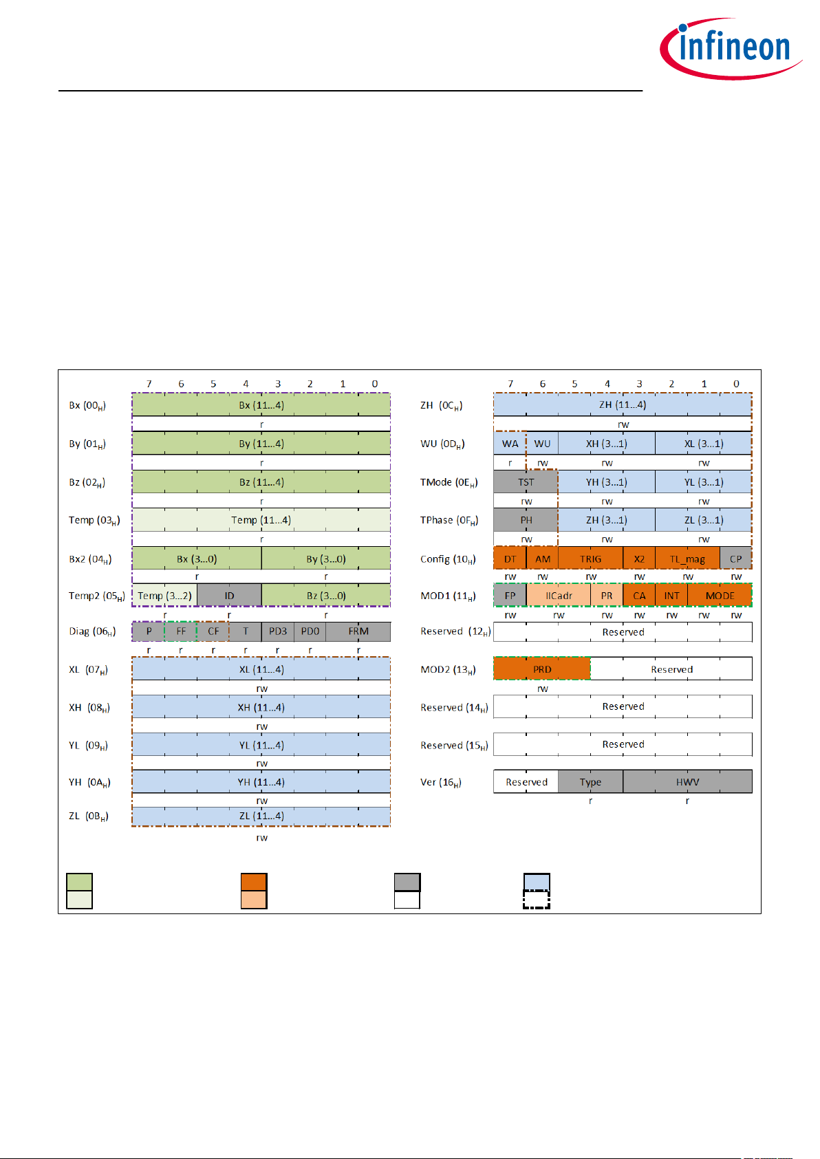
A bitmap overview is presented in Figure 1. Basically the following sections are available:
• measurement data (green bits in registers 00H till 05H)
• sensor status and diagnostics (grey bits in registers 05H, 06H, 0EH, 0FH, 10H and 11H)
• configuration parameters such as the power mode (orange bits in registers 10H, 11H and 13H)
• Wake Up values in registers (blue bits in registers 07H till 0FH)
Figure 1 TLE493D-P2B6 Bitmap
The diagnostic register 06H contains parity information as a diagnostic mechanism. The bitmap illustrates this
and marks the relationship of the sections to this flags with dierent colored lines/frames around the bit
contents.
Usermanual 4 Ver. 1.0
2020-12-11
Page 5
Usermanual TLE493D-P2B6
High Accuracy Low Power 3D Hall Sensor with I²C Interface
1 I2C Register
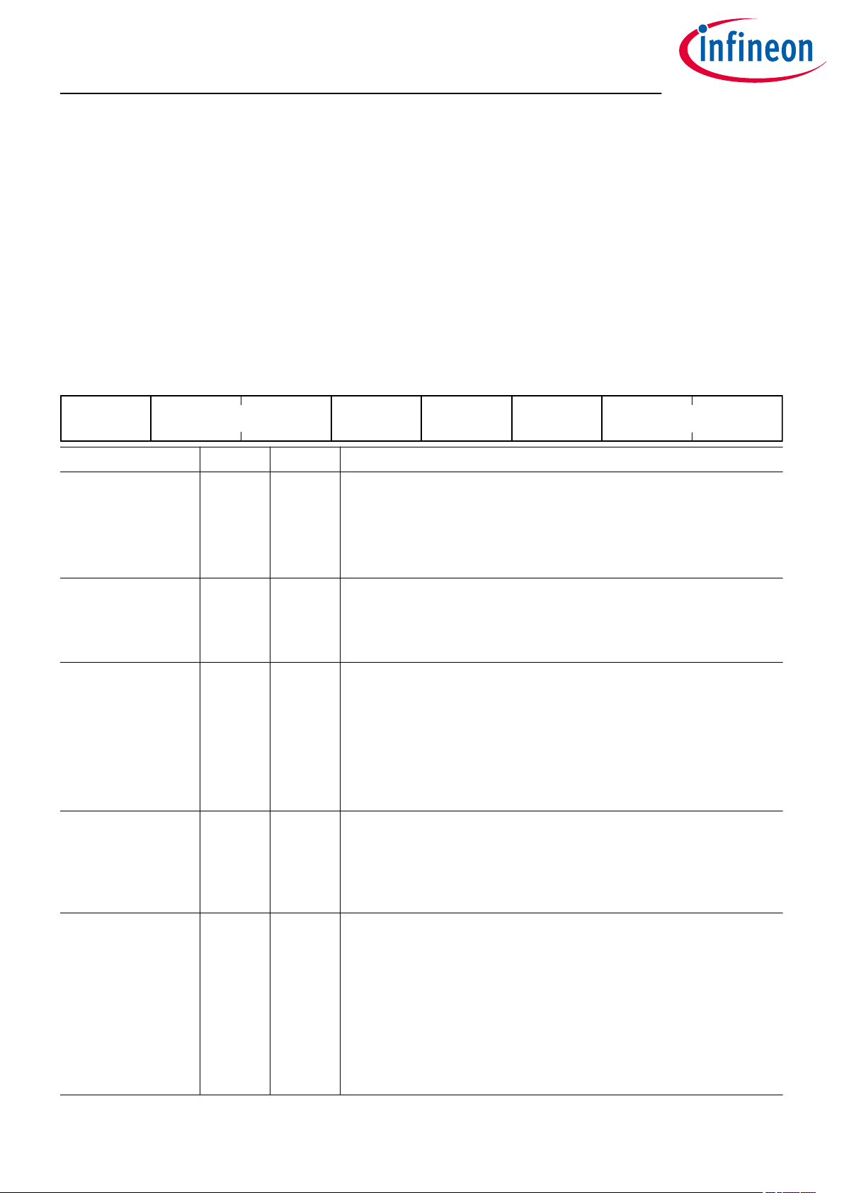
Table 1 Register overview
Register name Register long name Address
Bx, By and Bz Magnetic values MSBs 00H, 01H, 02
Temp Temperature value MSBs 03
Bx2 Magnetic values LSBs 04
Temp2 Temperature and magnetic LSBs and device address 05
Diag Sensor diagnostic and status register 06
H
H
H
H
XL, YL and ZL Wake Up lower threshold MSBs 07H, 09H, 0B
XH, YH and ZH Wake Up upper threshold MSBs 08H, 0AH, 0C
WU Wake Up enable and X thresholds LSBs 0D
TMode Test Mode and Wake Up Y thresholds LSBs 0E
TPhase Test Phase and Wake Up Z thresholds LSBs 0F
Config Configuration register 10
MOD1 Power mode, interrupt, address, parity 11
MOD2 Low Power Mode update rate 13
Ver Version register 16
H
H
H
H
H
H
H
1.2 Register description
H
H
H
The I2C registers can be read or written at any time. It is recommended to read measurement data in a
synchronized fashion, i.e. aer an interrupt pulse (/INT). This avoids reading inconsistent sensor or diagnostic
data, especially in fast mode. Additionally, several flags can be checked to ensure the register values are
consistent and the ADC was not running at the time of readout.
1.2.1 Bit types
The TLE493D-P2B6 contains read bits, write bits and reserved bits.
Table 2 Bit types
Abbreviation Function Description
r Read Read-only bits
rw Read Write Readable and writable bit
Reserved Bits that must keep the default values (read prior to write required)
1.2.2 Measurement data and registers combined in the I²C parity bit “P”
The I2C communication of the registers in this chapter is protected with the parity bit “P”, described in the Diag
register with the address 06H. See also Figure 1 - parity bits and related registers.
To make sure all data is consistent, the registers from 00H to 06H should be read with the same I2C command.
Otherwise, the sampled data (X, Y, Z, Temperature) may correspond to dierent conversion cycles.
Usermanual 5 Ver. 1.0
2020-12-11
Page 6
7
0
Bx, By and Bz (11...4)
7
0
Temp (11...4)
7
0
Bx (3...0)
By (3...0)
4 3
Usermanual TLE493D-P2B6
High Accuracy Low Power 3D Hall Sensor with I²C Interface
1 I2C Register
Magnetic values MSBs
Register names Address Reset Value
Bx, By and Bz 00H, 01H, 02
H
80
Field Bits Type Description
Bx, By and Bz 7:0 r Bx, By and Bz values
Signed value as two’s complement from the HALL probes in the
x, y and z-direction of the magnetic field. Contains the eight Most
Significant Bits. If Bz is deactivated the Bz value is the reset value.
Back to TLE493D-P2B6 Bitmap.
Temperature value MSBs
Register name Address Reset Value
Temp 03
H
80
Field Bits Type Description
H
H
Temp 7:0 r Temperature value
Signed value as two’s complement. If the temperature
measurement is deactivated, the Temp value is the reset value.
Back to TLE493D-P2B6 Bitmap.
Magnetic values LSBs
Register name Address Reset Value
Bx2 04
H
00
Field Bits Type Description
Bx 7:4 r Bx value
Signed value as two’s complement from the HALL probes in the xdirection of the magnetic field. Contains the four Least Significant
Bits.
By 3:0 r By value
Signed value as two’s complement from the HALL probes in the ydirection of the magnetic field. Contains the four Least Significant
Bits.
H
Back to TLE493D-P2B6 Bitmap.
Usermanual 6 Ver. 1.0
2020-12-11
Page 7
7
0
Bz (3...0)
4 3
Temp (3...2)
ID
6
5
Usermanual TLE493D-P2B6
High Accuracy Low Power 3D Hall Sensor with I²C Interface
1 I2C Register
Temperature and magnetic LSBs and device address
Register name Address Reset Value
Temp2 05
H
Field Bits Type Description
Temp 7:6 r Temperature value
Signed value as two’s complement. If the temperature
measurement is deactivated, the Temp value is the reset value.
ID 5:4 r ID
Readback of the sensor ID, from IICadr . µC shall verify the address
sent by the sensor. See Table 4 .
Bz 3:0 r Bz value
Signed value as two’s complement from the HALL probes in the zdirection of the magnetic field. Contains the four Least Significant
Bits. If Bz is deactivated the Bz value is 0H.
(Product Type A0) 00
(Product Type A1) 10
(Product Type A2) 20
(Product Type A3) 30
H
H
H
H
Back to TLE493D-P2B6 Bitmap.
Usermanual 7 Ver. 1.0
2020-12-11
Page 8
7
0
XL, YL and ZL (11...4)
7
0
XH, YH and ZH (11...4)
7
0
6
5 3
2
XL (3...1)XH (3...1)WUWA
Usermanual TLE493D-P2B6
High Accuracy Low Power 3D Hall Sensor with I²C Interface
1 I2C Register
1.2.3 Wake Up and registers combined in the I2C parity flag “CF"
The I2C communication of the registers in this chapter is protected by the parity bit CF, which is described in the
Diag register with the address 06H. See also Figure 1 - parity bits and related registers.
Wake Up lower threshold MSBs
Register names Address Reset Value
XL, YL and ZL 07H 09H 0B
H
80
Field Bits Type Description
XL, YL and ZL 7:0 rw Wake Up lower threshold
Defines the lower threshold MSBs of the magnetic field in the x, y
and z-direction at or below which the sensor enables the /INT, if
INT bit = 0B.
See Equation 2.
Back to TLE493D-P2B6 Bitmap.
Wake Up upper threshold MSBs
Register names Address Reset Value
XH, YH and ZH 08H 0AH 0C
H
7F
H
H
Field Bits Type Description
XH, YH and ZH 7:0 rw Wake Up upper threshold
Defines the upper threshold MSBs of the magnetic field in the x,
y and z direction at or above which the sensor enables the /INT, if
INT bit = 0B. See Equation 2.
Back to TLE493D-P2B6 Bitmap.
Wake Up enable and X thresholds LSBs
Register name Address Reset Value
WU 0D
Usermanual 8 Ver. 1.0
H
2020-12-11
38
H
Page 9
7
0
6
5 3
2
YL (3...1)YH (3...1)TST
Usermanual TLE493D-P2B6
High Accuracy Low Power 3D Hall Sensor with I²C Interface
1 I2C Register
Field Bits Type Description
WA 7 r Wake Up mode active
Flag that reports whether the Wake Up mode is disabled or
enabled.
If 0B the Wake Up mode is disabled.
If 1B the Wake Up mode is enabled.
This bit can be checked if the Wake Up function is disabled or
enabled. As long as the WA bit = 0B, the /INT will be asserted
according Table 5.
WU 6 rw Enables Wake Up mode
If 0B the Wake Up mode will be disabled.
If 1B the Wake Up mode will be enabled.
The following conditions must be fulfilled:
• Test modes must be disabled (T bit = 0B)
• CP parity bit (register 10H) must be odd
• Configuration parity must be flagged (CF bit = 1B)
Interrupts /INT will be sent when the measurement data is ≥ upper
or ≤ lower Wake Up threshold.
XH 5:3 rw Wake Up X upper threshold
Defines the upper threshold LSBs of the magnetic field in the
x-direction at or above the sensor enables the /INT, if INT bit = 0B.
See Equation 2.
XL 2:0 rw Wake Up X lower threshold
Defines the lower threshold LSBs of the magnetic field density in
the x-direction at or below the sensor enables the /INT, if INT bit =
0B. See Equation 2.
Back to TLE493D-P2B6 Bitmap.
Test Mode and Wake Up Y thresholds LSBs
Register name Address Reset Value
TMode 0E
H
Field Bits Type Description
TST 7:6 rw Test mode
Dierent test modes can be enabled, see Table 3:
If 00B no test active (normal sensor operation and T bit = 0B). In the
following test modes the T bit = 1B and the test result overwrites
the measurement data register:
If 01B Vhall/Vext test starts: measure the Hall bias voltage on all
Hall plates and VDD.
If 10B Spintest starts: the PH bits select the channel to diagnose
with the Spin-switch and Hall-oset test.
If 11B SAT test starts: a test of the whole digital path, generates
patterns, defined by the PH bits during conversion.
Usermanual 9 Ver. 1.0
2020-12-11
38
H
Page 10
7
0
6
5 3
2
ZL (3...1)ZH (3...1)PH
7
0
CP
6
5
4
3
2
1
TL_magX2AMDT TRIG
Usermanual TLE493D-P2B6
High Accuracy Low Power 3D Hall Sensor with I²C Interface
1 I2C Register
Field Bits Type Description
YH 5:3 rw Wake Up Y upper threshold
Defines the upper threshold LSBs of the magnetic field in the
y-direction at or above which the sensor enables the /INT, if INT bit
= 0B.
See Equation 2.
YL 2:0 rw Wake Up Y lower threshold
Defines the lower threshold LSBs of the magnetic field density in
the y-direction at or below which the sensor enables the /INT, if INT
bit = 0B. See Equation 2.
Back to TLE493D-P2B6 Bitmap.
Test Phase and Wake Up Z thresholds LSBs
Register name Address Reset Value
TPhase 0F
H
Field Bits Type Description
PH 7:6 rw Test phase selection
In the Spintest these bits define the channel. In the digital test,
specific patterns are defined. See Test phase selection Table 3.
The PH bits have no eect in the voltage measurement test (Vext)
and in normal operating mode TST bit=00B and T bit=0B).
See Equation 2.
ZH 5:3 rw Wake Up Z upper threshold
Defines the upper threshold LSBs of the magnetic field in the
z-direction at or above which the sensor enables the /INT, if INT bit
= 0B.
See Equation 2.
ZL 2:0 rw Wake Up Z lower threshold
Defines the lower threshold LSBs of the magnetic field density in
the z-direction at or below which the sensor enables the /INT, if INT
bit = 0B. See Equation 2.
38
H
Back to TLE493D-P2B6 Bitmap.
Configuration register
Register names Address Reset Value
Config 10
Usermanual 10 Ver. 1.0
H
2020-12-11
01
H
Page 11

Usermanual TLE493D-P2B6
High Accuracy Low Power 3D Hall Sensor with I²C Interface
1 I2C Register
Field Bits Type Description
DT 7 rw Disable Temperature
If 0B temperature measurement is enabled.
If 1B temperature measurement is disabled. This means the Bx, By
and Bz channels are measured. The Temp channel is disabled and
contains the reset value until a new conversion with Temp is done.
AM 6 rw X/Y Angular Measurement
If 0B the Bz measurement is enabled.
If 1B and DT bit = 1B: the Bz measurement is disabled. This means
the Bx and By channel is measured. The channels Bz and Temp
contain the reset values until a new conversion with Bz and Temp
is done
If 1B and DT bit = 0B: must not be used.
TRIG 5:4 rw Trigger options
If PR bit = 1B (1-byte read protocol), the TRIG bits define the trigger
mode of the device:
If 00B no ADC trigger on read
If 01B ADC trigger on read before first MSB.
If 1xB ADC trigger on read aer register 05H.
If PR bit = 0B these bits have no eect.
X2 3 rw Short range sensitivity
When this bit is set, the sensitivity of the Bx, By, and Bz ADCconversion is doubled by a longer ADC integration time. The Temp
result will not change, neither in sensitivity nor conversion time.
See Table 3.
TL_mag 2:1 rw Magnetic temperature compensation
There are two bits for setting the sensitivity over temperature of
the sensor to compensate a magnet temperature coeicient.
If 00B → TC0 (no compensation)
If 01B → TC
If 10B → TC
If 11B → TC
1
2
3
CP 0 rw Wake Up and configuration parity
The registers 07H through 10H (including 10H) without WA TST and
PH bit are odd parity protected with this bit. On startup or reset,
this parity is false and the CF bit in the status register 06H is
cleared. Thus the CP bit has to be corrected once aer startup or a
reset.
If this parity bit is incorrect during a write cycle, the Wake Up is
disabled.
Usermanual 11 Ver. 1.0
2020-12-11
Page 12
Usermanual TLE493D-P2B6
High Accuracy Low Power 3D Hall Sensor with I²C Interface
1 I2C Register
Table 3 Test mode interaction of TST, PH and X2 bits
TST bits PH bits X2 bit Bx (11...0) By (11...0) Bz (11...0) T (11...2)
00
00
01
10
10
10
10
11
11
11
11
11
11
11
11
B
B
B
B
B
B
B
B
B
B
B
B
B
B
B
don´t care 0
don´t care 1
B
B
don´t care don´t care Vhall X Vhall Y Vhall Z Voltage V
00
01
10
11
00
01
10
11
00
01
10
11
B
B
B
B
B
B
B
B
B
B
B
B
don´t care Spintest-Bx,
don´t care Spintest-By,
don´t care Spintest-Bz,
don´t care Spintest-T,
0
B
0
B
0
B
0
B
1
B
1
B
1
B
1
B
Bx full-range By full-range Bz full-range T full-range
Bx short-range By short-range Bz short-range T full-range
DD
spin-0 disabled
spin-0 disabled
spin-0 disabled
setting1
7F9
H
806
H
7FF
H
800
H
7FF
H
800
H
7FF
H
800
H
Spintest-Bx,
spin-1 disabled
Spintest-By,
spin-1 disabled
Spintest-Bz,
spin-1 disabled
Spintest-T,
setting2
806
H
7F9
H
800
H
7FF
H
800
H
7FF
H
800
H
7FF
H
Spintest-Bx,
spin-2 disabled
Spintest By,
spin-2 disabled
Spintest-Bz,
spin-2 disabled
Spintest-T,
setting2
7FF
H
800
H
7F9
H
806
H
7FF
H
800
H
7FF
H
800
H
Spintest-Bx,
spin-3 disabled
Spintest By,
spin-3 disabled
Spintest-Bz,
spin-3 disabled
Spintest-T,
setting1
200
H
1FF
H
201
H
1FE
H
200
H
1FF
H
201
H
1FE
H
Back to TLE493D-P2B6 Bitmap.
Usermanual 12 Ver. 1.0
2020-12-11
Page 13
7
0
FP
6 3 2 1
PR INT MODE
5 4
IICadr CA
Usermanual TLE493D-P2B6
High Accuracy Low Power 3D Hall Sensor with I²C Interface
1 I2C Register
1.2.4 Mode registers combined in the I²C parity flag “FF”
The I²C communication of the registers in this chapter is protected with the parity bit “FF”, described in the Diag
register with the address 06H. See also Figure 1 - parity bits and related registers.
Power mode, interrupt, address, parity
Register name Address Reset Value
MOD1 11
H
Field Bits Type Description
FP 7 rw Fuse parity
The registers 11H and 13H (bits 7:5) are odd parity protected with
this bit.
If this parity bit is incorrect please see FF bit.
To exit this state a sensor reset is necessary.
IICadr 6:5 rw I²C address
Bits can be set to 00B, 01B, 10B or 11B to define the slave address in
bus configuration.
See Table 4 and data sheet.
PR 4 rw I²C 1-byte or 2-byte read protocol
If 0B this is the 2-byte read protocol:
<start> <I²Cadr.> <reg.adr.> <data of reg.adr.> <data of reg.adr.+1>
…. <stop>
If 1B this is the 1-byte read protocol:
<start> <I²Cadr.> <data of reg.00H> <data of reg.01H> …. <stop>
See I²C read commands
(Product Type A0) 80
(Product Type A1) 20
(Product Type A2) 40
(Product Type A3) E0
H
H
H
H
CA 3 rw Collision avoidance
Clock stretching only in master-controlled and low-power mode,
not in fast mode.
The CA bit interacts with the INT bit, see Table 5 and Collision
avoidance and clock stretching.
INT 2 rw Interrupt enabled
If 1B /INT disabled
If 0B /INT enabled: Aer a completed measurement and ADC-
conversion, an /INT pulse will be generated.
For bus configurations /INT timing constraints between I²C data
transfers and interrupt pulses must be monitored and aligned.
Enabled Wake Up mode or Collision avoidance (CA bit = 0B and
INT bit = 0B) may suppress the /INT pulse.
The INT bit interacts with the CA bit, see Table 5 .
Usermanual 13 Ver. 1.0
2020-12-11
Page 14

Usermanual TLE493D-P2B6
High Accuracy Low Power 3D Hall Sensor with I²C Interface
1 I2C Register
Field Bits Type Description
MODE 1:0 rw Power mode
If 00B Low Power Mode:
Cyclic measurements and ADC-conversions with a update rate,
defined in the PRD registers. “No ADC trigger” must be used, see
Table 6 and TRIG.
If 01B Master Controlled Mode (Power Down mode):
Measurement triggering depends on the PR bit and is possible with
I²C sub address byte (see Table 6) or TRIG bits.
If 10B is reserved and must not be used.
If 11B Fast Mode:
The measurements and ADC-conversions are running
continuously. It is recommended to set INT = 0B and use a I²C clock
speed ≥ 800 kHz.
Back to TLE493D-P2B6 Bitmap.
Table 4 Device address overview
The addresses are selected to ensure a minimum Hamming distance of 4 between them.
Product
Type
Default address
write
A0 6A
A1 44
A2 F0
A3 88
1)
Default address
read
H
H
H
H
6B
45
F1
89
H
H
H
H
1)
IICadr (bit-6) IICadr (bit-5) ID (bit-5) ID (bit-4)
0
B
0
B
1
B
1
B
0
B
1
B
0
B
1
B
0
B
0
B
1
B
1
B
Table 5 /INT (interrupt), collision avoidance and clock stretching configuration
CA INT Configuration
0
B
0
B
/INT and collision avoidance enabled
Clock stretching disabled
0
B
1
B
/INT and collision avoidance disabled
Clock stretching enabled
This configuration must not be used:
• in fast mode
• with the “read” trigger-bits (7:5) = 010B or 011B (see Table 6)
• with the trigger option TRIG bit = 01B.
0
B
1
B
0
B
1
B
1
B
0
B
/INT enabled and collision avoidance disabled
Clock stretching disabled
1
B
1
B
/INT and collision avoidance disabled
Clock stretching disabled
1
See data sheet ordering information
Usermanual 14 Ver. 1.0
2020-12-11
Page 15

7
0
PRD
Reserved
4
5
7
0
FRM
6
5
4
3
2
1
PD0PD3TCFFFP
Usermanual TLE493D-P2B6
High Accuracy Low Power 3D Hall Sensor with I²C Interface
1 I2C Register
Low Power Mode update rate
Register name Address Reset Value
MOD2 13
H
Field Bits Type Description
PRD 7:5 rw Update rate settings
If 000B typ. update frequency f
If 001B typ. update frequency f
If 010B typ. update frequency f
If 011B typ. update frequency f
If 100B typ. update frequency f
If 101B typ. update frequency f
If 110B typ. update frequency f
If 111B typ. update frequency f
Reserved 4:0 rw Factory settings
Do not modify, read before write required.
Back to TLE493D-P2B6 Bitmap.
1.2.5 Diagnostic, status and version registers
Update
Update
Update
Update
Update
Update
Update
Update
≈ 770 Hz.
≈ 97 Hz.
≈ 24 Hz.
≈ 12 Hz.
≈ 6 Hz.
≈ 3 Hz.
≈ 0.4 Hz.
≈ 0.05 Hz.
(bits 7:5) 000
B
The device provides diagnostic and status information in register 06H and version information in register 16H.
Sensor diagnostic and status register
Register name Address Reset Value
Diag 06
H
60
Field Bits Type Description
P 7 r Bus parity
This bit adds up to an odd parity of the registers 00H through
05H (including 05H), described in Measurement data and registers
combined in the I²C parity bit “P”.
The parity bit is generated during the I²C readout. The address
byte, register byte and acknowledge bits are not included in the
parity sum.
If the parity calculated by the microcontroller aer I²C reads is
incorrect, these values must be treated as invalid.
H
Usermanual 15 Ver. 1.0
2020-12-11
Page 16

Usermanual TLE493D-P2B6
High Accuracy Low Power 3D Hall Sensor with I²C Interface
1 I2C Register
Field Bits Type Description
FF 6 r Fuse parity flag
Provides a flag from the internal fuse parity check of registers 11
to 15H. This parity check includes the FP bit.
If 1B parity is OK.
If 0B the parity is not correct. The sensor must be considered
defective and must no longer be used. A sensor with an invalid fuse
parity disconnects its SDA. It will automatically go to low-power
mode and only uses the /INT signal to communicate the error
(collision avoidance is enabled).
CF 5 r Wake Up and configuration parity flag
Provides a flag from the internal configuration and Wake Up parity
check of registers 07H through 10H (including 10H) without WA TST
and PH bit. This parity check includes the CP bit.
If 1B parity is OK.
If 0B parity is not OK, or aer startup or aer reset the CP bit is
false to indicate a reset of all registers. Thus the CP bit has to be
corrected once aer startup or a reset.
H
T 4 r Test mode
If 1B test mode is enabled. Data in registers 00H till 05H are either
test results or - aer a “ADC restart” - invalid measurement data.
If 0B test mode is disabled, valid measurement data available.
PD3 3 r Power-down flag 3
If 1B ADC-conversion of Temp is completed and valid measurement
data can be read out. Thus it must be 1B at readout.
If 0B ADC-conversion of Temp is running and read measurement
data are invalid. Any readout with PD3 bit = 0B should be
considered invalid.
At startup, this is 0B until one ADC conversion has been performed.
The value then changes to 1B.
PD0 2 r Power-down flag 0
If 1B the ADC conversion of Bx is completed and valid measurement
data can be read out. Thus it must be 1B at readout.
If 0B the ADC conversion of Bx is running and read measurement
data are invalid. Any readout with PD0 bit = 0B should be
considered invalid.
At startup, this is 0B until one ADC conversion has been performed.
The value then changes to 1B.
FRM 1:0 r Frame counter
Increments at every updated ADC-conversion, once a X/Y/Z/T or
X/Y/Z or X/Y conversion is completed and the new measurement
data have been stored in the registers 00H till 05H.
The microcontroller shall check if bits change in consecutive
conversion runs.
Back to TLE493D-P2B6 Bitmap.
Usermanual 16 Ver. 1.0
2020-12-11
Page 17

7
0
Reserved
HWV
4 3
TYPE
6
5
Usermanual TLE493D-P2B6
High Accuracy Low Power 3D Hall Sensor with I²C Interface
1 I2C Register
Version register
Register name Address Reset Value
Ver 16
H
Field Bits Type Description
Reserved 7:6 r Factory settings
TYPE 5:4 r Chip feature
If 00B, 10B or 01B: device with Wake Up feature.
HWV 3:0 r Hardware revision
If 9H it is the B21 design step.
Back to TLE493D-P2B6 Bitmap.
C9H, D9H or E9
H
Usermanual 17 Ver. 1.0
2020-12-11
Page 18

Usermanual TLE493D-P2B6
High Accuracy Low Power 3D Hall Sensor with I²C Interface
2 I²C Interface
2 I²C Interface
The TLE493D-P2B6 uses Inter-Integrated Circuit (I²C) as the communication interface with the microcontroller.
The I²C interface has three main functions:
• Sensor configuration
• Transmit measurement data
• Interrupt handling
This sensor provides two I²C read protocols:
• 16-bit read frame (µC is driving data), so called 2-byte read command.
• 8-bit read frame (µC is driving data), so called 1-byte read command.
2.1 I²C protocol description
The TLE493D-P2B6 provides one I²C write protocol, based on 2 bytes and two I²C read protocols. Default is the
2-byte read protocol. With the PR bit it can be selected, if the 1-byte read protocol or the 2-byte read protocol is
used.
2.1.1 General description
• The interface conforms to the I2C fast mode specification (400kBit/sec max.), but can be driven faster
according to the data sheet.
• The TLE493D-P2B6 does not support “repeated starts”. Each addressing requires a start condition.
• The interface can be accessed in any power mode.
• The data transmission order is Most Significant Bit (MSB) first, Least Significant Bit (LSB) last.
• A I²C communication is always initiated with a start condition and concluded with a stop condition by the
master (microcontroller). During a start or stop condition the SCL line must stay “high” and the SDA line
must change its state: SDA line falling = start condition and SDA line rising = stop condition.
• Bit transfer occur when the SCL line is “high”.
• Each byte is followed by one ACK bit. The ACK bit is always generated by the recipient of each data byte.
- If no error occurs during the data transfer, the ACK bit will be set to “low”.
- If an error occurs during the data transfer, the ACK bit will be set to “high”.
- If the communication is finished (before the Stop condition), the ACK bit must be set to “high”.
2.1.2 I²C write command
Write I²C communication description:
• The purpose of the sensor address is to identify the sensor with which communication should occur. The
sensor address byte is required independently of the number of sensors connected to the microcontroller.
• The register address identifies the register in the bitmap (according to Figure 1) with which the first data
byte will be written.
• Data bytes are transmitted as long as the SCL line generates pulses. Each additional data byte increments
the register address until the stop condition occurs.
• Bytes transmitted beyond the register address frame are ignored and the corresponding ACK bit is sent
“high”, indicating an error.
The I2C write communication frame consists of:
• The start condition.
• The sensor address, according to Table 4.
• Write command bit = “low” (read = “high”).
Usermanual 18 Ver. 1.0
2020-12-11
Page 19

SCL
SDA
I2C master is driving data (µC) I2C slave is driving data (sensor)
ACK ACK ACKWrite dataSensor address
Register
address
Trigger
bits
Usermanual TLE493D-P2B6
High Accuracy Low Power 3D Hall Sensor with I²C Interface
2 I²C Interface
• Acknowledge ACK.
• Trigger bits, according to Table 6.
• The register address, according to Figure 1.
• Acknowledge ACK.
• Writing of one or several bytes to the sensor, each byte followed by an acknowledge ACK.
• The stop condition.
Figure 2 General I²C write frame format: Write data from microcontroller to sensor
Trigger bits in the I²C protocol
The trigger bits are used in Power Down Mode. The Power Down Mode is used in the Master Controlled Mode,
when no measurement is running. Thus the trigger bits are relevant for the Master Controlled Mode as well.
For a more silent measurement environment it is recommended to separate the measurement and the
communication as much as possible, by using the trigger bits = 001B or trigger bits = 100B and communicate
between two measurements with reduced overlap of measurement and communication.
Table 6 I2C trigger bits
Read/Write
Trigger-bit 7 Trigger-bit 6 Trigger-bit 5 Trigger command
command
0
B
0
B
0
B
0
B
0
B
0
B
0
B
0
B
1
B
1
B
1
B
1
B
1
B
1
B
1
B
1
B
0
B
0
B
0
B
0
B
1
B
1
B
1
B
1
B
0
B
0
B
0
B
0
B
1
B
1
B
1
B
1
B
0
B
0
B
1
B
1
B
0
B
0
B
1
B
1
B
0
B
0
B
1
B
1
B
0
B
0
B
1
B
1
B
0
B
1
B
0
B
1
B
0
B
1
B
0
B
1
B
0
B
1
B
0
B
1
B
0
B
1
B
0
B
1
B
no ADC trigger
ADC trigger aer write frame is finished, Figure 4
no ADC trigger
ADC trigger aer write frame is finished, Figure 4
no ADC trigger
ADC trigger aer write frame is finished, Figure 4
no ADC trigger
must not be used
no ADC trigger
no ADC trigger
ADC trigger before first MSB, Figure 3
ADC trigger before first MSB, Figure 3
ADC trigger aer register 05H, Figure 5
ADC trigger aer register 05H, Figure 5
ADC trigger aer register 05H, Figure 5
must not be used
Usermanual 19 Ver. 1.0
2020-12-11
Page 20

SCL
SDA
I2C master is driving data (µC) I2C slave is driving data (sensor)
ACK
Read data
Sensor address
Register
address
ADC
ACK ACK
ADC conversion
SCL
SDA
I2C master is driving data (µC) I2C slave is driving data (sensor)
ACK
Write data
Sensor address
Register
address
ADC
ACK ACK
ADC conversion
SCL
SDA
I2C master is driving data (µC) I2C slave is driving data (sensor)
ACK
Read data
Sensor address
Register
address
ADC
ACK ACK
ADC conversion
ACK
Read data 06
H
Read data 05
H
ACK
Usermanual TLE493D-P2B6
High Accuracy Low Power 3D Hall Sensor with I²C Interface
2 I²C Interface
Figure 3 ADC trigger before sending first MSB of data registers, I²C trigger bits 010
Figure 4 ADC trigger aer write frame is finished, I²C trigger bits 001
B
B
Figure 5 ADC trigger aer register 05H, I²C trigger bits 100
Usermanual 20 Ver. 1.0
B
2020-12-11
Page 21

0 1 1 0 1 0 1 0 0 0 0 0 1 0 0 0 1 0 x 0 0 0 0 1 0 1 0
SCL
SDA
I2C master is driving data (µC) I2C slave is driving data (sensor)
ACK ACK ACK
Usermanual TLE493D-P2B6
High Accuracy Low Power 3D Hall Sensor with I²C Interface
2 I²C Interface
Example I²C write communication
An example of a write communication is provided in Figure 6.
In this example the sensor with the address 6AH / 6BH (see Table 4) should be configured for:
• Master Controlled Mode
• /INT disabled
• Clock stretching enabled
• No trigger of a measurement
• Other settings should be kept as is
Implementation:
• The microcontroller generates a start condition
• Configuration changes can only be performed with a write command. The address for write operation of
this sensor is 6AH = 01101010
• If the sensor detects no error, the ACK = 0B is transmitted back to the microcontroller
• No measurement is performed if the trigger bits = 000
• The register to change the required settings is 11H according the bitmap Figure 1 = 10001
• If the sensor detects no error, the ACK = 0B is transmitted back to the microcontroller
• The parity bit “FP” is the odd parity of the registers 11H and 13H (bits 7:5), see FP register, thus it is not
possible to quantify it in this example
• The sensor address should not be changed, i.e. the sensor address 6AH / 6BH should be kept. Thus the
IICadr bits = 00B, see IICadr registers
• The 2-byte protocol should be kept as is. Thus the PR bit = 0
• In order to enable clock stretching and disable /INT the CA bit must be set to 0B and the INT bit must be set
to 1B (see Table 5)
• To use the Master Controlled Mode the MODE bits must be set to 01
• If the sensor detects no error the ACK = 0B is transmitted back to the microcontroller
• The microcontroller generates the stop condition
B
B
B
B
B
Figure 6 Example I²C frame format 2-byte: Write data from microcontroller to sensor
Usermanual 21 Ver. 1.0
2020-12-11
Page 22

SCL
SDA
I2C master is driving data (µC) I2C slave is driving data (sensor)
ACK ACK
ACK
Register
address
Read dataSensor address
Trigger
bits
Usermanual TLE493D-P2B6
High Accuracy Low Power 3D Hall Sensor with I²C Interface
2 I²C Interface
2.1.3 I²C read commands
Read I²C communication description:
• The purpose of the sensor address is to identify the sensor with which communication should occur. The
sensor address byte is required independently of the number of sensors connected to the microcontroller.
• Only available in the 2-byte read command: The register address identifies the register in the bitmap
(according Figure 1) from which the first data byte will be read. In the 1-byte read command the read out
starts always at the register address 00H.
• As many data bytes will be transferred as long as pulses are generated by the SCL line. Each additional data
byte increments the register address. Until the stop condition occurs.
• If bytes are read beyond the register address frame the sensor keeps the SDA = 1B.
• If the microcontroller reads data and does not acknowledge the sensor data (ACK = 1B) the sensor keeps the
SDA = 1B until the next stop condition.
2.1.3.1 2-byte read command
The I²C read communication frame consists of:
• The start condition
• The sensor address, according to Table 4
• Read command bit = “high” (write = “low”)
• Acknowledge ACK
• Trigger bits, according to Table 6
• The register address, according to Figure 1
• Acknowledge ACK
• Reading of one or several bytes from the sensor, each byte followed by an acknowledge ACK
• The stop condition
Figure 7 General I²C frame format 2-byte: Read data from sensor to microcontroller
2.1.3.2 1-byte read command
The 1-byte read mode can be entered, by configuring the PR bit with an write communication. For example with
the write cycle:
• start condition
• 6AH (sensor address)
• 11H (register address)
• XXX1 XXXXB (PR bit = 1B)
• stop condition
Usermanual 22 Ver. 1.0
2020-12-11
Page 23

SCL
SDA
I2C master is driving data (µC) I2C slave is driving data (sensor)
ACK
ACKRead dataSensor address
1 1 1 1 0 0 0 1 0 0 1
SCL
SDA
I2C master is driving data (µC) I2C slave is driving data (sensor)
ACK ACK NACK
0
ACKRead data reg. 00
H
Read data reg. 06
H
Usermanual TLE493D-P2B6
High Accuracy Low Power 3D Hall Sensor with I²C Interface
2 I²C Interface
The I²C communication frame consists of:
• The start condition
• The sensor address, according to Table 4
• Read command bit = “high” (write = “low”)
• Acknowledge ACK
• Reading of one or several bytes from the sensor, each byte followed by an acknowledge ACK
• The stop condition
Figure 8 General I²C frame format 1-byte: Read data from sensor to microcontroller
Example I²C 1-byte read communication
An example of a read communication is provided in Figure 9.
In this example, the sensor with the address F0H / F1H (see Table 4) should read out the measurement values,
registers 00H - 05H and the diagnostic register 06H:
Implementation:
• The microcontroller generates a start condition
• The address for read operation of this sensor is F1H = 11110001B. This address value must be transmitted by
the microcontroller to the sensor
• If the sensor detects no error, the ACK = 0B is transmitted back to the microcontroller
• The microcontroller must go on clocking the SCL line
• The sensor transmits 8 data bits of register 00H to the microcontroller
• If the microcontroller detects no error the ACK = 0B is transmitted back to the sensor
• The microcontroller must go on clocking the SCL line
• The sensor transmits 8 data bits of register 01H to the microcontroller
• ...
• Aer transmitting the register 06H the microcontroller transmits a NACK
• The microcontroller generates the stop condition
Figure 9 Example I²C frame format 1-byte: Read data from sensor to microcontroller
Usermanual 23 Ver. 1.0
2020-12-11
Page 24

1 1 1 1 0 0 0 1
SCL
SDA
I2C master is driving data (µC) I2C slave is driving data (sensor)
ADC
conversion
Bz T
0
ACK Read data reg. 00
H
/INT
Corrupt data
1 1 1 1 0 0 0 1
SCL
SDA
I2C master is driving data (µC) I2C slave is driving data (sensor)
ADC
conversion
Bz T
0 0 1
ACK ACK NACK
0
ACK
Read data reg. 00
H
Read data reg. 06
H
/INT
omitted
Usermanual TLE493D-P2B6
High Accuracy Low Power 3D Hall Sensor with I²C Interface
2 I²C Interface
2.2 Collision avoidance and clock stretching
Using the configuration bits CA and INT, collision avoidance and clock stretching can be configured, see. An
overview is given in Table 5. An example without collision avoidance and clock stretching is shown in Figure 10.
In this example:
• The sensor interrupt disturbs the I²C clock, causing an additional SCL pulse which shis the data read out
by one bit
• The data read out starts when the ADC conversion is running
Figure 10 Example without collision avoidance CA bit =1B and INT bit = 0
B
2.2.1 Collision avoidance (CA bit = 0B and INT bit = 0B)
In a bus configuration combined with an activated interrupt signal /INT it must be assured, that during any
communication no interrupt /INT occurs. With collision avoidance enabled, the sensor monitors for any start/
stop condition, even if it does not detect a valid bus address. The interrupt signal /INT is omitted whenever
a start condition is detected, as shown in Figure 11, in contrast to Figure 10. Only aer a stop condition is
detected, the interrupt signal /INT is generated by the sensor.
It is strongly recommended to use the collision avoidance feature whenever the interrupt signal /INT is used.
Figure 11 Example with collision avoidance CA bit =0B and INT bit = 0
Usermanual 24 Ver. 1.0
B
2020-12-11
Page 25

Usermanual TLE493D-P2B6
High Accuracy Low Power 3D Hall Sensor with I²C Interface
2 I²C Interface
2.2.2 Clock stretching (CA bit = 0B and INT bit = 1B)
With the clock stretching feature, the data read out starts aer the ADC conversion is finished. Thus it can be
avoided that during an ADC conversion old or corrupted measurement results are read out, which may occur
when the ADC is writing to a register while this is being read out by the microcontroller. The clock stretching
feature is shown in Figure 12 in combination with a 1-byte read command. Clock stretching can also be used
with a 2-byte read command.
The sensor pulls the SCL line to low during the following situation:
• An ADC conversion is in progress
• The sensor is addressed for register read (writes are never aected by clock stretching)
• The sensor is about to transmit the valid ACK in response to the I²C addressing of the microcontroller
ADC
conversion
Start condition
SDA
1 1 1 1 0 0 0 1 0
SCL
I
2
C master is driving data (µC)
By Bz T
(read)
H
Sensor address
F1
Read command
C l o c k s t r e t c h i n g
2
I
ACK
Read data reg. 00
0
C slave is driving data (sensor)
Figure 12 Example with clock stretching CA bit =0B and INT bit = 1
01
B
Read data reg.
H
… 06
ACK
H
Stop condition
H
NACK
1
Usermanual 25 Ver. 1.0
2020-12-11
Page 26

Usermanual TLE493D-P2B6
High Accuracy Low Power 3D Hall Sensor with I²C Interface
2 I²C Interface
2.3 Sensor reset by I²C
If the microcontroller is reset, the communication with the sensor may be corrupted, possibly causing the
sensor to enter an incorrect state. The sensor can be reset via the I²C interface by sending the following
command sequence from the microcontroller to the sensor:
• Start condition
• Sending FF
• Stop condition
• Start condition
• Sending FF
• Stop condition
• Start condition
• Sending 00
• Stop condition
• Start condition
• Sending 00
• Stop condition
• 30 µs delay
Aer a reset, the sensor must be reconfigured to the desired settings. The reset sequence uses twice the
identical data to assure a proper reset, even when an unexpected /INT pulse occurs.
Spikes can be interpreted as bus signals causing an action. For example when the collision avoidance feature
is active and if the SDA line spikes together with SCL line this could be interpreted as start condition, blocking
further /INT pulses until a stop condition appears on the bus. In such a case the sensor must be reset in order to
initialize it. If the sensor does not respond aer the reset, it must be considered defective.
Such spikes may occur as the sensor powers up. Because of this we recommend to using the reset sequence
aer each power up before configuring the sensor.
If the microcontroller resets during an ongoing I²C communication, the SDA line could get stuck low. This would
block the I²C bus and is a well-known limitation of the I²C interface. To recover from this situation please use the
reset sequence described in this chapter.
H
H
H
H
Usermanual 26 Ver. 1.0
2020-12-11
Page 27

system init /INT handler
I²C: reset sensor
S FFH P, S FFH P,
S 00H P, S 00H P
I²C: write sensor
configuration
init I²C peripheral
configure interrupt
and enable /INT pin
wait for /INT goes
high again
disable /INT pin
I²C: read sensor data
and diagnosis
enable /INT pin
return
I²C read
successful?
/INT pulse
from sensor
application main
loop, takes sensor
data and errors for
processing
Valid sensor
data?
handle I²C peripheral
(reconfiguration, …)
flag sensor error
no
flag new sensor data
no
Evaluate diagnosis
information
yes
yes
serious error
situation?
yes: restart
no
Delay = 30µs
Usermanual TLE493D-P2B6
High Accuracy Low Power 3D Hall Sensor with I²C Interface
2 I²C Interface
2.4 Sensor Initialization and Readout example
To ensure that both the microcontroller and the sensor are synchronized and properly initialized, it is
recommended to apply the I²C reset and upload the fuse register settings each time the microcontroller is
reset, see Figure 13.
Figure 13 Microcontroller soware flowchart for TLE493D-P2B6
Usermanual 27 Ver. 1.0
2020-12-11
Page 28

Usermanual TLE493D-P2B6
High Accuracy Low Power 3D Hall Sensor with I²C Interface
2 I²C Interface
2.5 Loss of VDD impact on I²C bus
If the SDA or SCL line is pulled “low” and the sensor is disconnected from the VDD supply line, the aected I²C
line will most likely get a stuck in the Low state and will interfere with the communication on the bus.
Power supply loss
V
DD
Sensor
1
TLE493D-
P2B6
I²C bus
Sensor
n
I²C bus can
be disturbed
Microcontroller
Figure 14 Example of I²C bus and a TLE493D-P2B6 with disconnected V
When VDD is pulled to GND the SDA and SCL line will not disturb the bus.
DD
Usermanual 28 Ver. 1.0
2020-12-11
Page 29

t
/INT
Measurement and
ADC sampling
B-field (X,Y or Z)
Wake Up
upper threshold
Wake Up
lower threshold
Wake Up causes
the external µC
to update the
levels
f
Update
1
B
X,Y,Z
t
Usermanual TLE493D-P2B6
High Accuracy Low Power 3D Hall Sensor with I²C Interface
3 Wake Up mode
3 Wake Up mode
The Wake Up mode (or short WU mode) is intended to be used together with the automated sensor modes (e.g.
Low Power mode or Fast mode). In principle, it works with the Master Controlled mode as well, but it might not
really be useful there because a controlled trigger usually implies the need to acquire a new measurement.
This WU mode can be used to allow the sensor to continue making magnetic field measurements while the µC
is in the power-down state, which means the microcontroller will only consume power and access the sensor
if relevant measurement data is available. This can be done either by using static thresholds (for example for
applications where only movements of magnets away from a default position are relevant) or by using dynamic
thresholds (where any movement over a specific uncertainty limit should be detected once). The figure below
illustrates these two cases.
Figure 15 Static or Dynamic Wake Up Threshold Operation of the TLE493D-P2B6
This dynamic WU mode operation oers another option which is particularly useful in Fast mode with limited
I²C bus capabilities and/or low bit rates. In this case, the WU mode can act as a “data filter” to reduce the
bus load by preventing sensor data from being read that does not change significantly. So due to an interrupt,
the new WU levels are adapted to the actual value read (for each X, Y, Z channel individually). This provides
low latencies for detecting changes but reduces interrupts caused by similar values. If the collision avoidance
feature is also used, the readout may take even longer than one conversion time (but this readout speed adds
to the overall signal latency as well). As the thresholds also need to be set, a complete data read and set of
new WU thresholds is not even feasible with the fastest specified bit rate within one sensor sample time in Fast
mode.
The next figure illustrates this more clearly:
Usermanual 29 Ver. 1.0
2020-12-11
Page 30

t
t
the /INT pulses are suppressed
as communication is ongoing
Fast Mode
t
read
ADC
set
WU
read
ADC
set
WU
SCL
/INT
B
X,Y,Z
B-field (X,Y or Z)
Wake Up causes
the external µC to
update the levels
SDA
read
ADC
set
WU
read
ADC
set
WU
„Wake Up upper threshold“D > „Wake Up lower threshold“
D
„Wake Up upper threshold“D - „Wake Up lower threshold“D < 2048DLSB
12
Usermanual TLE493D-P2B6
High Accuracy Low Power 3D Hall Sensor with I²C Interface
3 Wake Up mode
Figure 16 Dynamic Wake Up Threshold Operation of the TLE493D-P2B6 for Bandwidth Reduction
To sum this up, we can state that this dynamic WU mode operation together with the Fast mode set allows
detecting and reading significant value changes with low latency, even if the bit rate of the I²C cannot be set fast
enough to read the data for each set of sensor data generated.
3.1 Wake Up activation
The Wake Up function can be activated with the WU bit and by modifying at least one of the Wake Up threshold
registers of address 07H to 0FH, see Configuration registers combined in the I²C parity flag “CF”.
Please note that the Wake Up registers cover bit 11 to bit 1. Bit 0 is not accessible, but internally set with 0B to
get a 12-bit value, for comparison with the 12-bit magnetic field value registers Bx, By and Bz.
3.2 Wake Up constraints
The Wake Up threshold range disabling /INT pulses between upper threshold and lower threshold is limited to a
window of the half output range.
This window itself can be moved inside the full output range, as illustrated in Figure 17.
Equation 1
Equation 2
Usermanual 30 Ver. 1.0
2020-12-11
Page 31

+2047 LSB12 ADC upper limit Bx, By, Bz
-2048 LSB12 ADC lower limit Bx, By, Bz
0
/INT disabled
/INT disabled
/INT disabled
/INT enabled
/INT enabled
/INT
enabled
/INT enabled
/INT disable range
can be decreased, but must
not be increased.
Usermanual TLE493D-P2B6
High Accuracy Low Power 3D Hall Sensor with I²C Interface
3 Wake Up mode
Figure 17 Wake Up enable and disable range examples
3.3 Wake Up in combination with the angular mode
In angular mode, see DT and AM bit, the
• “Wake Up Y upper threshold” must be written to the registers 0CH and 0FH (5 ... 3)(ZH in Figure 1)
• “Wake Up Y lower threshold” must be written to the registers 0BH and 0FH (3 ... 1)(ZL in Figure 1)
Usermanual 31 Ver. 1.0
2020-12-11
Page 32

Usermanual TLE493D-P2B6
High Accuracy Low Power 3D Hall Sensor with I²C Interface
4 Diagnostic and tests
4 Diagnostic and tests
The sensor TLE493D-P2B6 provides diagnostic functions and test functions:
• Diagnostic functions:
These functions are running in the background, providing results, which can be checked by the
microcontroller for the verification of the measurement results.
• Test functions:
These functions are only executed by the sensor following a request by the microcontroller. The test
functions provides test values instead of measurement values, which can be used to check if the sensor is
working properly.
4.1 Diagnostic functions
To ensure the integrity of received data the following diagnostic functions are available.
4.1.1 Parity bits and parity flags
Parity bits:
• FP (mode parity bit)
• CP (Wake Up and configuration parity bit)
• P (bus parity bit)
Parity flags:
• FF (mode parity flag)
• CF (Wake up and configuration parity flag)
4.1.2 Test mode
The device is in test mode, this is indicated by the T register (Diag register 06H bit 4).
4.1.3 Power-down flags
During measurements and during ADC conversion, the sensor monitors if the supply voltage is correct and if the
conversion is finished. This is indicated by the PD3 and PD0 registers.
4.1.4 Frame counter
The frame counter FRM register is incremented by one when a conversion is completed.
4.1.5 Device address
The TLE493D-P2B6 can be ordered with dierent default addresses. This device address can be read out with
the IICadr registers.
4.2 Test functions
The TLE493D-P2B6 includes three test functions which can be activated by the microcontroller, using the TST
registers in combination with the PH registers:
• Vhall/Vext test: checks the whole signal path from sensor to microcontroller
• Spintest: checks all Spin-switches, the Hall-oset and the ADC-oset
• SAT-test: checks the whole digital path from sensor to microcontroller
Usermanual 32 Ver. 1.0
2020-12-11
Page 33

Usermanual TLE493D-P2B6
High Accuracy Low Power 3D Hall Sensor with I²C Interface
4 Diagnostic and tests
4.2.1 Vhall/Vext test mode
This test checks the whole signal path, including the Hall plates, Hall biasing, multiplexer, ADC, data registers,
oscillator, power management unit, interface, and the bandgap reference voltage. It also detects whether any
Hall switch for the spinning (also known as chopping) is open or short.
4.2.1.1 Test description
Instead of measuring the actual Hall voltages on the probe (which depend on the external magnetic field), a
measurement cycle is performed where a voltage drop across the Hall probes is measured. For the temperature
sensor, an external voltage (via the VDD pin) is connected.
As the voltage drop across the Hall probes and the external voltage is known, any unexpected output would
detect a malfunctioning of the internal Hall biasing or the signal path.
This test should be executed in module production test first. The values generated in this first test should be
compared, if inside the limits listed in Table 7 and stored on module level. During module life time this stored
values should be compared with additional life time tests and compared, if the values are inside the limits listed
in Table 7.
4.2.1.2 Test implementation
The test is performed as described below:
• Set the TST registers according to Vhall/Vext test
• Trigger a new measurement
• Read the value of Bx, By, Bz and Temp
Vhall test:
• Check that Bx, By, Bz and T have values inside the limits of Table 7
• Testing one voltage reference is suicient to cover the Vhall test
Vext test:
• Make the microcontroller aware of the VDD-pin voltage
• Convert the Temp registers (11 ... 2) to Vext (11 ... 0) by multiplying the 10-bit Temp registers by 4
• Check that the Vext value corresponds to the values listed in Table 7
Aer the test:
• Continue with another test or leave the test mode by setting the TST registers accordingly
Timing:
• Typ. 0.5 ms are required for this implementation at an I²C interface baud rate of 400 kbit/s
• Typ. 0.3 ms are required for this implementation at an I²C interface baud rate of 1 Mbit/s
4.2.1.3 Test reference values
D
The test limits are dierent for production and life time. Both is shown in Table 7 and illustrated in Figure 18.
Table 7 Vhall/Vext diagnostic limits TLE493D-P2B6
Diagnostic test Module production test
Checked and stored for product life time
Temperature and lieime dri
of stored product values
Unit min. typ. max. Unit min. max.
Vhall X @ VDD = 2.8 V to 3.5 V LSB
Vhall Y @ VDD = 2.8 V to 3.5 V LSB
Vhall Z @ VDD = 2.8 V to 3.5 V LSB
Vext @ 3.3 V LSB
Usermanual 33 Ver. 1.0
12
12
12
12
400 630 900 % -20 20
400 630 900 % -20 20
500 830 1200 % -30 30
1100 1370 1650 % -5 5
2020-12-11
Page 34

Product life time
Sensor production
Module production
Vhall/Vext test limits
„Module production test“
Store initial test data on module
Item
operational
Vhall/Vext test limits
„Temperature and lifetime drift“
Compared to
stored initial test data on module
Usermanual TLE493D-P2B6
High Accuracy Low Power 3D Hall Sensor with I²C Interface
4 Diagnostic and tests
Table 7 Vhall/Vext diagnostic limits TLE493D-P2B6 (continued)
Diagnostic test Module production test
Checked and stored for product life time
Unit min. typ. max. Unit min. max.
Vext gain @ VDD = 2.8 V to 3.5 V LSB12/V 300 430 500 % -10 10
Figure 18 Vhall/Vext diagnostic limits vs. lifetime
Temperature and lieime dri
of stored product values
4.2.2 Spintest mode
This test checks the correct spinning (also known as chopping) of all four phases of a Hall probe for the three
channels Bx, By and Bz of the sensor and that the Hall probes oset and the ADC oset is within specified
limits. Also oers diagnostic coverage for the multiplexer, ADC, oscillator and power management unit. Limited
coverage for the biasing, registers and interface as well.
4.2.2.1 Test description
Equation 3
In a magnetic measurement run, the result of the four spins is:
• VH is the voltage at the Hall probes
• VOh is the voltage oset at the Hall probes
• VOa is the voltage oset at the ADC
By spinning the measurement four times at the Hall probes, the Hall oset and the ADC oset are eliminated in
magnetic measurements. The Spintest can be used to measure these osets.
The PH register selects, which Hall probe is measured by the Spintest, see Table 3. This Hall probe is then
measured four times, and every time another spinning phase is disregarded, see Figure 19. Thus, four results
are stored in the registers Bx (11 ... 0), By (11 ... 0), Bz (11 ... 0) and T (11 ... 2).
The ADC oset can be measured with PH = 11B. In this Spintest, the ADC compares the temperature sensor
with an internal reference voltage. During the test, the temperature and the reference are swapped (setting1
and setting2). The oset of the ADC can be calculated according to Equation 7. The temperature, including the
oset, can be calculated according to Equation 6.
Each Spintest Bx, By, Bz and T has the same duration as a measurement cycle consisting of a Bx, By, Bz and T
measurement.
Usermanual 34 Ver. 1.0
2020-12-11
Page 35

Hall
probe
Spin-0
Spin-3
Spin
-
1
Spin
-
2
Spin-0
Spin-1
Spin-2
Spin-3
Bx (11 … 0),
spin-0 disabled
By (11 … 0),
spin-1 disabled
Bz (11 … 0),
spin-2 disabled
T (11 … 2),
spin-3 disabled
Spin-0
Spin-1
Spin-2
Spin-3
Spin-0
Spin-1
Spin-2
Spin-3
Spin-0
Spin-1
Spin-2
Spin-3
Bitmap Register
Bitmap Register
Bitmap Register
Bitmap Register
t
1
t
2
t
3
t
4
Usermanual TLE493D-P2B6
High Accuracy Low Power 3D Hall Sensor with I²C Interface
4 Diagnostic and tests
Figure 19 Spintest concept of one Hall probe, please see also Table 3
Disabling the first or the forth phase leads to the following result:
Equation 4
Disabling the second or the third phase leads to the following result:
Equation 5
Spintest magnetic field calculation:
Equation 6
Spintest oset calculation:
Equation 7
Usermanual 35 Ver. 1.0
2020-12-11
Page 36

Usermanual TLE493D-P2B6
High Accuracy Low Power 3D Hall Sensor with I²C Interface
4 Diagnostic and tests
4.2.2.2 Test implementation
The test is performed as described below:
• Set the TST registers according “no test”
• Read and store the values of Bx, By and Bz of any magnetic measurement
• Set the TST registers according Spintest
• Set the PH registers to 00B to test the Bx Hall probe
• Trigger a new measurement
• Read the value of Bx, By, Bz and Temp.
Please note: The Temp (11 ... 2) needs to be multiplied by 4D to get the 12-bit Temp-value
• Calculate the oset with Equation 7 and check against the values listed in Table 8
• For a proper test result the magnetic field must be stable during the test. This can be checked by
calculating the magnetic field from the Spintest with Equation 6 and comparing the result with the latest
“no test” measurement. If a dierence in value is identified, the test can be run again to discard that the
fault is due to a change of the magnetic field (instead of a chip fault)
• Repeat the last five steps (PH setting, measurement trigger, value read out, ...) with PH registers
incrementing to 01B, 10B and 11B, according Table 3
Aer the test:
• Continue with another test or leave the test mode by setting the TST registers accordingly
Timing:
• Typ. 2.3 ms are required for this implementation at an I2C interface baud rate of 400 kbits/s
• Typ. 1.4 ms are required for this implementation at an I2C interface baud rate of 1 Mbit/s
4.2.2.3 Test reference values
The test limits are dierent for production and life time. Both is shown in Table 8 and illustrated in Figure
20. The spintest should be executed during the module production test first. The oset values (Equation 7)
generated in the first test should be compared to make sure that they are inside the limits specified in Table
8, section “Module production test” and stored on module level. During module lifetime these stored values
must be compared in an additional Spintest to check if the values are inside the limits listed in Table 8, section
“Temperature and lifetime dri”.
Table 8 Spintest diagnostic limits TLE493D-P2B6
Diagnostic test VOh module production test.
Checked and stored for product life time
Unit min. max. Unit min. max.
Spintest X @ VDD = 2.8 V to 3.5 V LSB
Spintest Y @ VDD = 2.8 V to 3.5 V LSB
Spintest Z @ VDD = 2.8 V to 3.5 V LSB
Spintest T @ VDD = 2.8 V to 3.5 V LSB
12
12
12
12
-200 200 LSB
-200 200 LSB
-160 160 LSB
-160 160 LSB
Temperature and lifetime dri
of stored product VOh values
12
12
12
12
-130 130
-130 130
-60 60
-60 60
Usermanual 36 Ver. 1.0
2020-12-11
Page 37

Product life time
Sensor production
Module production
Spintest limits
„VOh module production test“
Store initial test data on module
Spintest limits
„Temperature and lifetime drift“
Compared to
stored initial test data on module
Item
operational
Usermanual TLE493D-P2B6
High Accuracy Low Power 3D Hall Sensor with I²C Interface
4 Diagnostic and tests
Figure 20 Spintest diagnostic limits vs. lifetime
4.2.3 SAT-test mode
This test checks the whole digital signal path from sensor to microcontroller. This includes the ADC’s digital
core, the data register, the I2C interface and the I2C bus as well.
4.2.3.1 Test description
This test checks the Successive Approximation and Tracking (SAT) mechanism used for the four spin phases of
each data channel (Hall probes and temperature sensor).
The results, listed in Table 3 are outside of the specified linear range for Hall values and temperature. Thus,
it is possible to easily distinguish between values from the test mode and values from normal operation. An
unintended enabling of the test can therefore be identified.
4.2.3.2 Test implementation
The test is performed as described below:
• Set the test register TST accordingly
• Select one combination of PH and X2 register out of Table 3
Please note: One combination is suicient for a valid SAT-test
• Trigger a new measurement
• Read the values of Bx, By, Bz and Temp and compare if they are inside the limits specified in Table 3
Aer the test:
• Continue with another test or leave the test mode by setting the TST registers accordingly
Timing:
This test requires one write command with three data bytes and one readout with seven data bytes and
the measurement run time. The readouts may take place immediately aer a new diagnostic is set and the
measurement is triggered.
• Typ. 0.5ms are required for this implementation at an I2C interface baud rate of 400kbit/s
• Typ. 0.3ms are required for this implementation at an I2C interface baud rate of 1Mbit/s
Usermanual 37 Ver. 1.0
2020-12-11
Page 38

Usermanual TLE493D-P2B6
High Accuracy Low Power 3D Hall Sensor with I²C Interface
4 Diagnostic and tests
4.3 Magnetic measurement implementation
A magnetic measurement can be performed as described below:
• Set the TST registers according “no test”
• Trigger a measurement
• Read the value of Bx, By, Bz and Temp
Please note: The Temp (11 ... 2) needs to be multiplied by 4D to get the 12-bit Temp-value
Timing:
• Typ. 0.5 ms are required for this implementation at an I2C interface baud rate of 400 kbit/s
• Typ. 0.3 ms are required for this implementation at an I2C interface baud rate of 1 Mbit/s
Usermanual 38 Ver. 1.0
2020-12-11
Page 39

Usermanual TLE493D-P2B6
High Accuracy Low Power 3D Hall Sensor with I²C Interface
5 Terminology
5 Terminology
A
ACK Acknowledge
ADC Analog/Digital Converter
adr address
E
EMC Electromagnetic Compatibility
G
GND Ground
I
ID IDentification
I²C (I2C) Inter - Integrated Circuit
/INT Interrupt pin, Interrupt signal
L
LSB Least Significant Bit
M
Magnetic field Magnetic flux density that the sensor measures
min minimum
MSB Most Significant Bit
max maximum
P
PCB Printed Circuit Board
R
reg register
S
SCL Clock pin
SDA Data pin
Sensor Refers to the TLE493D-P2B6 product
Sensor module Refers to the TLE493D-P2B6 product and all the passive elements in the
customer‘s module
Supply Refers to the sensor supply pins VDD and GND (the unused pins are assumed to be
connected to GND as well)
V
V
DD
W
WU Wake Up
µ
µC Microcontoller
Usermanual 39 Ver. 1.0
Supply voltage
2020-12-11
Page 40

Usermanual TLE493D-P2B6
High Accuracy Low Power 3D Hall Sensor with I²C Interface
6 Revision history
6 Revision history
Revision Date Changes
Ver. 1.00 2020-12-11 Initial release
Usermanual 40 Ver. 1.0
2020-12-11
Page 41

Trademarks
All referenced product or service names and trademarks are the property of their respective owners.
Edition 2020-12-11
Published by
Infineon Technologies AG
81726 Munich, Germany
©
2020 Infineon Technologies AG
All Rights Reserved.
Do you have a question about any
aspect of this document?
Email: erratum@infineon.com
Document reference
IFX-shv1605257952928
IMPORTANT NOTICE
The information given in this document shall in no
event be regarded as a guarantee of conditions or
characteristics (“Beschaenheitsgarantie”).
With respect to any examples, hints or any typical
values stated herein and/or any information regarding
the application of the product, Infineon Technologies
hereby disclaims any and all warranties and liabilities
of any kind, including without limitation warranties of
non-infringement of intellectual property rights of any
third party.
In addition, any information given in this document is
subject to customer’s compliance with its obligations
stated in this document and any applicable legal
requirements, norms and standards concerning
customer’s products and any use of the product of
Infineon Technologies in customer’s applications.
The data contained in this document is exclusively
intended for technically trained sta. It is the
responsibility of customer’s technical departments to
evaluate the suitability of the product for the intended
application and the completeness of the product
information given in this document with respect to such
application.
WARNINGS
Due to technical requirements products may contain
dangerous substances. For information on the types
in question please contact your nearest Infineon
Technologies oice.
Except as otherwise explicitly approved by Infineon
Technologies in a written document signed by
authorized representatives of Infineon Technologies,
Infineon Technologies’ products may not be used in
any applications where a failure of the product or
any consequences of the use thereof can reasonably
be expected to result in personal injury.
 Loading...