

Low Drop Voltage Regulator
Features
• Three versions: 3.0 V, 3.3 V, 5.0 V
• Output voltage tolerance
• Very low drop voltage
• Output current: 30 mA
• Inhibit input
• Low quiescent current consumption
• Wide operation range: up to 45 V
• Wide temperature range: -40
• Output protected against short circuit
• Overtemperature protection
• Reverse polarity proof
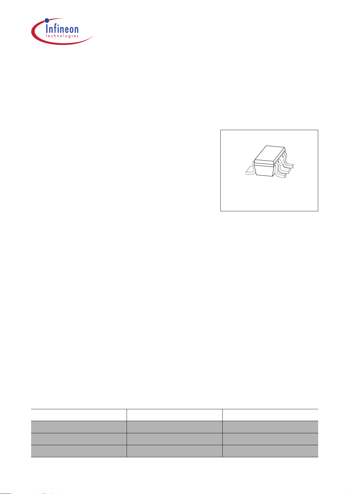
• Very small SMD-Package P-SCT595-5
≤ ±4%
°C ≤ T
≤ 150 °C
j
TLE 4296
SCT 595
Functional Description
The TLE 4296 G is a monolithic integrated low drop voltage regulator in the very small
SMD package P-SCT595-5. It is designed to supply e.g. microprocessor systems under
the severe conditions of automotive applications. Therefore the device is equipped with
additional protection functions against overload, short circuit and reverse polarity. At
overtemperature the regulator is automatically turned off by the integrated thermal
protection circuit.
Input voltages up to 40 V are regulated to
V
Q,nom
= 3.0 V (V30 version) 3.3 V (V33
version) or 5.0 V (V50 version). The output is able to drive a load of more than 30 mA
while it regulates the output voltage within a 4% accuracy.
To save energy the device can be switched in stand-by mode via an inhibit input which
causes the current consumption to drop below 5
µA.
Type Ordering Code Package
TLE 4296 GV30 Q67006-A9339 P-SCT595-5
TLE 4296 GV33 Q67006-A9340 P-SCT595-5
TLE 4296 GV50 Q67006-A9372 P-SCT595-5
Data Sheet 1 Rev. 1.0, 2004-01-01
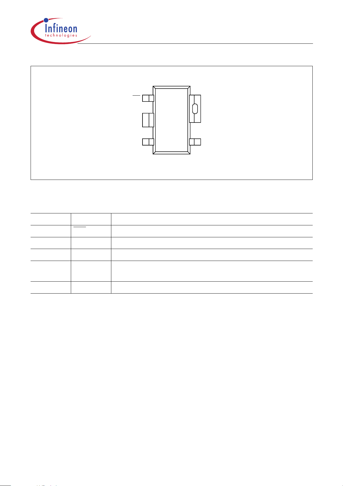
TLE 4296
INH
GND
Ι
1
5
2
3
4
GND
Q
AEP02253
Figure 1 Pin Configuration (top view)
Table 1 Pin Definitions and Functions
Pin No. Symbol Function
1INH
Inhibit input; high level to turn IC on
2GNDGround; connected to pin 5
3IInput voltage
4QOutput voltage; must be blocked by a capacitor
C
≥ 2.2 µF, 3 Ω ≤ ESR ≤ 10 Ω
Q
5GNDGround; connected to pin 2
Data Sheet 2 Rev. 1.0, 2004-01-01
TLE 4296
Temperature
Control
3
Ι
Band-Gap-
Referenz
1
INH
Figure 2 Block Diagram
Saturation
Control and
Protection
Circuit
4
Q
+
2,5
GND
AEB02312
Data Sheet 3 Rev. 1.0, 2004-01-01
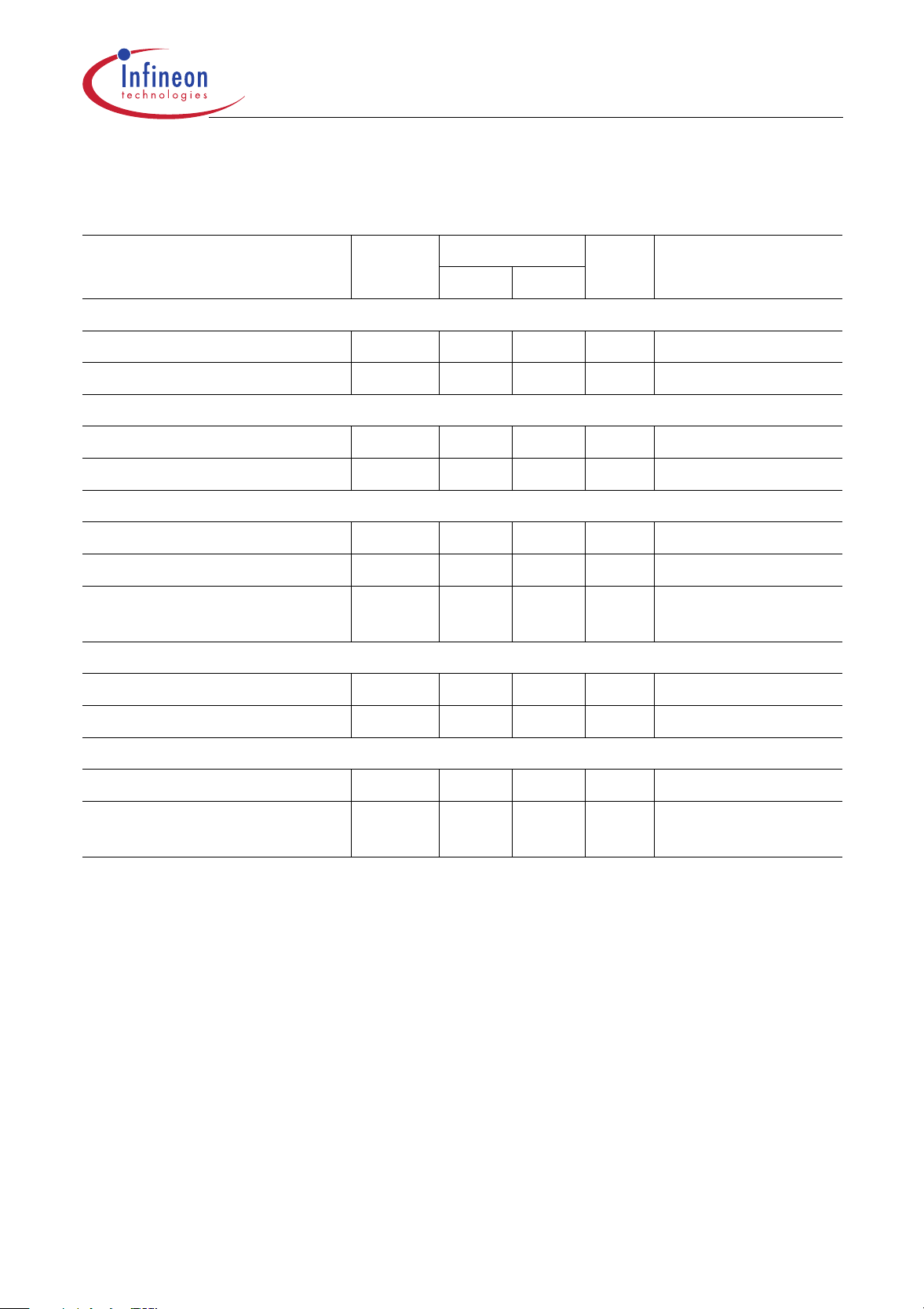
Table 2 Absolute Maximum Ratings
TLE 4296
-40
°C < T
< 150 °C
j
Parameter Symbol Limit Values Unit Remarks
Min. Max.
Input
Voltage
Current
V
I
I
I
-42 45 V –
––mA internally limited
Output
Voltage
Current
V
I
Q
Q
-6 30 V –
––mA internally limited
Inhibit
Voltage
Current
Current
V
I
I
INH
INH
INH
-42 45 V –
-500 * µA * internally limited
-5 5 mA -0.3 V < VI < 45 V;
t
< 1 ms
p
Temperatures
Junction temperature
Storage temperature
T
j
T
stg
-40 150 °C –
-50 150 °C –
Thermal Resistances
Junction pin
Junction ambient
R
thj-pin
1)
R
thja
– 30 K/W measured to pin 5
– 179 K/W zero airflow
zero heat sink area
1) Worst case regarding peak temperature.
Note: Maximum ratings are absolute ratings; exceeding any one of these values may
cause irreversible damage to the integrated circuit.
Data Sheet 4 Rev. 1.0, 2004-01-01

TLE 4296
Table 3 Operating Range
Parameter Symbol Limit Values Unit Remarks
Min. Max.
Input voltage
Inhibit voltage
Junction temperature
V
V
V
V
T
I
I
I
INH
j
4.0 45 V TLE 4296 GV30
4.0 45 V TLE 4296 GV33
5.5 45 V TLE 4296 GV50
-0.3 40 V –
-40 150 °C –
Data Sheet 5 Rev. 1.0, 2004-01-01

TLE 4296
Table 4 Electrical Characteristics
V
= 13.5 V; V
I
Parameter Symbol Limit Values Unit Test Condition
> +2.5 V; -40 °C < Tj < 150 °C; unless otherwise specified
INH
Min. Typ. Max.
Output voltage
V
V30 version
Output voltage
V
V30 version
Output voltage
V
V33 version
Output voltage
V
V33 version
Output voltage
V
V50 version
Output voltage
V
V50 version
Output current limitation
I
Drop voltage V
Output capacitor C
Q
Q
Q
Q
Q
Q
Q
dr
Q
2.88 3.0 3.12 V 1 mA < IQ < 30 mA
V
= 13.5 V
I
2.88 3.0 3.12 V IQ = 10 mA
V
4 V <
< 40 V
I
3.17 3.30 3.43 V 1 mA < IQ < 30 mA
V
= 13.5 V
I
3.17 3.30 3.43 V IQ = 10 mA
4.3 V <
V
< 40 V
I
4.80 5.00 5.20 V 1 mA < IQ < 30 mA
V
= 13.5 V
I
4.80 5.00 5.20 V IQ = 10 mA
6 V <
30 ––mA
1)
– 0.25 0.30 V IQ = 20 mA
V
< 40 V
I
1)
2.2 ––µF3 Ω ≤ ESR ≤ 10 Ω
at 100 kHz
Current consumption
I
= II - I
q
Q
Current consumption
I
= II - I
q
Q
Quiescent current
(stand-by)
I
= II - I
q
Q
Quiescent current
(stand-by)
I
= II - I
q
Q
Load regulation
Line regulation
I
q
I
q
I
q
I
q
∆V
∆V
– 24.5mAIQ < 30 mA
– 110 170 µA IQ < 1 mA;
T
< 85 °C
j
– 01µA V
– 05µA V
Q
Q
– 10 20 mV 1 mA < I
– 5 20mVVI = (V
= 0.4 V;
INH
T
< 85 °C
j
= 0.4 V
INH
T
= 25 °C
j
< 25 mA;
Q
+ 0.5 V)
Q,nom
to 36 V
I
= 5 mA; Tj = 25 °C
Q
Data Sheet 6 Rev. 1.0, 2004-01-01

TLE 4296
Table 4 Electrical Characteristics (cont’d)
V
= 13.5 V; V
I
Parameter Symbol Limit Values Unit Test Condition
> +2.5 V; -40 °C < Tj < 150 °C; unless otherwise specified
INH
Min. Typ. Max.
Power-Supply-RippleRejection
PSRR – 60 – dB f
= 100 Hz;
r
V
Logic Inhibit Input
Inhibit, Turn-on voltage
Inhibit, Turn-off voltage V
H-input current
L-input current
1) Measured when the output voltage VQ has dropped 100 mV from the nominal value.
V
INH, high
INH, low
I
INH, high
I
INH, low
––2.2 V VQ > 0.95 V
0.4 ––V VQ > 0.1 V
– 812µA V
-2 – 2 µA V
= 0.5 Vpp
r
= 5 V
INH
= 0 V
INH
Q,nom
Data Sheet 7 Rev. 1.0, 2004-01-01

Typical Performance Characteristics
V
V
I
versus
Q
AED03348.VSD
V
= 5 V
INH
R
= 1 kΩ
L
Output Voltage
Input Voltage
10
V
V
Q
8
TLE 4296
Current Consumption Iq versus
Input Voltage
1000
µA
I
q
800
V
I
AED03347.VSD
V
= 5 V
INH
6
GV50
4
2
0
0
246810
GV33
GV30
V
V
I
600
400
200
R
= 1 kΩ
L
R
= 5 kΩ
L
0
0
10 20 30 40 50
V
V
I
Data Sheet 8 Rev. 1.0, 2004-01-01

TLE 4296
V
+ 0.5 V to 45 V
Q
,nom
Ι
3
Q
4
3.0V / 3.3V / 5.0V
Inhibit
C
Ι
100 nF
INH
1
TLE 4296 G
2,5
GND
C
Q
2.2 µF
R
Q
Ω
3.3
AES02313
Figure 3 Application Circuit
Application Information
In the TLE 4296 G the output voltage is divided and compared to an internal reference
of 2.5 V typical. The regulation loop controls the output to achieve a stabilized output
voltage.
Figure 3 shows a typical application circuit. In order to maintain the stability of the control
loop the TLE 4296 G output requires an output capacitor
ESR of max. 10
µF / 16V B45196P3335M209 or 4.7 µF / 10 V B45196-P2475M109) or a multi layer
3.3
Ω and min. 3 Ω. It is recommended to use tantalum (e.g. the EPCOS
C
of at least 2.2 µF with an
Q
ceramic capacitor with a series resistor in order to cover these limits over the full
operating temperature range of -40
°C to 150 °C.
At the input of the regulator an input capacitor is necessary for compensating line
influences (100 nF ceramic capacitor recommended). A resistor of approx. 1
C
with
, can damp any oscillation occurring due the input inductivity and the input
I
Ω in series
capacitor.
Data Sheet 9 Rev. 1.0, 2004-01-01

Package Outlines
(0.13)
B
1.2
(0.4)
1)
(0.23)
0.6
+0.1
-0.05
1)
+0.1
-0.05
2.9
(2.2)
±0.2
(0.3)
0.3
0.95
+0.2
acc. to
DIN 6784
+0.1
-0.05
0.25 min
2.6 max
0.20
1.1 max
10˚max
M
A
0.1 max
+0.1
0.15
-0.06
TLE 4296
±0.1
1.6
10˚max
A
1.9
0.25MB
1)
Contour of slot depends on profile
of gull-wing lead form
Figure 4 P-SCT595-5 (Plastic Small Outline)
GPW05997
You can find all of our packages, sorts of packing and others in our
Infineon Internet Page “Products”: http://www.infineon.com/products.
SMD = Surface Mounted Device
Dimensions in mm
Data Sheet 10 Rev. 1.0, 2004-01-01

Edition 2004-01-01
Published by Infineon Technologies AG,
St.-Martin-Strasse 53,
81669 München, Germany
© Infineon Technologies AG 2004.
All Rights Reserved.
Attention please!
The information herein is given to describe certain components and shall not be considered as a guarantee of
characteristics.
Terms of delivery and rights to technical change reserved.
We hereby disclaim any and all warranties, including but not limited to warranties of non-infringement, regarding
circuits, descriptions and charts stated herein.
Information
For further information on technology, delivery terms and conditions and prices please contact your nearest
Infineon Technologies Office (www.infineon.com).
Warnings
Due to technical requirements components may contain dangerous substances. For information on the types in
question please contact your nearest Infineon Technologies Office.
Infineon Technologies Components may only be used in life-support devices or systems with the express written
approval of Infineon Technologies, if a failure of such components can reasonably be expected to cause the failure
of that life-support device or system, or to affect the safety or effectiveness of that device or system. Life support
devices or systems are intended to be implanted in the human body, or to support and/or maintain and sustain
and/or protect human life. If they fail, it is reasonable to assume that the health of the user or other persons may
be endangered.
 Loading...