


现货库存、技术资料、百科信息、热点资讯,精彩尽在鼎好!
TLE4209G
Data Sheet, Rev. 1.3, February 2008
Automotive Power

TLE4209G
Table of Contents
Table of Contents
1 Overview . . . . . . . . . . . . . . . . . . . . . . . . . . . . . . . . . . . . . . . . . . . . . . . . . . . . . . . . . . . . . . . . . . . . . . . 3
2 Block Diagram . . . . . . . . . . . . . . . . . . . . . . . . . . . . . . . . . . . . . . . . . . . . . . . . . . . . . . . . . . . . . . . . . . . 4
3 Pin Configuration . . . . . . . . . . . . . . . . . . . . . . . . . . . . . . . . . . . . . . . . . . . . . . . . . . . . . . . . . . . . . . . . 5
3.1 Pin Assignment . . . . . . . . . . . . . . . . . . . . . . . . . . . . . . . . . . . . . . . . . . . . . . . . . . . . . . . . . . . . . . . . . . . 5
3.2 Pin Definitions and Functions . . . . . . . . . . . . . . . . . . . . . . . . . . . . . . . . . . . . . . . . . . . . . . . . . . . . . . . . 5
4 General Product Characteristics . . . . . . . . . . . . . . . . . . . . . . . . . . . . . . . . . . . . . . . . . . . . . . . . . . . . 6
4.1 Absolute Maximum Ratings . . . . . . . . . . . . . . . . . . . . . . . . . . . . . . . . . . . . . . . . . . . . . . . . . . . . . . . . . 6
4.2 Operating Range . . . . . . . . . . . . . . . . . . . . . . . . . . . . . . . . . . . . . . . . . . . . . . . . . . . . . . . . . . . . . . . . . 6
4.3 Thermal Resistance . . . . . . . . . . . . . . . . . . . . . . . . . . . . . . . . . . . . . . . . . . . . . . . . . . . . . . . . . . . . . . . 7
4.4 Electrical Characteristics . . . . . . . . . . . . . . . . . . . . . . . . . . . . . . . . . . . . . . . . . . . . . . . . . . . . . . . . . . . 7
5 Application Information . . . . . . . . . . . . . . . . . . . . . . . . . . . . . . . . . . . . . . . . . . . . . . . . . . . . . . . . . . 10
6 Package Outlines . . . . . . . . . . . . . . . . . . . . . . . . . . . . . . . . . . . . . . . . . . . . . . . . . . . . . . . . . . . . . . . 13
7 Revision History . . . . . . . . . . . . . . . . . . . . . . . . . . . . . . . . . . . . . . . . . . . . . . . . . . . . . . . . . . . . . . . . 14
Data Sheet 2 Rev. 1.3, 2008-02-04
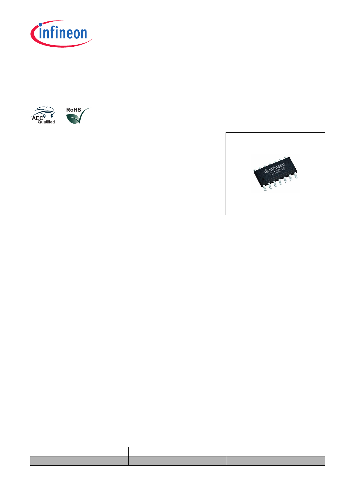
0.8A DC Motor Driver for Servo Driver Applications
1Overview
Features
• Optimized for manual headlight beam control applications
• Delivers up to 0.7 A continuous
• Low saturation voltage; typ.1.6 V total @ 25 °C; 0.7 A
• Output protected against short circuit
• Over temperature protection with hysteresis
• Over- and under voltage lockout
• Internal clamp diodes
• Enhanced SMD power package
• Green Product (RoHS compliant)
• AEC Qualified
TLE4209G
PG-DSO-14-22
Description
The TLE4209G is a protected H-Bridge Driver designed specifically for automotive manual headlight beam control
and industrial servo control applications with DC-brush motor loads.
The part is built using the bipolar high voltage power technology DOPL.
The standard enhanced power PG-DSO-14-22 package meets the application requirements and saves PCBboard space and costs. The package is lead- and halogen-free.
The servo-loop-parameter pos.- and neg. Hysteresis, pos.- and neg. deadband and angle-amplification are
programmable with external resistors.
An internal window-comparator controls the input line. In the case of a fault condition, like short circuit to GND,
short circuit to supply-voltage, and broken wire, the TLE4209G stops the motor immediately (brake condition).
Furthermore the built in features like over- and under voltage-lockout, short-circuit-protection and overtemperature-protection will open a wide range of automotive- and industrial applications.
Type Package Marking
TLE4209G PG-DSO-14-22 TLE4209G
Data Sheet 3 Rev. 1.3, 2008-02-04
TLE4209G
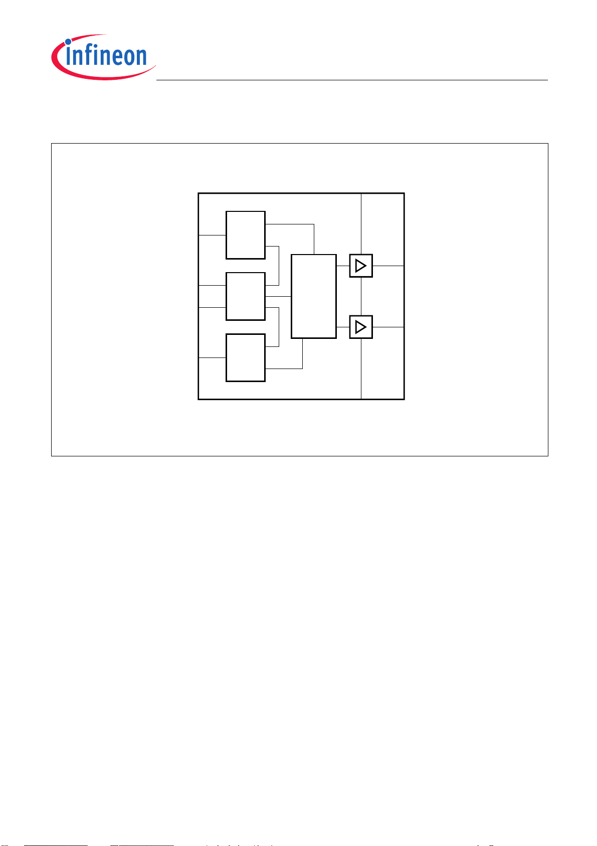
2 Block Diagram
RANGE
REF
FB
HYST
13
14
1
2
Range-
AMP
Servo-
AMP
Hyst-
AMP
TLE 4209G
Protection
and Logic
V
S
8
HalfBridge
HalfBridge
6
OUT1
9
OUT2
Block Diagram
Figure 1 Block Diagram
7
NC
3,4,5,
10,11,12
GND
AEB02258_4209G
Data Sheet 4 Rev. 1.3, 2008-02-04
TLE4209G
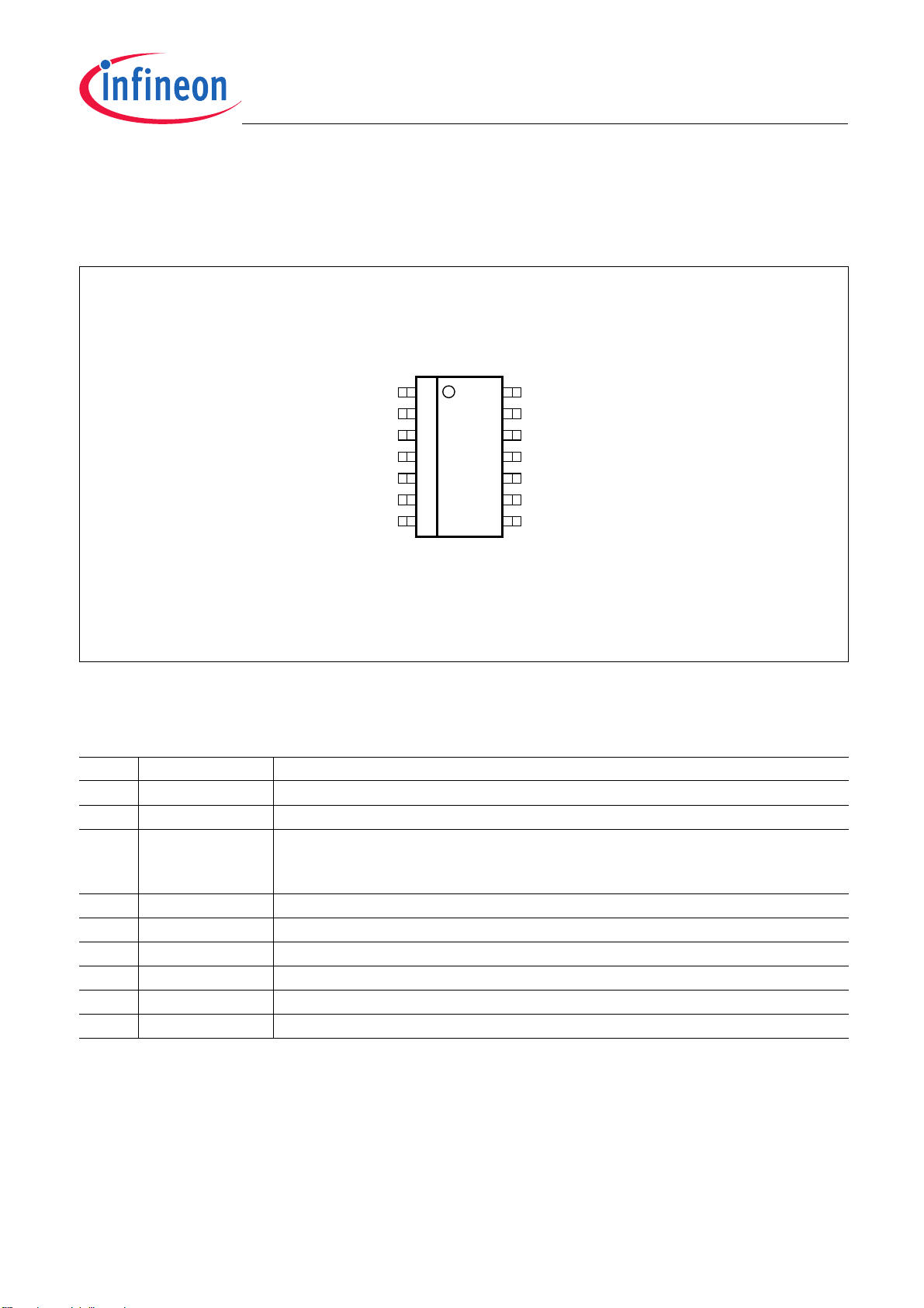
3 Pin Configuration
3.1 Pin Assignment
FB
HYST
GND
GND
GND
OUT1
NC
1
2
3
4
5
6
7
14
13
12
11
10
AEP02261_4209G
9
8
REF
RANGE
GND
GND
GND
OUT2
V
S
Pin Configuration
Figure 2 Pin Configuration
3.2 Pin Definitions and Functions
Pin Symbol Function
1FB Feedback Input
2 HYST Hysteresis I/O
3, 4, 5,
10, 11,
12
6OUT1 Power Output 1
7NC Not Connected
8
9OUT2 Power Output 2
13 RANGE Range Input
14 REF Reference Input
GND Ground
V
S
Power Supply Voltage
Data Sheet 5 Rev. 1.3, 2008-02-04
TLE4209G
General Product Characteristics
4 General Product Characteristics
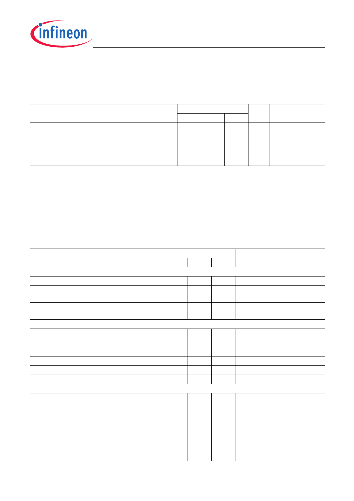
4.1 Absolute Maximum Ratings
Absolute Maximum Ratings
T
= -40 °C to +150 °C; all voltages with respect to ground, positive current flowing into pin
j
(unless otherwise specified)
Pos. Parameter Symbol Limit Values Unit Conditions
Voltages
4.1.1 Supply voltage
4.1.2 Supply voltage
4.1.3 Logic input voltages
(FB, REF, RANGE, HYST)
Currents
4.1.4 Output current (OUT1, OUT2)
4.1.5 Output current (Diode)
4.1.6 Input current
(FB, REF, RANGE, HYST)
Temperatures
4.1.7 Junction temperature
4.1.8 Storage temperature
1) Not subject to production test, specified by design.
1)
Min. Max.
V
V
V
I
I
I
S
S
I
OUT
OUT
IN
-0.3 45 V –
-1 – V t < 0.5 s;
I
> -2 A
S
-0.3 20 V –
– – A internally limited
-0.9 0.9 A –
-2
-6
2
6
mA
mA
t < 2 ms; t/T < 0.1
T
j
T
stg
-40 150 °C–
-50 150 °C–
Note: Stresses above the ones listed here may cause permanent damage to the device. Exposure to absolute
maximum rating conditions for extended periods may affect device reliability.
Note: Integrated protection functions are designed to prevent IC destruction under fault conditions described in the
data sheet. Fault conditions are considered as “outside” normal operating range. Protection functions are
not designed for continuous repetitive operation.
4.2 Operating Range
Pos. Parameter Symbol Limit Values Unit Conditions
Min. Max.
4.2.1 Supply voltage
4.2.2 Supply voltage increasing V
4.2.3 Supply voltage decreasing
4.2.4 Output current
4.2.5 Input current (FB, REF)
4.2.6 Junction temperature
Note: Within the functional range the IC operates as described in the circuit description. The electrical
characteristics are specified within the conditions given in the related electrical characteristics table.
V
S
S
V
S
I
OUT1-2
I
IN
T
j
818VAfter VS rising
-0.3 V
-0.3 V
UV ON
UV OFF
above
V Outputs in tristate
V Outputs in tristate
V
UV ON
-0.7 0.7 A –
-50 500 µA–
-40 150 °C–
Data Sheet 6 Rev. 1.3, 2008-02-04
TLE4209G
General Product Characteristics
4.3 Thermal Resistance
Note: This thermal data was generated in accordance with JEDEC JESD51 standards. For more information, go
to www.jedec.org.
Pos. Parameter Symbol Limit Values Unit Conditions
Min. Typ. Max.
4.3.1 Junction to Soldeering Point
4.3.2 Junction to Ambient
1)
1)
R
R
thJSP
thJA
– – 25 K/W measured to pin 5
– 130 – K/W
2)
minimal-footprint
4.3.3 Junction to Ambient
1)
R
thJA
–65–K/W
3)
additional 600 mm2 CU area
1) Not subject to production test, specified by design.
2) JESD 51-2, 51-3, FR4 76.2 mm × 114.3 mm × 1.5 mm, 70 µm Cu, minimal footprint
3) JESD 51-2, 51-3, FR4 76.2 mm × 114.3 mm × 1.5 mm, 70 µm Cu, 600 mm2 CU cooling area connected to Pins: 3, 4, 5,
10, 11, 12
4.4 Electrical Characteristics
Electrical Characteristics
V
= 8 V to 18 V, Tj = -40 °C to +150 °C, I
S
= 0 A, all voltages with respect to ground, positive current flowing
OUT1-2
into pin (unless otherwise specified)
Pos. Parameter Symbol Limit Values Unit Conditions
Min. Typ. Max.
Current Consumption
4.4.1 Supply current
4.4.2 Supply current
4.4.3 Supply current
I
S
I
S
I
S
– 1220mA–
– 2030mAI
– 3050mAI
OUT1
I
OUT2
OUT1
I
OUT2
= 0.3 A
= -0.3 A
= 0.7 A
= -0.7 A
Over- and Under Voltage Lockout
4.4.4 UV Switch ON voltage
4.4.5 UV Switch OFF voltage
4.4.6 UV ON/OFF Hysteresis
4.4.7 OV Switch OFF voltage V
4.4.8 OV Switch ON voltage
4.4.9 OV ON/OFF Hysteresis
V
UV ON
V
UV OFF
V
UVHY
OV OFF
V
OV ON
V
OVHY
–7.48VVS increasing
6.3 6.9 – V VS decreasing
–0.5–VV
UV ON
- V
UV OFF
– 20.5 23 V VS increasing
17.5 20 – V VS decreasing
–0.5–VV
OV OFF
- V
Outputs OUT1-2, Saturation Voltages
4.4.10 Source (upper)
I
= -0.3 A
OUT
4.4.11 Sink (upper)
I
= -0.7 A
OUT
4.4.12 Sink (lower)
I
= 0.3 A
OUT
4.4.13 Sink (lower)
I
= 0.7 A
OUT
V
V
V
V
SAT U
SAT U
SAT L
SAT L
– 0.901.20V Tj = 25 °C
– 1.101.50V Tj = 25 °C
– 0.250.40V Tj = 25 °C
– 0.450.75V Tj = 25 °C
OV ON
Data Sheet 7 Rev. 1.3, 2008-02-04

TLE4209G
General Product Characteristics
Electrical Characteristics (cont’d)
V
= 8 V to 18 V, Tj = -40 °C to +150 °C, I
S
= 0 A, all voltages with respect to ground, positive current flowing
OUT1-2
into pin (unless otherwise specified)
Pos. Parameter Symbol Limit Values Unit Conditions
Min. Typ. Max.
4.4.14 Total drop
I
= 0.3 A
OUT
4.4.15 Total drop
I
= 0.7 A
OUT
V
SAT
V
SAT
–1.21.7VV
–1.62.5VV
SAT
SAT
= V
= V
SAT U
SAT U
Outputs OUT1-2, Clamp Diodes
4.4.16 Forward voltage; upper
4.4.17 Upper leakage current
4.4.18 Forward voltage; lower
V
I
V
FU
LKU
FL
–11.5VIF = 0.3 A
––5mAIF = 0.3 A
–0.91.4VIF = 0.3 A
Input-Interface, Input REF
4.4.19 Quiescent voltage
4.4.20 Input resistance
V
R
REFq
REF
– 200 – mV I
REF
= 0 µA
–6–kΩ 0 V < V
REF
Input-Interface, Input FB
4.4.21 Quiescent voltage
4.4.22 Input resistance
V
FBq
R
FB
– 200 – mV IFB = 0 µA
–6–kΩ 0 V < VFB < 0.5 V
Input-Interface, Input/Output HYST
4.4.23 Current Amplification
A
HYST
= I
HYST
/ (I
REF
- IFB)
4.4.24 Current Offset
4.4.25 Threshold voltage High
4.4.26 Deadband voltage High
4.4.27 Deadband voltage Low
4.4.28 Threshold voltage Low
4.4.29 Hysteresis Window
4.4.30 Deadband Window V
A
HYST
I
HYSTIO
V
HYH
V
DBH
V
DBL
V
HYL
V
HYW
DBW
0.8 0.95 1.1 – -20 µA < I
-2 0.35 3 µA I
/ VS–52–%–
/ VS– 50.4 – % –
/ VS– 49.6 – % –
/ VS–48–%–
/ VS345%(V
/ VS0.40.81.2% (V
10 µA <
I
REF
V
HYST
REF
V
HYST
I
HYST
= 250 µA;
= VS / 2
= IFB = 250 µA;
= VS / 2
- V
HYH
HYL
- V
DBH
DBL
Input-Interface, Input RANGE
4.4.31 Input current
4.4.32 Switch-OFF voltage High V
4.4.33 Switch-OFF voltage Low V
I
RANGE
OFFH
OFFL
-1 – 1 µA0 V < V
-25 0 100 mV refer to V
RANGE
S
300 400 500 mV refer to GND
+ V
+ V
< 0.5 V
< -10 µA;
HYST
< 20 µA;
) / V
) / V
< V
SAT L
SAT L
S
S
S
Data Sheet 8 Rev. 1.3, 2008-02-04

TLE4209G
Electrical Characteristics (cont’d)
V
= 8 V to 18 V, Tj = -40 °C to +150 °C, I
S
into pin (unless otherwise specified)
Pos. Parameter Symbol Limit Values Unit Conditions
Thermal Shutdown
4.4.34 Thermal shutdown junction
temperature
4.4.35 Thermal switch-on junction
temperature
4.4.36 Temperature hysteresis ∆
1) Not subject to production test, specified by design.
1)
1)
= 0 A, all voltages with respect to ground, positive current flowing
OUT1-2
Min. Typ. Max.
T
jSD
T
jSO
150 175 200 °C–
120 – 170 °C–
T –30–K–
General Product Characteristics
Data Sheet 9 Rev. 1.3, 2008-02-04

TLE4209G
5 Application Information
V
+
R
REF
1 kΩ
B
V
+
V
REFIN
B
R
HYH
100 kΩ
R
R
RANGE
Ω50 k
R
REF
50 k
FB
Ω
R
REF 14
FB 1
50 kΩ
13
Range-
AMP
Servo-
AMP
1N4001
TLE 4209G
Protection
and Logic
Dr
Application Information
C
S
22 µF
Dz
36 V
V
S
8
HalfBridge
OUT1
6
P
Half-
M
Bridge
OUT2
9
FB
1 kΩ
HYST 2
HystAMP
R
HYL
100 k
Ω
GND
Figure 3 Application Diagram
Note: In the application the PIN 7 can remain not connected.
7
NC
3,4,5,
10,11,12
GND
AES02259_4209G
Data Sheet 10 Rev. 1.3, 2008-02-04

TLE4209G
V
V=
V
OUT1
-
OUT2
2.0%0.4%
V( V-)/V
FBREF
Motor
-2.0% -0.4%
Application Information
Motor
Status
Turn
CW
S
Brake
Turn
CCW
DBW
DBL DBH
HYW
HYL HYH
Expressions:
= Hysteresis
HY
DeadbandDB =
HighH=
LowL=
WindowW=
Figure 4 Hysteresis, Phaselag and Deadband-Definitions
AED02260
Data Sheet 11 Rev. 1.3, 2008-02-04

TLE4209G
Tes tconditons:
V
OFFH
V
HYH
V
DBH
V
DBL
V
HYL
V
S
V
FB
V
=
V
; no reverse polarity voltage di ode
S
B
R
=
R
R
HYL
= 50 k
FB
V
REF
= 100 k
HYH
R
=
REF
(t)
(t)
Ω
Ω
(t)
Application Information
V
OFFL
S ta r t-C omman d
Stop-Command
V
OUT2
H
L
V
OUT1
H
L
B = Brake
t
t
BBCWBCWBBMotor Status
CCW
CCW
t
Figure 5 Timing and Phaselag
Data Sheet 12 Rev. 1.3, 2008-02-04

TLE4209G
6 Package Outlines
1.27
+0.1
0.41
-0.06
14
0.1 MIN.
M
0.28A
(1.5)
0.1
C
14x
4
1.75 MAX.
C
-0.2
0.33
1)
6
±0.08
±0.2
x 45˚
0.64
+0.05
-0.01
0.2
Package Outlines
MAX.8˚
±0.25
1
8.75
Index Marking
1)
Does not include plastic or metal protrusion of 0.15 max. per side
-0.2
7
1)
A
GPS09033
Figure 6 PG-DSO-14-22 (Plastic Green - Dual Small Outline Package)
Green Product (RoHS compliant)
To meet the world-wide customer requirements for environmentally friendly products and to be compliant with
government regulations the device is available as a green product. Green products are RoHS-Compliant (i.e
Pb-free finish on leads and suitable for Pb-free soldering according to IPC/JEDEC J-STD-020).
You can find all of our packages, sorts of packing and others in our
Infineon Internet Page “Products”: http://www.infineon.com/products.
Dimensions in mm
Data Sheet 13 Rev. 1.3, 2008-02-04

TLE4209G
7 Revision History
Revision Date Changes
1.1
1.2
1.3
2007-04-11
2007-08-10
2008-02-04
RoHS-compliant DSO package version of the TLE 4209
All pages: Infineon logo updated
Page 1:
“AEC qualified” and “RoHS” logo added, “Green Product (RoHS compliant)” and
“AEC qualified” statement added to feature list, package names changed to
RoHS compliant versions, package pictures updated
Page 13:
Package names changed to RoHS compliant versions, “Green Product”
description added
Revision History added
Legal Disclaimer added
Package name changed to PG-DSO-14-22
Page 1: Editorial change: deleted "fully" (The term "fully protected" often leads to
misunderstandings as it is unclear with respect to which parameters).
Revision History
Data Sheet 14 Rev. 1.3, 2008-02-04

Edition 2008-02-04
Published by
Infineon Technologies AG
81726 Munich, Germany
© 2008 Infineon Technologies AG
All Rights Reserved.
Legal Disclaimer
The information given in this document shall in no event be regarded as a guarantee of conditions or
characteristics. With respect to any examples or hints given herein, any typical values stated herein and/or any
information regarding the application of the device, Infineon Technologies hereby disclaims any and all warranties
and liabilities of any kind, including without limitation, warranties of non-infringement of intellectual property rights
of any third party.
Information
For further information on technology, delivery terms and conditions and prices, please contact the nearest
Infineon Technologies Office (www.infineon.com).
Warnings
Due to technical requirements, components may contain dangerous substances. For information on the types in
question, please contact the nearest Infineon Technologies Office.
Infineon Technologies components may be used in life-support devices or systems only with the express written
approval of Infineon Technologies, if a failure of such components can reasonably be expected to cause the failure
of that life-support device or system or to affect the safety or effectiveness of that device or system. Life support
devices or systems are intended to be implanted in the human body or to support and/or maintain and sustain
and/or protect human life. If they fail, it is reasonable to assume that the health of the user or other persons may
be endangered.
 Loading...