

现货库存、技术资料、百科信息、热点资讯,精彩尽在鼎好!
1-A Dual-HBD (Dual-Half-Bridge Driver) TLE4207G
Features
• Delivers up to 0.8 A continuous
• Optimized for DC motor management applications
• Very low current consumption
in stand-by (Inhibit) mode
• Low saturation voltage
0.4 A
• Output protected against short circuit
• Error flag diagnosis
• Overvoltage lockout and diagnosis
• Undervoltage lockout
• CMOS/TTL compatible inputs with hysteresis
• No crossover current
• Internal clamp diodes
• Overtemperature protection with hysteresis
and diagnosis
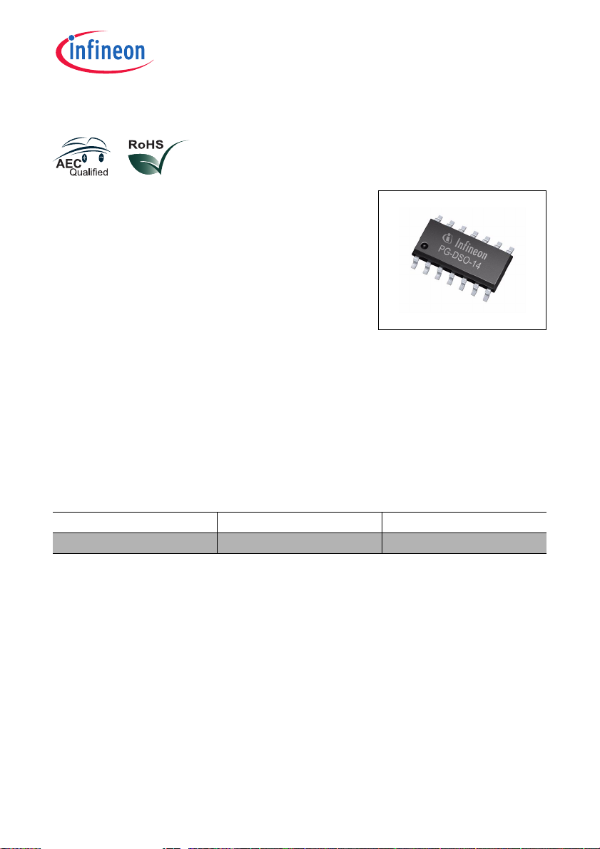
• Enhanced power PG-DSO-Package
• Green Product (RoHS compliant)
• AEC Qualified
Type Ordering Code Package
TLE4207G on request PG-DSO-14-22
; typ.1.2 V total @ 25 °C;
PG-DSO-14-22
Description
The TLE4207G is a protected Dual-Half-Bridge-Driver designed specially for automotive
and industrial motion control applications.
The part is built using the Infineon bipolar high voltage power technology DOPL.
The actuator (DC motor) can be connected direct between the halfbridges. Operation
modes forward (cw), reverse (ccw), brake and high impedance are invoked from a
standard interface. The standard enhanced power PG-DSO-14-22 package meets the
application requirements and saves PCB-board space and costs.
Furthermore the built in features like diagnosis, over- and undervoltage-lockout, shortcircuit-protection, over-temperature-protection and the very low quiescent current in
stand-by mode will open a wide range of automotive and industrial applications.
Data Sheet 1 Rev. 1.1, 2008-01-08
V
1
S
OUT2
GND
GND
GND
IN2
INH
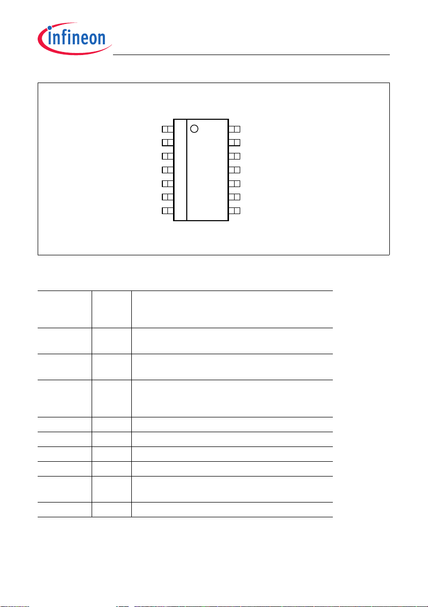
Figure 1 Pin Configuration (top view)
Pin Definitions and Functions
Pin No.
PG-DSO14-22
1
2OUT2Power output 2; short circuit protected;
3, 4, 5,
10, 11, 12
6IN2Input channel 2; controls OUT2 (not inverted)
7INHInhibit input; low = IC in stand-by
8EFError Flag output; open collector; low = error
9IN1Input channel 1; controls OUT1 (not inverted)
13 OUT1 Power output 1; short circuit protected;
14 N.C. Not connected
Symbol Function
V
S
GND Ground;
Power supply voltage;
positive reference potential for blocking capacitor
with integrated clamp diodes
negative reference potential for blocking
capacitor
with integrated clamp diodes
2
3
4
5
6
7
TLE
4207G
AEP02303
14
13
12
11
10
N.C.
OUT1
GND
GND
GND
IN1
9
8
EF
TLE4207G
Data Sheet 2 Rev. 1.1, 2008-01-08
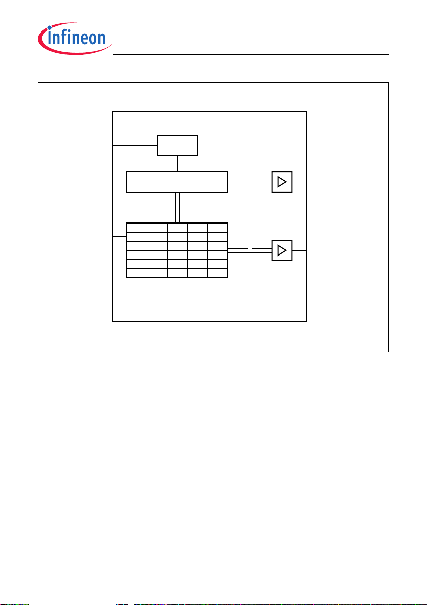
TLE4207G
V
S
1
7
INH
Inhibit
8
EF
9
IN1
IN2
0
1
6
1
1
1
4207GTLE
Figure 2 Block Diagram
Fault-Detection
IN2 OUT2
OUT1IN1INH
XXZZ
00
0
1
0
1
11
LL
HL
LH
HH
DRV1
DRV2
3, 4, 5,
10, 11, 12
GND
13
OUT1
2
OUT2
AEB02080
Data Sheet 3 Rev. 1.1, 2008-01-08

Functional Truth Table
INH IN1 IN2 OUT1 OUT2 Mode
0 X X Z Z Stand-By
1
1
1
1
0
0
1
1
0
1
0
1
L
L
H
H
L
H
L
H
Brake LL
CW
CCW
Brake HH
IN: 0 = Logic LOW OUT: Z = Output in tristate condition
1 = Logic HIGH L = Output in sink condition
X = don’t care H = Output in source condition
Diagnosis
EF Error
1
0
0
no error
over temperature
over voltage
TLE4207G
Data Sheet 4 Rev. 1.1, 2008-01-08
Electrical Characteristics
Absolute Maximum Ratings
Parameter Symbol Limit Values Unit Remarks
min. max.
Voltages
TLE4207G
Supply voltage
Supply voltage
Logic input voltages
V
S
V
S
V
I
– 0.3 45 V –
– 1 – V t < 0.5 s; IS > – 2 A
– 5 20 V 0 V < VS < 45 V
(IN1; IN2; INH)
Logic output voltage (EF)
V
EF
– 0.3 20 V 0 V < VS < 45 V
Currents
Output current (cont.) I
Output current (peak)
Output current (diode)
Output current (EF)
OUT1-2
I
OUT1-2
I
OUT1-2
I
OUT1-2
– – A internally limited
– – A internally limited
–1 1 A –
–2 5 mA –
Temperatures
Junction temperature
Storage temperature
T
j
T
stg
– 40 150 °C–
– 50 150 °C–
Thermal Resistances
Junction pin
Junction ambient
R
R
thj-pin
thjA
– 25 K/W measured to pin 5
–65K/W–
Note: Maximum ratings are absolute ratings; exceeding any one of these values may
cause irreversible damage to the integrated circuit.
Data Sheet 5 Rev. 1.1, 2008-01-08

TLE4207G
Operating Range
Parameter Symbol Limit Values Unit Remarks
min. max.
Supply voltage
Supply voltage increasing
Supply voltage decreasing
Logic input voltage
V
S
V
S
V
S
V
I
(IN1; IN2; INH)
Junction temperature
T
j
Note: In the operating range the functions given in the circuit description are fulfilled.
V
UV OFF
18 V After VS rising
above V
– 0.3 V
– 0.3 V
UV ON
UV OFF
V Outputs in tristate
V Outputs in tristate
– 2 18 V –
– 40 150 °C–
UV ON
Data Sheet 6 Rev. 1.1, 2008-01-08

TLE4207G
Electrical Characteristics
V
8 V <
< 18 V; INH = High; I
S
unless otherwise specified
Parameter Symbol Limit Values Unit Test Condition
Current Consumption
= 0 A; – 40 °C < Tj < 150 °C;
OUT1-2
min. typ. max.
Quiescent current
Quiescent current
Supply current
Supply current
Supply current
I
S
I
S
I
S
I
S
I
S
Over- and Under Voltage Lockout
UV Switch ON voltage
UV Switch OFF voltage
UV ON/OFF hysteresis
OV Switch OFF voltage V
OV Switch ON voltage
OV ON/OFF hysteresis
V
UV ON
V
UV OFF
V
UV HY
OV OFF
V
OV ON
V
OV HY
–2050µA INH = LOW
–2030µA INH = LOW;
V
= 13.2 V;
S
T
= 25 °C
j
–1020mA–
––30mAI
––50mAI
OUT1
I
OUT2
OUT1
I
OUT2
= 0.4 A
= – 0.4 A
= 0.8 A
= – 0.8 A
–6.57.5VVS increasing
5.0 6 – V VS decreasing
–0.5–VV
UV ON
– V
UV OFF
–2024VVS increasing
18.0 19.5 – V VS decreasing
–0.5–VV
OV OFF
– V
OV ON
Data Sheet 7 Rev. 1.1, 2008-01-08

TLE4207G
Electrical Characteristics (cont’d)
V
8 V <
< 18 V; INH = High; I
S
unless otherwise specified
Parameter Symbol Limit Values Unit Test Condition
Outputs OUT1-2
Saturation Voltages
= 0 A; – 40 °C < Tj < 150 °C;
OUT1-2
min. typ. max.
Source (upper)
I
= – 0.2 A
OUT
Source (upper)
I
= – 0.4 A
OUT
Sink (upper)
I
= – 0.8 A
OUT
Sink (lower)
I
= 0.2 A
OUT
Sink (lower)
I
= 0.4 A
OUT
Sink (lower)
I
= 0.8 A
OUT
I
Total Drop
Total Drop I
Total Drop I
= 0.2 A V
OUT
= 0.4 A V
OUT
= 0.8 A V
OUT
Clamp Diodes
Forward voltage; upper
Upper leakage current
Forward voltage; lower V
Notes see page 10.
V
V
V
V
V
V
V
I
LKU
SAT U
SAT U
SAT U
SAT L
SAT L
SAT L
SAT
SAT
SAT
FU
FL
– 0.85 1.15 V Tj = 25 °C
– 0.90 1.20 V Tj = 25 °C
– 1.10 1.50 V Tj = 25 °C
– 0.15 0.23 V Tj = 25 °C
– 0.25 0.40 V Tj = 25 °C
– 0.45 0.75 V Tj = 25 °C
V
–11.4V
–1.21.7V
–1.62.5V
= V
SAT
SAT U
V
= V
SAT
SAT U
V
= V
SAT
SAT U
–11.5VIF = 0.4 A
––5mAIF = 0.4 A
–0.91.4VIF = 0.4 A
+ V
SAT L
+ V
SAT L
+ V
SAT L
1)
Data Sheet 8 Rev. 1.1, 2008-01-08

TLE4207G
Electrical Characteristics (cont’d)
V
8 V <
< 18 V; INH = High; I
S
unless otherwise specified
Parameter Symbol Limit Values Unit Test Condition
Input-Interface
Logic Inputs IN1; IN2
= 0 A; – 40 °C < Tj < 150 °C;
OUT1-2
min. typ. max.
H-input voltage
L-input voltage
Hysteresis of input voltage
H-input current
L-input current
Logic Input INH
H-input voltage V
L-input voltage
Hysteresis of input voltage
H-input current
L-input current
Error-Flag EF
L-output voltage level V
Leakage current
V
V
V
I
IH
I
IL
V
V
I
IH
I
IL
I
EFLK
IH
IL
IHY
IH
IL
IHY
EFL
–23V–
11.5–V–
–0.5–V–
–2 – 10 µA VI = 5 V
– 100 – 20 – 5 µA VI = 0 V
–2.73.5V–
12–V–
–0.7–V–
– 100 250 µA V
–10 – 10 µA V
INH
INH
= 5 V
= 0 V
–0.20.4VIEF =2 mA
– –10µA0V < VEF < 7 V
Data Sheet 9 Rev. 1.1, 2008-01-08

TLE4207G
Electrical Characteristics (cont’d)
V
8 V <
< 18 V; INH = High; I
S
unless otherwise specified
Parameter Symbol Limit Values Unit Test Condition
Thermal Shutdown
= 0 A; – 40 °C < Tj < 150 °C;
OUT1-2
min. typ. max.
Thermal shutdown junction
T
jSD
150 175 200 °C–
temperature
Thermal switch-on junction
T
jSO
120 – 170 °C–
temperature
Temperature hysteresis ∆
1) Guaranteed by design.
T –30–K–
Note: The listed characteristics are ensured over the operating range of the integrated
circuit. Typical characteristics specify mean values expected over the production
spread. If not otherwise specified, typical characteristics apply at TA = 25 °C and
the given supply voltage.
Data Sheet 10 Rev. 1.1, 2008-01-08

TLE4207G
Watchdog
WD R
Reset
TLE 4268G
Q
R
Q
10 k Ω
V
CC
INH
C
Q
22 F
7
D GND
C
D
µµ
100nF
Inhibit
I
V
S
DO1
1N4001
V = 12 V
S
C
S
F22
1
EF
8
P
µ
IN1
9
0
IN2
1
6
1
1
1
Figure 3 Application Circuit
Fault-Detection
IN2 OUT2
OUT1IN1INH
XXZZ
00
0
1
0
1
11
4207GTLE
DRV1
OUT1
13
M1
DRV2
OUT2
LL
2
HL
LH
HH
3, 4, 5,
10, 11, 12
GND
AES02081
Data Sheet 11 Rev. 1.1, 2008-01-08

Diagrams
Quiescent current
I
over Temperature
50
Ι
S
µ
A
40
30
20
10
S
VS= 18 V
= 13.2 V
V
S
V
= 8 V
S
AED02307
TLE4207G
Saturation Voltage of Source V
over Temperature
1500
V
SAT U
= 14 V
V
S
1250
mV
1000
750
500
250
Ι
OUT
Ι
OUT
Ι
OUT
= 800 mA
= 400 mA
= 200 mA
SAT U
AED02308
0
-50
0 50 100 150
Saturation Voltage of Sink
over Temperature
1000
V
SAT L
= 14 V
V
S
mV
750
= 800 mA
Ι
500
250
0
-50
OUT
= 400 mA
Ι
OUT
= 200 mA
Ι
OUT
0 50 100 150
V
SAT L
˚C
T
j
AED02309
˚C
T
j
Total Drop at outputs
over Temperature
0
-50
2000
V
SAT
mV
0 50 100 150
V
= 14 V
V
S
= 800 mA
Ι
OUT
SAT
˚C
T
j
AED02310
1500
= 400 mA
Ι
OUT
= 200 mA
Ι
1000
OUT
500
0
-50
0 50 100 150
˚C
T
j
Data Sheet 12 Rev. 1.1, 2008-01-08

Package Outlines
PG-DSO-14-22
(Plastic Green - Dual Small Outline Package)
TLE4207G
Green Product (RoHS compliant)
To meet the world-wide customer requirements for environmentally friendly products
and to be compliant with government regulations the device is available as a green
product. Green products are RoHS-Compliant (i.e Pb-free finish on leads and suitable
for Pb-free soldering according to IPC/JEDEC J-STD-020).
Sorts of Packing
Package outlines for tubes, trays etc. are contained in our
SMD = Surface Mounted Device
Data Sheet 13 Rev. 1.1, 2008-01-08
Dimensions in mm

TLE4207G
Revision History
Version Date Changes
Rev. 1.1 2008-01-08 Initial version of RoHS-compliant derivate of TLE4207G
Page 1: added AEC certified statement
Page 1 and 13: added RoHS compliance statement and
Green product feature
Page 1+2: Editorial change: deleted "fully" (The term "fully
protected" often leads to misunderstandings as it is unclear
with respect to which parameters).
Page 1 and 13: Package changed to RoHS compliant version
Page 14 and 15: added Revision History, updated Legal
Disclaimer
Data Sheet 14 Rev. 1.1, 2008-01-08

Edition 2008-01-08
Published by
Infineon Technologies AG
81726 Munich, Germany
© 2/4/08 Infineon Technologies AG
All Rights Reserved.
Legal Disclaimer
The information given in this document shall in no event be regarded as a guarantee of conditions or
characteristics. With respect to any examples or hints given herein, any typical values stated herein and/or any
information regarding the application of the device, Infineon Technologies hereby disclaims any and all warranties
and liabilities of any kind, including without limitation, warranties of non-infringement of intellectual property rights
of any third party.
Information
For further information on technology, delivery terms and conditions and prices, please contact the nearest
Infineon Technologies Office (www.infineon.com).
Warnings
Due to technical requirements, components may contain dangerous substances. For information on the types in
question, please contact the nearest Infineon Technologies Office.
Infineon Technologies components may be used in life-support devices or systems only with the express written
approval of Infineon Technologies, if a failure of such components can reasonably be expected to cause the failure
of that life-support device or system or to affect the safety or effectiveness of that device or system. Life support
devices or systems are intended to be implanted in the human body or to support and/or maintain and sustain
and/or protect human life. If they fail, it is reasonable to assume that the health of the user or other persons may
be endangered.
 Loading...