

Page 1

UM TLD5542-1 eval
TLD5542-1 Multichannel evalboard V4.5
User Manual
About this document
Product description
TLD5542-1QV: H-Bridge buck-boost DC/DC controller designed for high power, high efficiency automotive
applications
• Constant current (LED) and constant voltage regulation
• SPI for diagnostics and control
• Limp Home function (fail-safe mode)
• EMC optimized device: Spread Spectrum
Scope and purpose
Scope of this user manual is to provide to the audience instructions on usage of the TLD5542-1 Multichannel
evalboard V4.4 and relative PC GUI.
The TLD5542-1 Multichannel evalboard V4.4 it is an evaluation platform for the TLD5542-1, which can drive 3 LED
functions (HB, LB, DRL), with a single efficient DC/DC converter. The board shows good EMC performance, EMC
report available for download on the evaluation board webpage.
Intended audience
Hardware engineers, software engineers, system architects
User Manual Please read the Important Notice and Warnings at the end of this document Rev.1.12
www.infineon.com page 1 of 17 2020-04-02
Page 2

TLD5542-1 Multichannel evalboard V4.5
User Manual
Table of contents
1 Table of contents
About this document ......................................................................................................................... 1
1 Table of contents ...................................................................................................................... 2
2 Glossary .................................................................................................................................. 3
3 Description .............................................................................................................................. 4
4 Quick start procedure ............................................................................................................... 5
5 Possible light scenarios ............................................................................................................. 8
6 Operating range and power derating ......................................................................................... 9
7 Electrical characteristics ..........................................................................................................10
8 Diagnostic ..............................................................................................................................11
9 PCB layout ..............................................................................................................................12
10 Schematic ...............................................................................................................................13
Revision history ...............................................................................................................................16
User Manual 2 of 17 Rev.1.12
2020-04-02
Page 3

TLD5542-1 Multichannel evalboard V4.5
User Manual
2 Glossary
DRL: Daytime Running Light function
POS: position light obtained by dimming down the DRL function
LB: Low Beam function
HB: High Beam function
H-Bridge: 4 switches topology buck-boost DC/DC converter (see Figure 1)
Figure 1 4 switches H-Bridge architecture overview
User Manual 3 of 17 Rev.1.12
2020-04-02
Page 4

TLD5542-1 Multichannel evalboard V4.5
User Manual
3
The TLD5542-1 multichannel evalboard V4.4 it is an evaluation platform for the TLD5542-1, which can drive 3 LED
functions (HB, LB, DRL), with a single efficient DC/DC converter.
In the single DC/DC multichannel system night-time functions (e.g. HB and LB) are connected in series and the
complementary daytime (DRL) function in parallel by mean of switches (Figure 2). The switches properly
distribute the DC/DC converter output current in order to obtain the requested LED currents. This approach is
called multi floating switch (MFS) architecture.
Description
Figure 2 LED driver with 3 functions on MFS architecture
The TLD5542-1 Multichannel evalboard V4.4 has an ePower microcontroller TLE9842-2 pre-programmed with the
application software V4.0 or higher. A PC GUI can configure load currents and duty cycles via USB (UART over
LIN).
Figure 3
TLD5542-1 Multichannel evalboard V4.4
On the board, in addition the following are present:
•
A 300 mA LS switch to drive an external FAN
•
Limp Home push button show fail safe operation
•
Extra push button whose functionality can be programmed by the user
•
LIN interface and a detachable USB serial to LIN daughter board
User Manual 4 of 17 Rev.1.12
2020-04-02
Page 5

TLD5542-1 Multichannel evalboard V4.5
User Manual
4
The TLD5542-1 multichannel evalboard comes with USB to LIN daughter board, avoid detaching it from the
main board in order to be able to control the board via USB.
Humming noise may be heard from the board due to piezoelectric effect on output capacitors, this does not
affect the performance.
Step by step procedure
1.
Connect the load(s) to the HB, LB, DRL connectors as shown in Figure 4 , the software will automatically
disable unconnected terminals
Quick start procedure
Figure 4 TLD5542-1 Multichannel evalboard V4.4 - connect loads
2.
Connect a 12 V 5 A power supply to the VIN connector
Figure 5 TLD5542-1 Multichannel evalboard V4.4 - connect power supply
3.
Load will be powered with Default configuration:
LB 1000 mA, HB 800 mA , POS 28 mA (400 mA @ 7%)
4.
In order to control the TLD5542-1 Multichannel evalboard, install the GUI V1.0 to the control PC (chapter
Error! Reference source not found.)
User Manual 5 of 17 Rev.1.12
2020-04-02
Page 6

TLD5542-1 Multichannel evalboard V4.5
User Manual
5.
Connect a micro USB cable from the TLD5542-1 evalboard to the PC (Figure 6)
Figure 6 Connect a microUSB cable from the PC to the evalBoard
6.
Launch the “TLD5542-1_MULTICH_GUI_V1.0.xlsm” to execute the excel GUI ( Figure 7 )
Figure 7 TLD5542-1 Excel GUI V1.0 screenshot on communication established
7.
Connection cell will turns green (Figure 7) on the GUI if the right COM port is selected
8.
Select desired load current and duty cycle and press “Send Configuration” button
9.
LED load will be powered with selected configuration
Note:
Due to the schematic implementation, if POS is ON, then the maximum possible duty cycle on LB/HB is reduced by
the POS duty cycle + load change time (duty cycle losses: Figure 8). The software automatically increases the
LB/HB current to keep average current equal to the requested current, so peak current could be different than the
requested one. During LB/HB+POS scenario, POS duty cycle has to be < 10% in order to minimize LB/HB current
increase.
User Manual 6 of 17 Rev.1.12
2020-04-02
Page 7

TLD5542-1 Multichannel evalboard V4.5
User Manual
Example: User requested scenario is:
LB current = 1 A @100% duty POS = 300 mA @7% duty
Produced scenario (depending by LB and DRL voltage):
LB current = 1.14 A @88% duty=> 1A avg POS = 300 mA @ 7% duty
Figure 8 Time sharing and duty cycle losses
For further information please read the TLD5542-1 cost optimized application note and SW description documents:
Infineon-Z8F67062262_Cost_Optimized_TLD5542-AN.pdf
Infineon-Z8F64914635_TLD5542-1_Software_Description-AN.pdf
User Manual 7 of 17 Rev.1.12
2020-04-02
Page 8

TLD5542-1 Multichannel evalboard V4.5
User Manual
5 Possible light scenarios
On the TLD5542-1 multichannel evalboard, LB (master) and HB (slave) channels are connected in series, so that
the instantaneous current on the 2 strings is the same. Different average current can be achieved by applying
PWM dimming to the HB.
HB duty cycle can be smaller or equal to the LB duty cycle.
Table 1 TLD5542-1 Multichannel evalboard V4.4 - possible light scenarios
LB HB DRL POS (<10% duty)
LB ON ANY OFF ANY
HB ON ON OFF ANY
DRL OFF OFF ON OFF
POS ANY ANY OFF ON
DEFAULT
ON
(1000 mA)
ON
(800 mA)
OFF
ON
(28 mA = 400 mA@7%)
By pressing Limp Home button on the evalboard, LHI pin of the TLD5542-1 is activated, and the bypass switches
are configured by a dedicated circuitry in order to power LB only @ 850 mA. The μC SPI commands and GPIOs
are ignored, simulating a fail-safe operation. The resistor divider on the SET pin configures the output current
in limp home operation (850 mA).
User Manual 8 of 17 Rev.1.12
2020-04-02
Page 9

TLD5542-1 Multichannel evalboard V4.5
User Manual
6 Operating range and power derating
Software power derating is implemented on SW 3.8, and it reduces output current (and thus the output power)
when the battery voltage drops below 9V at the board connector. Power derating profile is set as shown in
Figure 9 (6W/V).
P
[W]
out
50
40
32
25
P
out-peak
P
out-average
6
9
18
V
[V]
bat
Figure 9 Average (blue) and peak (red) output power derating profile
The SW V3.8 is limits only the peak output power (red curve on Figure 9), but if POS function is ON, then the
effective LB/HB average power available on LB is reduced to Pout-average (blue curve on Figure 9).
Please note that the module does not implement thermal protection, so ensure proper cooling when output
power is above 30 W. Place a heat sink below switching MOSFETs as shown on Figure 10.
Figure 10 TLD5542-1 Heat sink placement
The Heat sink should be thermally coupled but electrically insulated from the PCB by mean of a thermal pad.
User Manual 9 of 17 Rev.1.12
2020-04-02
Page 10

V
V
TLD5542-1 Multichannel evalboard V4.5
User Manual
7 Electrical characteristics
Table 2 TLD5542-1 multichannel evalboard V4.4 – electrical characteristics
Parameter Symbol
Unit Note/Test Condition
Min Typ Max
Value
Input Voltage
Out voltage
Output current
HB,LB average
Output current
DRL
Output Power
Switching
frequency
PWM frequency PWM
VIN (Normal)
VIN (Extended)
VIN (Survival)
3 – 50
OUT
(HB,LB)
I
OUT
(DRL/POS) 250 – 1500 mA
I
OUT
(LB,HB)
P
OUT
(DRL)
P
OUT
Switching
frequency
200 – – Hz –
freq
System efficiency Eff – 93 – %
9
6
-18
250
250
18
–
18
V ˜
+40
–
1350
mA
–
1200
mA
3 – 40 W
– 384 – kHz Spread Spectrum deviation is present
–
scenario = LB/HB only POS = OFF
scenario = LB/HB + POS, POS duty cycle < 10%
CHA and CHB string voltage difference < 30 V
Limited by software power derating
Average Pout for
VIN down to 9V
Board efficiency, including μC:
LB 5 LED 1200 mA,
HB 4 LED 960 mA ,
POS 10 LED 400 mA @7%
= 13.5 V
V
IN
= 34.7 W
P
IN
(LB+HB+DRL)= 32.4 W
P
OUT
User Manual 10 of 17 Rev.1.12
2020-04-02
Page 11

TLD5542-1 Multichannel evalboard V4.5
User Manual
8 Diagnostic
TLD5542-1 multichannel software version 4.0 (or higher) is able to detect several failures on the LED load:
Table 3 Failure detection
Failure type Description
LB (FA2)
Open
Short
FA2 open is always reported as FA2 & FA3 open due to schematic
implementation
When FA2(LB) fails, also FA3(HB) is disabled, DRL/POS is available
HB (FA3) Open/Short When FA3(HB) fails , FA2 (LB) and DRL/POS are still available
DRL/POS Open/ShortT When DRL/POS fails , FA2 (LB) and FA3(HB) are still available
Undervoltage (V
< 6 V)
IN
Restart after V
undervoltage when VIN > 8 V
IN
VIN
Overvoltage (V
> 20 V)
IN
Restart after V
overvoltage when VIN < 18 V
IN
A function is considered shorted if its voltage is below 2 V.
Diagnostic is visible also on the PC GUI as shown on Figure 11.
Figure 11 TLD5542-1 PC GUI: diagnostic indicators
User Manual 11 of 17 Rev.1.12
2020-04-02
Page 12
TLD5542-1 Multichannel evalboard V4.5
User Manual
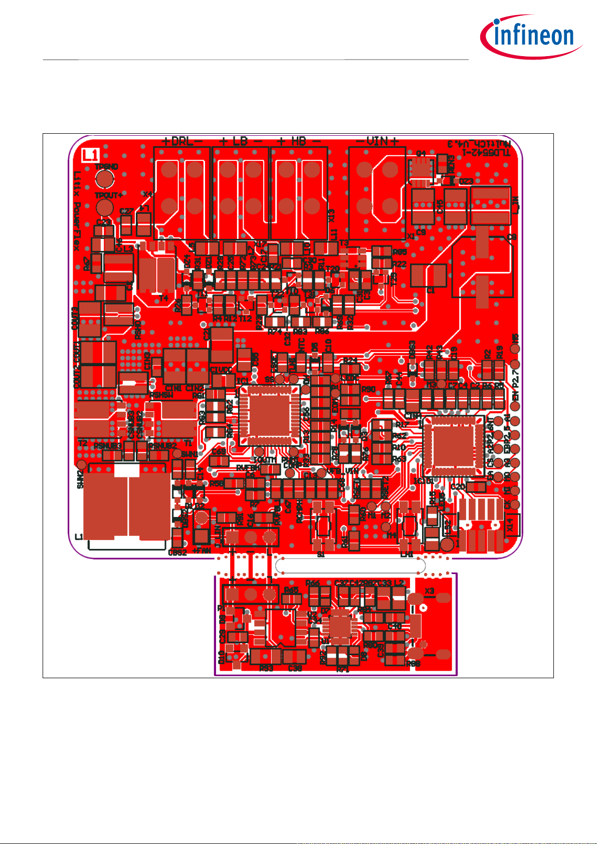
9 PCB layout
Figure 12 PCB layout top view
User Manual 12 of 17 Rev.1.12
2020-04-02
Page 13

TLD5542-1 Multichannel evalboard V4.5
User Manual
10 Schematic
User Manual 13 of 17 Rev.1.12
2020-04-02
Page 14

TLD5542-1 Multichannel evalboard V4.5
User Manual
User Manual 14 of 17 Rev.1.12
2020-04-02
Page 15

TLD5542-1 Multichannel evalboard V4.5
User Manual
User Manual 15 of 17 Rev.1.12
2020-04-02
Page 16

e
e
n
s
n
n
y
n
y
e
n
Revision history
Document
Date of release Description of changes
version
Rev. 1.00 2020-01-14 Initial User Manual
Rev. 1.10 2020-01-16 Updated LED load symbol polarity on Figure 4
Rev. 1.10 2020-01-16 Added USB connection image: Figure 6
Rev. 1.10 2020-01-16 Updated GUI screenshots with SW version
Rev. 1.10 2020-01-16 Updated Labview installation version 2018
Rev. 1.10 2020-01-16 correct Switching frequency to 384 kHz on Electrical characteristics
Rev. 1.11 2020-02-05 Updated SCH to version 4.5
Rev. 1.12 2020-04-02 Updated with excel GUI V1.0
Trademarks
All referenced product or service names and trademarks are the property of their respective owners.
Edition 2020-04-02
Published by
Infineon Technologies AG
81726 München, Germany
© 2020 Infineon Technologies AG.
All Rights Reserved.
Do you have a question about this
document?
Email: erratum@infineon.com
Document reference
UM TLD5542-1 eval
IMPORTANT NOTICE
The information given in this document shall in no
event be regarded as a guarantee of conditions or
characteristics (“Beschaffenheitsgarantie”) .
With respect to any examples, hints or any typical
values stated herein and/or any information
regarding the application of the product, Infineon
Technologies hereby disclaims any and all
warranties and liabilities of any kind, including
without limitation warranties of non-infringement of
intellectual property rights of any third party.
In addition, any information given in this document
is subject to customer’s compliance with its
obligations stated in this document and any
applicable legal requirements, norms and standards
concerning customer’s products and any use of the
product of Infineon Technologies in customer’s
applications.
The data contained in this document is exclusively
intended for technically trained staff. It is the
responsibility of customer’s technical departments
to evaluate the suitability of the product for the
intended application and the completeness of the
product information given in this document with
respect to such application.
For further information on the product, technology
delivery terms and conditions and prices pleas
contact your nearest Infineon Technologies offic
(www.infineon.com).
WARNINGS
Due to technical requirements products may contai
dangerous substances. For information on the type
in question please contact your nearest Infineo
Technologies office.
Except as otherwise explicitly approved by Infineo
Technologies in a written document signed b
authorized representatives of Infineo
Technologies, Infineon Technologies’ products ma
not be used in any applications where a failure of th
product or any consequences of the use thereof ca
reasonably be expected to result in personal injury.
 Loading...