

Page 1

Boost to battery evaluation kit
User Manual
TLD5099EP
About this document
Product description
The TLD5099EP is an AEC qualified DC/DC boost controller, especially designed to drive LEDs.
• Built in diagnosis and protection features
• Pulse width modulator to implement a dimming function with reduced color shiing
• Spread spectrum modulator to improve the EMI performance
Scope and purpose
Scope of this user manual is to provide to the audience instructions on usage of TLD5099EP boost to battery
evaluation board.
Intended audience
This document is intended for engineers who need to perform measurements and check performances with
TLD5099EP boost to battery evaluation board.
Table of contents
About this document . . . . . . . . . . . . . . . . . . . . . . . . . . . . . . . . . . . . . . . . . . . . . . . . . . . . . . . . . . . . . . . . . . . 1
Table of contents . . . . . . . . . . . . . . . . . . . . . . . . . . . . . . . . . . . . . . . . . . . . . . . . . . . . . . . . . . . . . . . . . . . . . . . 1
1 Description . . . . . . . . . . . . . . . . . . . . . . . . . . . . . . . . . . . . . . . . . . . . . . . . . . . . . . . . . . . . . . . . . . . . . . . . . . . . .2
2 Quick start procedure . . . . . . . . . . . . . . . . . . . . . . . . . . . . . . . . . . . . . . . . . . . . . . . . . . . . . . . . . . . . . . . . . . .4
3 Current adjustment . . . . . . . . . . . . . . . . . . . . . . . . . . . . . . . . . . . . . . . . . . . . . . . . . . . . . . . . . . . . . . . . . . . . .5
4 Power derating (battery dependent current) . . . . . . . . . . . . . . . . . . . . . . . . . . . . . . . . . . . . . . . . . . . . .6
5 Embedded PWM engine . . . . . . . . . . . . . . . . . . . . . . . . . . . . . . . . . . . . . . . . . . . . . . . . . . . . . . . . . . . . . . . . . 7
6 Cold crank survival circuit . . . . . . . . . . . . . . . . . . . . . . . . . . . . . . . . . . . . . . . . . . . . . . . . . . . . . . . . . . . . . . 8
7 Schematics . . . . . . . . . . . . . . . . . . . . . . . . . . . . . . . . . . . . . . . . . . . . . . . . . . . . . . . . . . . . . . . . . . . . . . . . . . . . .9
8 PCB layout . . . . . . . . . . . . . . . . . . . . . . . . . . . . . . . . . . . . . . . . . . . . . . . . . . . . . . . . . . . . . . . . . . . . . . . . . . . . 12
9 Bill of material . . . . . . . . . . . . . . . . . . . . . . . . . . . . . . . . . . . . . . . . . . . . . . . . . . . . . . . . . . . . . . . . . . . . . . . . 13
10 Eiciency measurements . . . . . . . . . . . . . . . . . . . . . . . . . . . . . . . . . . . . . . . . . . . . . . . . . . . . . . . . . . . . . . 15
11 Maximizing eiciency . . . . . . . . . . . . . . . . . . . . . . . . . . . . . . . . . . . . . . . . . . . . . . . . . . . . . . . . . . . . . . . . . .16
12 Minimizing EM emissions . . . . . . . . . . . . . . . . . . . . . . . . . . . . . . . . . . . . . . . . . . . . . . . . . . . . . . . . . . . . . . 17
13 Revision history . . . . . . . . . . . . . . . . . . . . . . . . . . . . . . . . . . . . . . . . . . . . . . . . . . . . . . . . . . . . . . . . . . . . . . . 18
User Manual
www.infineon.com 2021-01-18
Disclaimer . . . . . . . . . . . . . . . . . . . . . . . . . . . . . . . . . . . . . . . . . . . . . . . . . . . . . . . . . . . . . . . . . . . . . . . . . . . . 19
Please read the Important Notice and Warnings at the end of this document
Page 2
Boost to battery evaluation kit
TLD5099EP
1 Description
1 Description
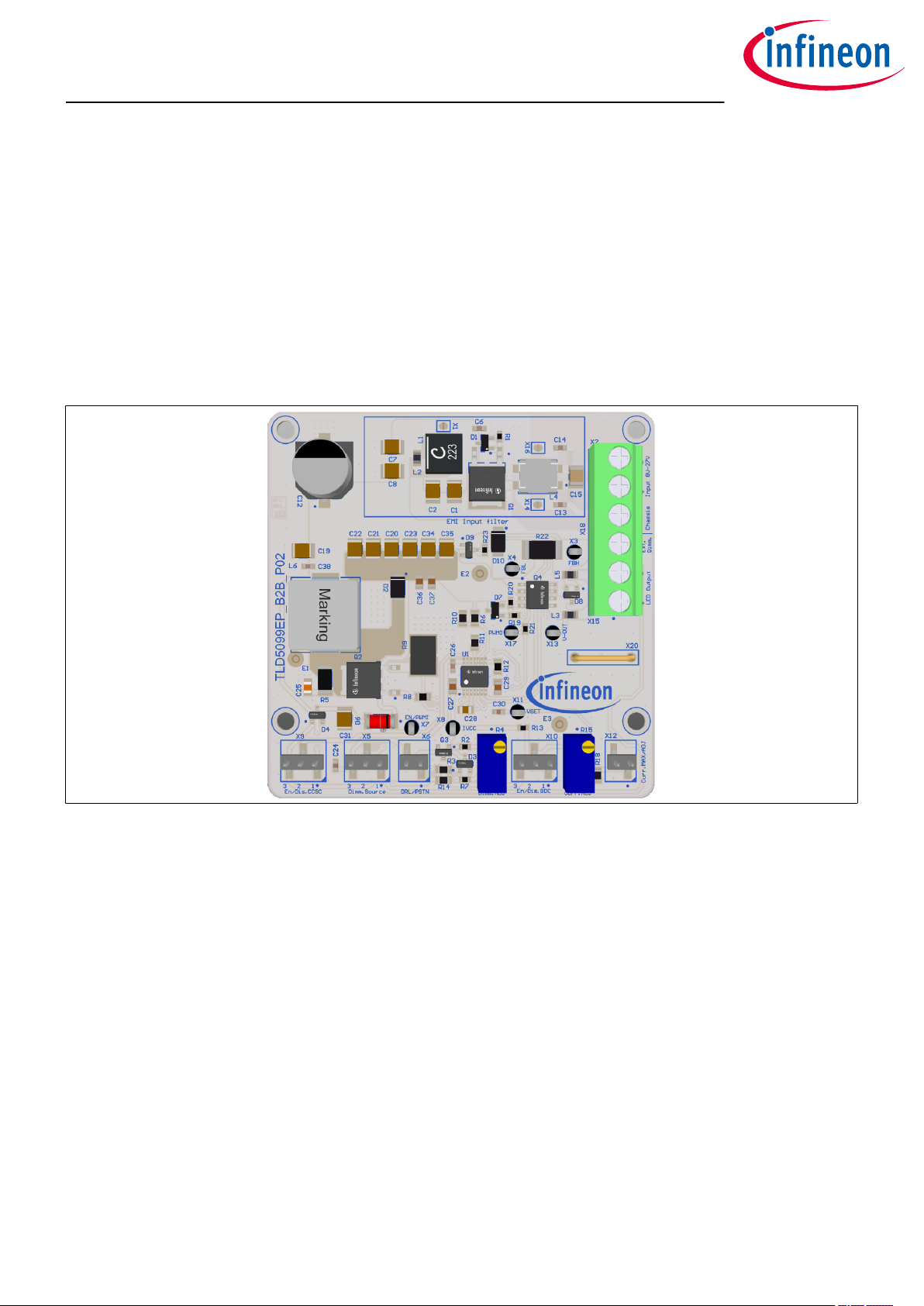
Evaluation board for high power LED application with TLD5099EP product in boost to battery topology.
Default configuration of the board is boost to battery topology without any additional features enabled. In this
configuration, it can deliver up to 21 W to the load with an eiciency above 84%. Auxiliary circuits, which protect
the DC-DC and the load during short to ground are present.
The board is also equipped with the following features that are enabled by jumpers:
• Output current adjustment trimmer
• Power derating circuitry
• Embedded PWM engine
• Cold crank survival circuit (CCSC)
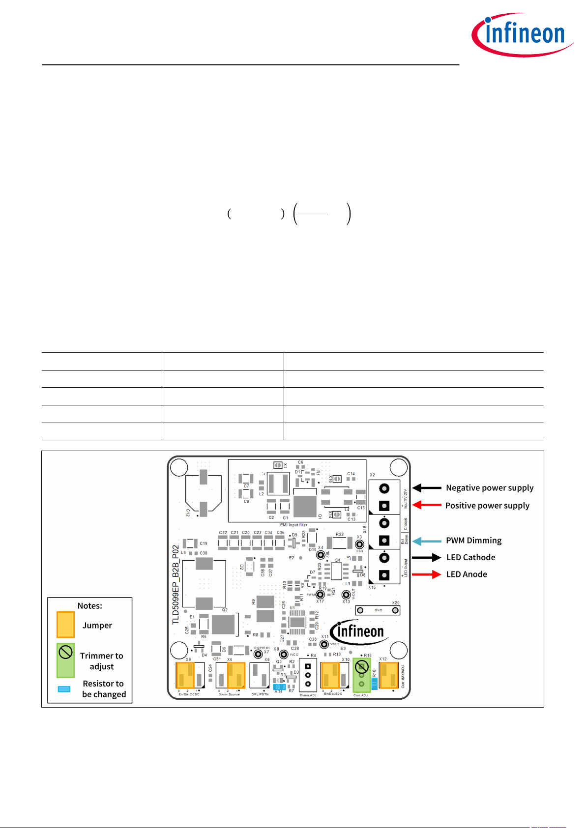
Figure 1 Board picture
User Manual 2
2021-01-18
Page 3
Boost to battery evaluation kit
TLD5099EP
1 Description
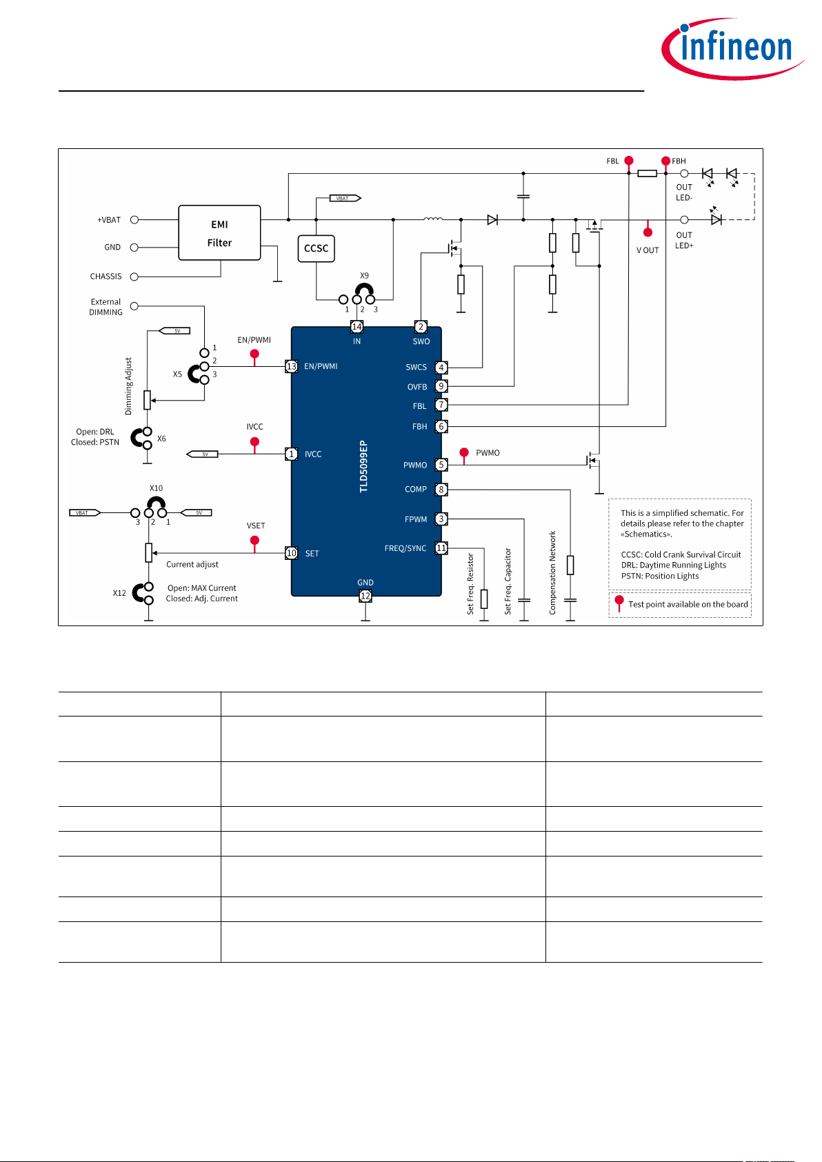
Figure 2 Simplified schematic
Table 1 Performance summary
Parameter Conditions Value
Input supply voltage Jumper X9 in position 2-3 (CCSC deactivated)
Parameter degradation below 6.5 V
Input supply voltage Jumper X9 in position 1-2 (CCSC active) 8 V to 27 V
Output current Jumper X12 open 1 A
Switching frequency VIN = 13.2 V; spread spectrum "on" 400 kHz
Eiciency Measured with 7 white standard LED 3 V @ 1 A
output current
Output voltage range Output voltage related to positive input 6 V to 23 V
Output overvoltage
protection
Output voltage related to ground 59 V
8 V to 27 V
Down to 6.5 V for less than 2 s
Down to 3.0 V for less than 2 s
> 84%
User Manual 3
2021-01-18
Page 4
Boost to battery evaluation kit
TLD5099EP
2 Quick start procedure
2 Quick start procedure
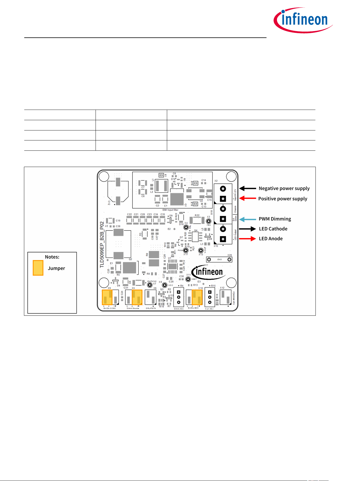
The default configuration of the board has all additional features disabled. In this configuration the output
current cannot be adjusted. The PWM signal has to be applied as digital signal on connector X18 (max. 45 V).
Jumpers are positioned as follows:
Table 2 Jumper position
Jumper number Condition Meaning
X9 Close 2-3 Disable CCSC
X5 Close 2-1 External dimming enabled
X10 Close 2-1 Disable battery dependent current
The default configuration is depicted below:
Figure 3 Default configuration of the board
User Manual 4
2021-01-18
Page 5
Boost to battery evaluation kit
TLD5099EP
3 Current adjustment
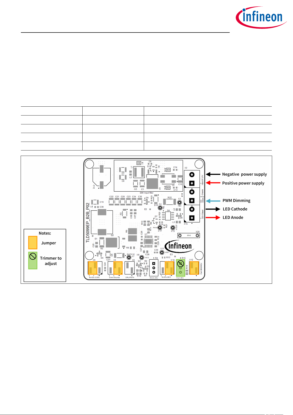
3 Current adjustment
The output current adjustment can be performed by changing the value of trimmer R15 with a screwdriver,
when X10 is closed in position 1-2 and X12 is closed. The output current can vary from 0 to 100% of the
maximum output current (in this evaluation board from 0 to 1 A). By removing jumper X12, the output current
will reach its maximum value. The PWM signal has to be applied as digital signal on connector X18 (max. 45 V).
Jumpers are positioned as follows:
Table 3 Jumper position
Jumper number Condition Meaning
X9 Close 2-3 Disable CCSC
X5 Close 2-1 External dimming enabled
X10 Close 2-1 Disable battery dependent current
X12 Closed Adjustable output current enabled
Figure 4 Current adjustment
User Manual 5
2021-01-18
Page 6
Boost to battery evaluation kit
TLD5099EP
4 Power derating (battery dependent current)
4 Power derating (battery dependent current)
The power derating acts by reducing V
(and thus the output current) when the battery voltage drops below
SET
8 V. It works better when R15 is trimmed to its maximum value. Otherwise a dierent derating profile is applied.
If a dierent derating profile is needed, R14 has to be changed. The aim is to have 1.6 V on pin SET when the
battery voltage reaches the desired threshold, below which the output current must decrease proportionally.
R14 can be calculated using:
R14 = R15 + R18 ⋅
BATT
1.6
− 1
(1)
V
where
• R15 = 10 kΩ
• R18 = 560 Ω
For example, if the power derating should start when the battery voltage drops under 12 V, R14 must be
replaced with a 68 kΩ 0603 resistor (please refer to the TLD5099EP datasheets for more information).
Jumpers are positioned as follows:
Table 4 Jumper position
Jumper number Condition Meaning
X9 Close 2-3 Disable CCSC
X5 Close 2-1 External dimming enabled
X10 Close 2-3 Enable battery dependent current
X12 Closed Adjustable output current enabled
Figure 5 Power derating
User Manual 6
2021-01-18
Page 7

Boost to battery evaluation kit
TLD5099EP
5 Embedded PWM engine
5 Embedded PWM engine
The embedded PWM engine provides an internal PWM signal without any external dimming signal required. It
is enabled when jumper X5 is closed in position 2-3. If jumper X6 is open, the EN/PWMI pin is biased at 5 V and
then the duty cycle is 100%. Closing jumper X6, the duty cycle is adjustable by means of trimmer R4. The PWM
frequency is set to 350 Hz. If another PWM frequency is needed, C28 must be changed to a proper value (please
refer to the TLD5099EP datasheets for more information).
Jumpers are positioned as follows:
Table 5 Jumper position
Jumper number Condition Meaning
X9 Close 2-3 Disable CCSC
X5 Close 2-3 Internal dimming enabled
X10 Close 2-1 Disable battery dependent current
X6 Closed Adjustable PWM dimming for position light
Figure 6 Embedded PWM engine
User Manual 7
2021-01-18
Page 8

Boost to battery evaluation kit
TLD5099EP
6 Cold crank survival circuit
6 Cold crank survival circuit
This feature helps the system to survive LV124 test E11 “severe test pulse”, when the input voltage drops below
4.5 V, which is the minimum input voltage for the TLD5099EP. This circuit feeds back the device with the output
voltage when the input voltage drops. To activate this feature, close jumper X9 in position 1-2. Other settings
can be le as preferred.
Note: The CCSC uses a Zener diode to adapt the output voltage to the required voltage for the TLD5099EP, so
that it can derate the eiciency performance.
Figure 7 Cold crank survival circuit
User Manual 8
2021-01-18
Page 9

1
1
2
2
3
3
4
4
5
5
6
6
7
7
8
8
D D
C C
B B
A A
08/01/2021 11:58:02Date:
Sheet of
Time:
© Infineon Technologies AG 2019. All Rights Reserved.
Author: Riccardo Zuin
03-TLD5099EP_B2B_S02_Input Filter.SchDoc
Infineon Technologies AG
IFI DC ATV BP
Via Niccolo Tommaseo 65b 35131 Padova Italy
S02
Title
Size: Rev.
A3
Document Name
03-TLD5099EP_B2B_S02_Input Filter.SchDoc
Rel.
REL
Variant
TLD5099EP_B2B
[No Variations]
Approved
<Appr.>
SVN Revision: Not in version control
GND
External Dimming
12
50V
C12
220uF
GND
2 3
1
Q1
IPD90P04P4L-04
R1
10k
GND GND
Vbat_FIL
4A PI type filter. Suitable for switching frequency down to 200kHz
N.M.
50V
C6
100nF
GND GND GND
MPZ2012S101ATD25
L2
100R
1 2
X1
Solder Jumper 2 Pins
GND
V bat
Ext_Dim
GND
1 2
X14
Solder Jumper 2 Pins
1 2
X16
Solder Jumper 2 Pins
50V
C14
470pF
50V
C13
470pF
1 4
2 3
ACM70V-701-2PL-TL00
L4
700R
Chassis
50V
C1
10uF
50VC210uF
50VC710uF
50VC810uF
50V
C15
4.7uF
XAL6060-103MEB
L1
10uH
MIN Input Voltage (V bat): 8V
TYP Input Voltage (V bat): 13,2V
MAX Input Voltage (V bat): 27V
MIN Input Voltage (V bat): 6.5V (for less than 2s)
1
2
Phoenix Contact
X18
1935776
1
2
Phoenix Contact
X2
1935776
31
NC
2
BZX84C10LT1G
D1
10V
Boost to battery evaluation kit
TLD5099EP
7 Schematics
7 Schematics
Figure 8 Input filter
User Manual 9
2021-01-18
Page 10

1
1
2
2
3
3
4
4
5
5
6
6
7
7
8
8
D D
C C
B B
A A
08/01/2021 11:59:11Date:
Sheet of
Time:
© Infineon Technologies AG 2019. All Rights Reserved.
Author: Riccardo Zuin
04-TLD5099EP_B2B_S02_Main Power.SchDoc
Infineon Technologies AG
IFI DC ATV BP
Via Niccolo Tommaseo 65b 35131 Padova Italy
S02
Title
Size: Rev.
A3
Document Name
04-TLD5099EP_B2B_S02_Main Power.SchDoc
Rel.
REL
Variant
TLD5099EP_B2B
[No Variations]
Approved
<Appr.>
SVN Revision: Not in version control
SWO
2
IVCC
1
SWCS
4
FPWM
3
EP
15
COMP8SET10FREQ/SYNC
11
FBH
6
PWMO
5
FBL
7
OVFB
9
GND
12
EN/PWMI13IN
14
U1
TLD5099EP
Vbat_FIL
50V
C26
100nF
GND
16V
C27
10uF
GND
R2
8.2k
123
R4
10k
R7
3.3k
GND
32
1
Q3
BSS138N
31
NC
2
D3
BAS16
GND
Vbat_FIL
IVCC(5V)
IVCC(5V)
Vbat_FIL
EN/PWMI
EN/PWMI
R3
2.2k
Set light, dimming and start-up circuit
Dimming Adjust
GND
Rfreq
GND
Cfpwm
(350Hz)
(400kHz Spread Spectrum ON)
1
2
X6
TSM-102-01-S-SV
Open: DRL
Closed: PSTN
1
2
3
X5
TSM-103-01-S-SV
Ext_Dim
(1-2) External Dimming
(2-3) Internal Dimming
VSET
1
2
X12
TSM-102-01-S-SV
123
R15
10k
GND
IVCC(5V)
Current Adjust
Open: MAX Current
Closed: Adj. Current
R13
22k
VSET
Set output continuous current
GND
C29
100nF
GND
50V
C19
10uF
GND
GND GND
12
D2
PMEG6030EP,115
50V
C20
10uF
50V
C21
10uF
50V
C22
10uF
0,8V
3,1V
0,1V
1,6V
PWR_Out
GND
PWMO
6-23V referred to V bat / 1A
2818R933mR
C28
560pF
0805
R10
1k
50V
C23
10uF
X3
5001
X4
5001
X8
5001 IVCC
FBH FBL
X11
5001
VSET
X7
5001
EN/PWMI
GND
GND
CCSC
123
X9
TSM-103-01-S-SV
Vbat_FIL
(3-2) Disable CCSC
(1-2) Enable CCSC
1
2
3
X10
TSM-103-01-S-SV
Vbat_FIL
(3-2) Enable V bat depending current
(1-2) Disable V bat depending current
FBH
FBL
0805
R6
47k
35V
C24
1uF
35V
C30
1uF
23
1
Q2
IPD22N08S2L-50
50V
C34
10uF
50V
C35
10uF
OVFB > 1,25V when V OUT > 59V
IVCC(5V)
PWR_Out
R12
0R
2010R52.2R
100V
C36
100nF
GND GND
50V
C38
100nF
GND
100V
C25
1nF
31
NC
2
D4
BAS16
Vbat_FIL
50V
C31
10uF
GND
CCSC
Cold Crank Survival Circuit (CCSC)
R11
2k
PWR_Out
GND
100V
C37
1uF
R8
0R
12
ZMY10-GS08D610V
SRP1265A-470M
L6
47uH
X20
D3082-05
0805
R14
39k
0805
R18
560R
Boost to battery evaluation kit
TLD5099EP
7 Schematics
Figure 9 Main power
User Manual 10
2021-01-18
Page 11

1
1
2
2
3
3
4
4
5
5
6
6
7
7
8
8
D D
C C
B B
A A
08/01/2021 12:10:05Date:
Sheet of
Time:
© Infineon Technologies AG 2019. All Rights Reserved.
Author: Riccardo Zuin
05-TLD5099EP_B2B_S02_Output Stage.SchDoc
Infineon Technologies AG
IFI DC ATV BP
Via Niccolo Tommaseo 65b 35131 Padova Italy
S02
Title
Size: Rev.
A3
Document Name
05-TLD5099EP_B2B_S02_Output Stage.SchDoc
Rel.
REL
Variant
TLD5099EP_B2B
[No Variations]
Approved
<Appr.>
SVN Revision: Not in version control
PWR_Out
PWMO
2
4
1
3
7, 8
5, 6
Q4A
BSO615CGHUMA1
R21
10R
GND
31
NC
2
BZX84C10LT1G
D7
10V
OUT LED+ (6-23V referred to V bat / 1A)
OUT LED-
X13
5001
V OUT
X17
5001
PWMO
MPZ2012S102ATD25
L5
1kR
MPZ2012S102ATD25
L3
1kR
R23
10k
31
NC
2
D9
BAS16
31
NC
2
D8
BAS16
1 2
D10
PMEG6030EP,115
Vbat_FIL
FBH
FBL
Suggested Output: Light White LEDs
LED Type: Seoul Semi WICOP-C
Number of LEDs in series: 2-7
LED part number: SWW0CS11S
2512
R22
300mR
1
2
Phoenix Contact
X15
1935776
R20
22k
R19
27k
Boost to battery evaluation kit
TLD5099EP
7 Schematics
Figure 10 Output stage
User Manual 11
2021-01-18
Page 12

Boost to battery evaluation kit
TLD5099EP
8 PCB layout
8 PCB layout
Figure 11 PCB layout top view
Figure 12 PCB layout bottom view
User Manual 12
2021-01-18
Page 13

Boost to battery evaluation kit
TLD5099EP
9 Bill of material
9 Bill of material
Table 6 Bill of material
Designator Value Manufacturer Manufacturer order
number
C1, C2, C7, C8, C19, C20,
C21, C22, C23, C31, C34,
C35
C6, C26, C38 100 nF AVX 06035C104K4Z2A
C12 220 uF Panasonic EEEFK1H221P
C13, C14 470 pF Murata GCM1885C1H471JA16
C15 4.7 uF Kemet C1210C475K5RACAUTO
C24, C30 1 uF TDK CGA3E1X7R1V105K080AC
C25 1 nF TDK Corporation CGA4F2X7R2A102M085AE
C27 10 uF TDK CGA4J1X7S1C106K125AC
C28 560 pF Murata GCM2165C2A561JA16
C29, C36 100 nF TDK CGA4J2X7R2A104M125AE
C37 1 uF TDK Corporation CGA4J3X7S2A105K125AB
D1, D7 10 V ON Semiconductor BZX84C10LT1G
D2, D10 PMEG6030EP,115 Nexperia PMEG6030EP,115
D3, D4, D8, D9 BAS16 Infineon Technologies BAS16
D6 10 V Vishay ZMY10-GS08
10 uF Murata GCM32EC71H106KA03
L1 10 uH Coilcra XAL6060-103MEB
L2 100 Ω TDK Corporation MPZ2012S101ATD25
L3, L5 1 kΩ TDK MPZ2012S102ATD25
L4 - TDK ACM70V-701-2PL-TL00
L6 47 uH Bourns SRP1265A-470M
Q1 IPD90P04P4L-04 Infineon Technologies IPD90P04P4L-04
Q2 IPD22N08S2L-50 Infineon Technologies IPD22N08S2L-50
Q3 BSS138N Infineon Technologies BSS138N
Q4 BSO615CGHUMA1 Infineon Technologies BSO615CGHUMA1
R1, R23 10 kΩ Vishay CRCW060310K0FK
R2 8.2 kΩ Vishay CRCW06038K20FK
R3 2.2 kΩ Vishay CRCW08052K20FK
R4, R15 10 kΩ Vishay T93YA103KT20
R5 2.2 Ω Vishay CRCW20102R20FK
R6 47 kΩ Vishay CRCW080547K0FK
R7 3.3 kΩ Vishay CRCW06033K30FK
R8, R12 0 Ω Yageo AC0805JR-070RL
R9 33 mΩ Vishay WSHM2818R0330FEA
User Manual 13
2021-01-18
Page 14

Boost to battery evaluation kit
TLD5099EP
9 Bill of material
Table 6 Bill of material (continued)
Designator Value Manufacturer Manufacturer order
number
R10 1 kΩ Vishay CRCW08051K00FK
R11 2 kΩ Vishay CRCW08052K00FK
R13, R20 22 kΩ Vishay CRCW060322K0FK
R14 39 kΩ Vishay CRCW080539K0FK
R18 560 Ω Vishay CRCW0805560RFK
R19 27 kΩ Vishay CRCW060327K0FK
R21 10 Ω Vishay CRCW060310R0FK
R22 300 mΩ Vishay WSL2512R3000FEA
U1 TLD5099EP Infineon Technologies TLD5099EP
X1, X14, X16 Solder Jumper 2 Pins - Solder Jumper 2 Pins
X2, X15, X18 1935776 Phoenix Contact 1935776
X3, X4, X7, X8, X11, X13, X17 5001 Keystone 5001
X5, X9, X10 TSM-103-01-S-SV Samtec TSM-103-01-S-SV
X6, X12 TSM-102-01-S-SV Samtec TSM-102-01-S-SV
X20 D3082-05 Harwin D3082-05
User Manual 14
2021-01-18
Page 15

Boost to battery evaluation kit
TLD5099EP
10 Eiciency measurements
10 Eiciency measurements
Figure 13 Eiciency vs. input voltage
This eiciency performance has been obtained with:
Table 7 Parameters influencing eiciency
Output load: Series of 7 white standard LED with Vj = 3 V kept cooled with forced air
EMI filter: Totally bypassed by closing the jumpers X1, X14 and X16
CCSC: O (jumper X9 closed on 2-3)
Current adjustment: O (jumper X12 le open)
Dimming output: O (jumper X6 le open)
Power derating: O (jumper X10 closed on 1-2)
Eiciency performances can be increased: refer to Chapter 11.
User Manual 15
2021-01-18
Page 16

Boost to battery evaluation kit
TLD5099EP
11 Maximizing eiciency
11 Maximizing eiciency
This evaluation board has been designed to reach a fair compromise between eiciency performance and EM
emissions compliance.
Nevertheless, if the maximum eiciency is needed, the following actions should be considered:
1. Remove the snubber circuit R5, C25 or choose a lower value for the capacitor C25 (for example, 470 pF)
2. Bypass the whole EMI filter by bridging the jumpers X1, X14 and X16
3. Bypass the output ferrite beads L3 and L5
4. Replace the main inductor L6 with one that boasts a lower parasitic DC resistance, for example,
• Vishay IHLP6767GZER470M8A
• Bourns SRP1770TA-470M
5. Turn o the CCSC by placing jumper X9 on position 2-3
6. Bypass gate resistor R8
User Manual 16
2021-01-18
Page 17

Boost to battery evaluation kit
TLD5099EP
12 Minimizing EM emissions
12 Minimizing EM emissions
This evaluation board has been designed to reach a fair compromise between eiciency performance and EM
conducted emissions compliance. Furthermore, this evaluation board can fulfill the class V of the CISPR25 in
conducted emissions from 150 kHz to 108 MHz.
Nevertheless, if the minimum EM emission is required, the following actions should be considered:
1. Choose a higher value for the capacitor C25 (for example, 2.2 nF)
2. Include the whole EMI filter by removing bridges from the jumpers X1, X14 and X16
3. Replace the 0 Ω resistor R8 with a higher value such as 10 Ω or 22 Ω
4. Replace the main inductor L6 with a shielded one (for example, Cyntec VCHE106G-470MS6) and connect
the shield to ground
5. Connect the CHASSIS TERMINAL with a short piece of wire as close as possible to the test ground plane
where the board is placed
User Manual 17
2021-01-18
Page 18

Boost to battery evaluation kit
TLD5099EP
13 Revision history
13 Revision history
Table 8 Revision history
Document version Date of release Description of changes
Rev. 1.00 2020-01-29 Initial release. Matching to evalboard S01_P01.
Rev. 2.00 2021-01-18 Matching to evalboard S02_P02:
• Connectors re-arranged
• Added ground bar
User Manual 18
2021-01-18
Page 19

Trademarks
All referenced product or service names and trademarks are the property of their respective owners.
Edition 2021-01-18
Published by
Infineon Technologies AG
81726 Munich, Germany
©
2021 Infineon Technologies AG
All Rights Reserved.
Do you have a question about any
aspect of this document?
Email: erratum@infineon.com
Document reference
IFX-awj1578581807661
IMPORTANT NOTICE
The information contained in this application note is
given as a hint for the implementation of the product
only and shall in no event be regarded as a description
or warranty of a certain functionality, condition
or quality of the product. Before implementation
of the product, the recipient of this application
note must verify any function and other technical
information given herein in the real application.
Infineon Technologies hereby disclaims any and all
warranties and liabilities of any kind (including without
limitation warranties of non-infringement of intellectual
property rights of any third party) with respect to any
and all information given in this application note.
The data contained in this document is exclusively
intended for technically trained sta. It is the
responsibility of customer’s technical departments to
evaluate the suitability of the product for the intended
application and the completeness of the product
information given in this document with respect to such
application.
WARNINGS
Due to technical requirements products may contain
dangerous substances. For information on the types
in question please contact your nearest Infineon
Technologies oice.
Except as otherwise explicitly approved by Infineon
Technologies in a written document signed by
authorized representatives of Infineon Technologies,
Infineon Technologies’ products may not be used in
any applications where a failure of the product or
any consequences of the use thereof can reasonably
be expected to result in personal injury.
 Loading...