

Page 1
User Manual Please read the Important Notice and Warnings at the end of this document Rev.1.00
www.infineon.com page 1 of 14 2020-12-03
Z8F80036493
TLD2252-2EP rear combination lamp evaluation
board
User Manual
About this document
Scope and purpose
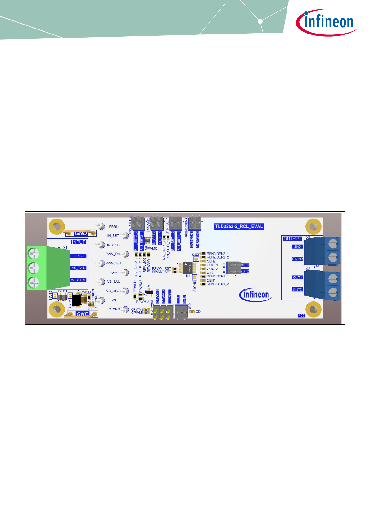
The purpose of the TLD2252-2EP rear combination lamp evaluation board (TLD2252-2_RCL_EVAL) board is to
help designers evaluate the features and the performance of the TLD2252-2EP, a two-channel linear current
source LED driver for automotive LED lighting applications. TLD2252-2EP provides a simple and compact
solution for the implementation of a rear combination lamp (RCL).
This user manual provides the usage instructions of the TLD2252-2 _RCL_ EVAL board (schematic version S00,
PCB version P00).
Figure 1 TLD2252-2_RCL_EVAL board
Intended audience
Hardware engineers, system architects.
Page 2
User Manual 2 of 14 Rev.1.00
2020-12-03
TLD2252-2EP rear combination lamp evaluation board
User Manual
TLD2252-2_RCL_EVAL description
Related information
Table 1 Supplementary links and document references
Reference
Description
LITIX™ Basic+ TLD2252-2EP
product home page
Product website which contains reference information for the LITIX™ Basic+
TLD2252-2EP including datasheet, application notes, simulation models,
boards and relevant training
LITIX™ Basic+ family website
All information about LITIX™ Basic+ family products
LITIX™ Basic+ LED driver
family: How to implement a
rear combination lamp
Application note regarding the main operating principles of the pulse width
modulation (PWM) engine integrated into the LITIX™ Basic+ TLD2252-2EP,
TLD2141-3EP and TLD2142-1EP, and how to build a rear combination lamp
(RCL) using PWM
LITIX™ Basic+ LED driver
family: Diagnosis and fault
management
Application note regarding the main operating principles of the diagnosis
and fault management features integrated in the LITIX™ Basic+ family.
LITIX™ Basic+ Boards
Available evaluation boards for LITIX™ Basic+
LED rear lighting - application
page
Application website for rear LED lighting
Table of contents
About this document ......................................................................................................................... 1
Table of contents .............................................................................................................................. 2
1 TLD2252-2_RCL_EVAL description .............................................................................................. 3
1.1 Key features ............................................................................................................................................. 3
1.2 Connectors and jumpers ......................................................................................................................... 4
1.3 On-board load ......................................................................................................................................... 5
1.4 Test points ............................................................................................................................................... 6
2 Quick start ............................................................................................................................... 7
3 Schematics, layout and bill of material ...................................................................................... 8
3.1 Schematics .............................................................................................................................................. 8
3.2 Layout .................................................................................................................................................... 10
3.3 Bill of materials ...................................................................................................................................... 11
3.4 PCB design data .................................................................................................................................... 12
Revision history ...............................................................................................................................13
Page 3
User Manual 3 of 14 Rev.1.00
2020-12-03
TLD2252-2EP rear combination lamp evaluation board
User Manual
TLD2252-2_RCL_EVAL description
1 TLD2252-2_RCL_EVAL description
The TLD2252-2_RCL_EVAL is an evaluation board equipped with one LITIX™ Basic+ TLD2252-2EP and on-board
LEDs for easy evaluation of an RCL application when realized with use of the TLD2252-2EP pulse width
modulation (PWM) engine.
The board can be used within the typical automotive voltage range, 8 V to 16 V. It gives the user the freedom to
evaluate all of the TLD2252-2EP features and possible configurations by setting the necessary jumpers
accordingly.
As the PWM-engine of LITIX™ Basic+ TLD2252-2EP can be used to drive other LITIX™ Basic+ devices, the
TLD2252-2_RCL_EVAL board can be used in combination with the BASICPLUS_DEMOBOARD for combined
family evaluation.
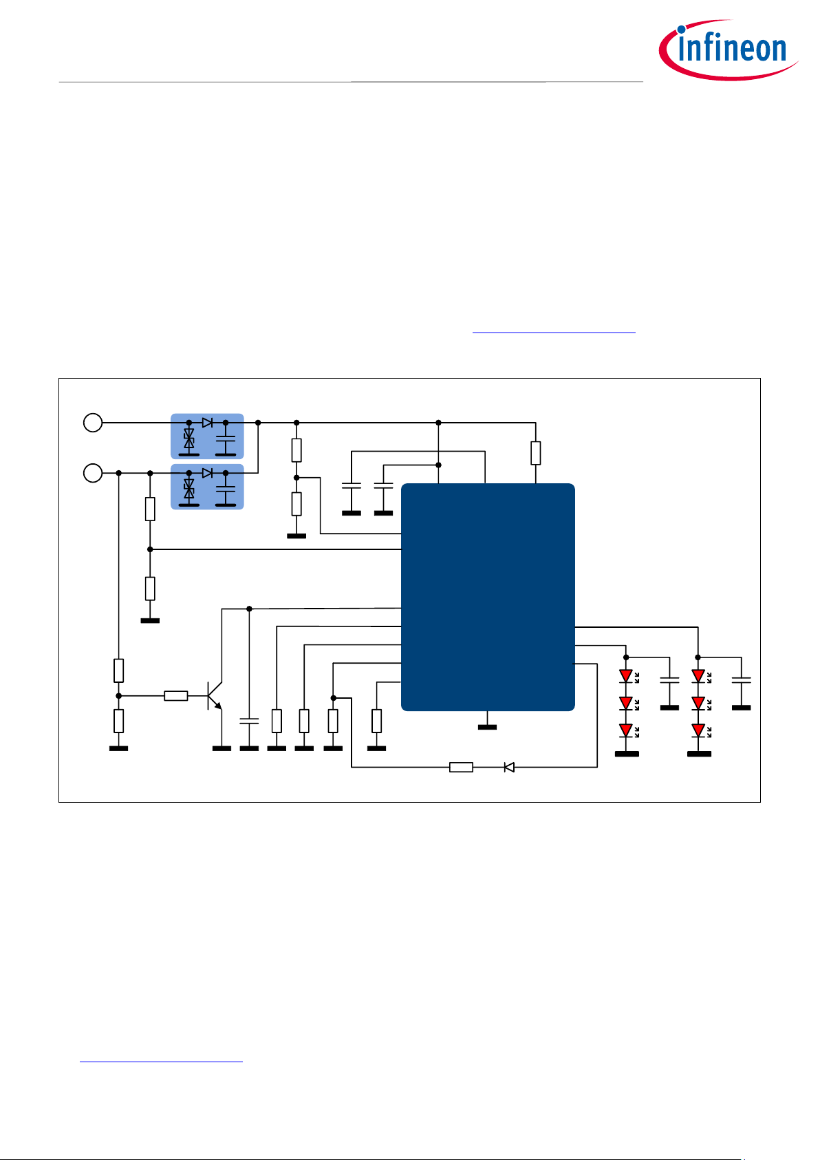
Figure 2 Rear combination lamp implemented with LITIX™ Basic+ TLD2252-2EP
1.1 Key features
The TLD2252-2_RCL_EVAL has the following features:
1. Equipped with one LITIX™ Basic+ TLD2252-2EP
2. Typical supply voltage range 8 V to 16 V
3. Equipped with jumpers for evaluation of the features in different configurations (e.g. PWM-engine)
4. On-board LED load, 3 LEDs per output channel
5. Possibility to connect external load
6. Possibility to drive other LITIX™ Basic+ devices with PWM-signal, in combination with
BASICPLUS_DEMOBOARD
7. 11.4 cm x 4.2 cm 2-layer PCB
OUT1
OUT2
TLD2252-2EP
VS
D
EN/DEN1
ERRN
IN_SET1
C
VS
*
C
D
R
SET1
R
EN/DEN2
V
STOP
R
EN/DEN1
R
ERRN
* For EMI improvement,
if required (e.g. 4,7 or 10nF)
PWMO
PWM_SET
GND
R
PWM_SET
R
PWM_RST
PWM_RST
PWMI
C
PWMI
V
TAIL
EN/DEN2
IN_SET2
Supply
Protection
R
SET2
R
EN/DEN2_2
R
EN/DEN1_2
C
OUT
*
C
OUT
*
R
PWMO
Page 4

User Manual 4 of 14 Rev.1.00
2020-12-03
TLD2252-2EP rear combination lamp evaluation board
User Manual
TLD2252-2_RCL_EVAL description
1.2 Connectors and jumpers
The TLD2252-2_RCL_EVAL board connectors are described in Table 2.
Table 2 TLD2252-2_RCL_EVAL connectors
Connector
Description
INPUT
VS_STOP
Power supply, typical 8 V to 16 V, and deactivation of the internal PWM engine of the
LITIX™ Basic+ TLD2252-2EP
VS_TAIL
Power supply, typical 8 V to 16 V, and activation of the internal PWM engine of the
LITIX™ Basic+ TLD2252-2EP
GND
Ground
OUTPUT
GND
Ground
PWMO
LITIX™ Basic+ TLD2252-2EP PWM signal to drive other LITIX™ Basic devices
OUT1
External load for output channel 1, OUT1
OUT2
External load for output channel 2, OUT2
The TLD2252-2_RCL_EVAL board jumpers are described in Table 3.
Table 3 TLD2252-2_RCL_EVAL board jumpers
Jumper
Description and configuration
JPN_SET1
Sets the output current of OUT1:
• RIN_SET1_1 (36.5 kΩ): sets the output current to 10 mA
• RIN_SET1_2 (7.32 kΩ): sets the output current to 50 mA
JPPWMO
PWM output enable:
• IN_SET1: enables PWM at OUT1
• IN_SET2: enables PWM at OUT2
JPN_SET2
Sets the output current of OUT2:
• RIN_SET2_1 (14.7 kΩ): sets the output current to 50 mA
• RIN_SET2_2 (7.32 kΩ): sets the output current to 100 mA
JPEN2/DEN2
Activate the device and diagnosis for OUT2:
• EN1/DEN1: use the resistor divider on EN1/DEN1 (REN1/DEN1_1) to activate OUT2
• EN2/DEN2: use separate resistor divider EN1/DEN1 (REN1/DEN1_1) to activate
OUT2. During tail function (board supplied via VS_TAIL), place jumper on
EN1/DEN1 position
JPOUT
On board load connection
• OUT1: connects OUT1 to on-board load
• OUT2: connects OUT2 to on-board load
JPD
Diagnosis management
• GND: when a fault is detected only the channel under fault condition will be
deactivated. The error will be communicated via ERRN
Page 5
User Manual 5 of 14 Rev.1.00
2020-12-03
TLD2252-2EP rear combination lamp evaluation board
User Manual
TLD2252-2_RCL_EVAL description
Jumper
Description and configuration
• Open: when a fault is detected both channels will switch off
• CD: when a fault is detected both channels will switch off after a delay time t
D(set)
.
Delay time is set by CD capacitor
JPPWMI
PWMI connection
• CPWMI1 (120 nF): sets the PWM frequency to 220 Hz and duty cycle 10%
• CPWMI2 (68 nF): sets the PWM frequency to 400 Hz and duty cycle 10%
• GND: duty cycle is 100%
The duty cycle is set by the RPWM_SET (4.53 kΩ) and RPWM_RST (41.2 kΩ) resistors
JPOUT
On board load connection
• OUT1: connects OUT1 to on-board load. Leave open to connect to external load
• OUT2: connects OUT2 to on-board load. Leave open to connect to external load
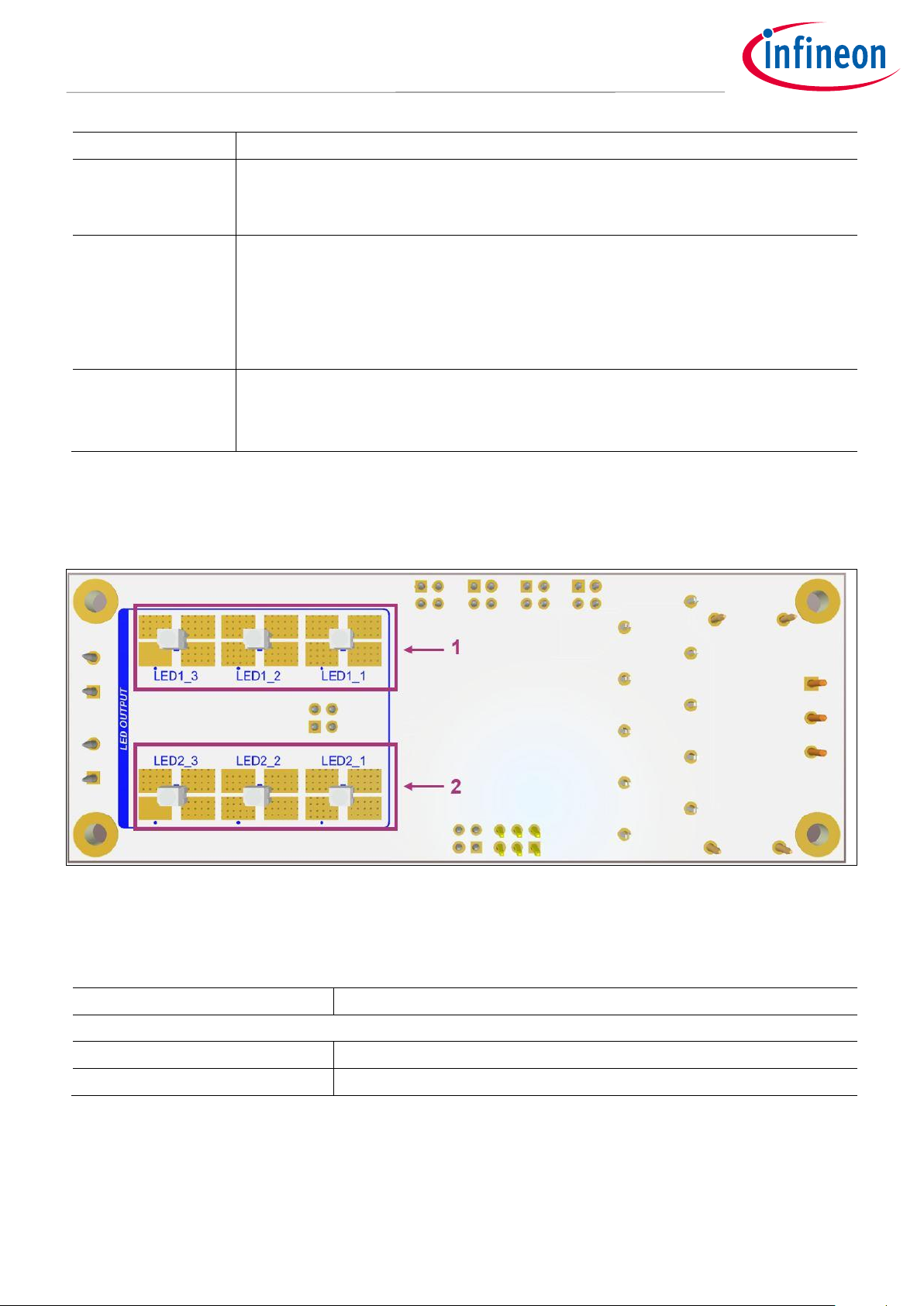
1.3 On-board load
The TLD2252-2_RCL_EVAL board is equipped with on-board LED load (on the bottom side) for easy evaluation.
Figure 3 On-board LED load
The on-board LED load shown in Figure 3 is described in Table 4.
Table 4 On-board LED load
Load
Description
LED OUTPUT
Load 1
3 x 1 LEDs in series; used when OUT1 of JPOUT is bypassed
Load 2
3 x 1 LEDs in series; used when OUT2 of JPOUT is bypassed
Page 6

User Manual 6 of 14 Rev.1.00
2020-12-03
TLD2252-2EP rear combination lamp evaluation board
User Manual
TLD2252-2_RCL_EVAL description
1.4 Test points
The TLD2252-2_RCL_EVAL board is equipped with several test points and two ground terminals for easy
monitoring of significant voltages, Figure 4.
Figure 4 Test points and ground terminals
Page 7

User Manual 7 of 14 Rev.1.00
2020-12-03
TLD2252-2EP rear combination lamp evaluation board
User Manual
Quick start
2 Quick start
• Connect a voltage source to VS_TAIL or VS_STOP and GND, typical 8 V to 16 V
• Select the output current by placing jumpers at JPN_SET1 and JPN_SET2
• Configure the diagnosis management at JPD
• Select if PWM will be used by placing a jumper at JPPWMI (only available when suppy at VS_TAIL)
• Select the output channels that will driven by the PWM engine by placing a jumper at JPPWMO (only
available when suppy at VS_TAIL)
• Enable output channel 2 by placing a jumper at JPEN/DEN2 (when suppy at VS_TAIL, bypass EN1/DEN1)
• Select load by bypassing OUT1 and OUT2 of JPOUT in order to use the on-board LED load
Page 8
User Manual 8 of 14 Rev.1.00
2020-12-03
TLD2252-2EP rear combination lamp evaluation board
User Manual
Schematics, layout and bill of material
3 Schematics, layout and bill of material
For the calculation of the external components required for the LITIX™ Basic+ TLD2252-2EP and used on the
TLD2252-2_RCL_EVAL board refer to the following documentation:
• LITIX™ Basic+ TLD2252-2EP data sheet
• LITIX™ Basic+ LED driver family: How to implement a rear combination lamp
• LITIX™ Basic+ LED driver family: Diagnosis and fault management
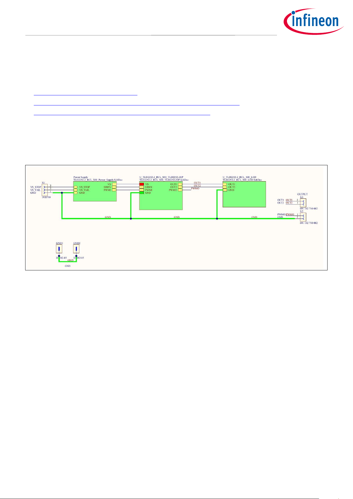
3.1 Schematics
In Figure 5, the top-level schematic of the TLD2252-2_RCL_EVAL board is shown. Figure 6, Figure 7 and Figure 8
show the schematic of the power supply circuit, the TLD2252-2EP and the on-board LED load respectively.
Figure 5 Schematic of TLD2252-2_RCL_EVAL board – top level
Page 9

User Manual 9 of 14 Rev.1.00
2020-12-03
TLD2252-2EP rear combination lamp evaluation board
User Manual
Schematics, layout and bill of material
Figure 6 Schematic of TLD2252-2_RCL_EVAL board – power supply
Figure 7 Schematic of TLD2252-2_RCL_EVAL board – TLD2252-2EP
Page 10
User Manual 10 of 14 Rev.1.00
2020-12-03
TLD2252-2EP rear combination lamp evaluation board
User Manual
Schematics, layout and bill of material
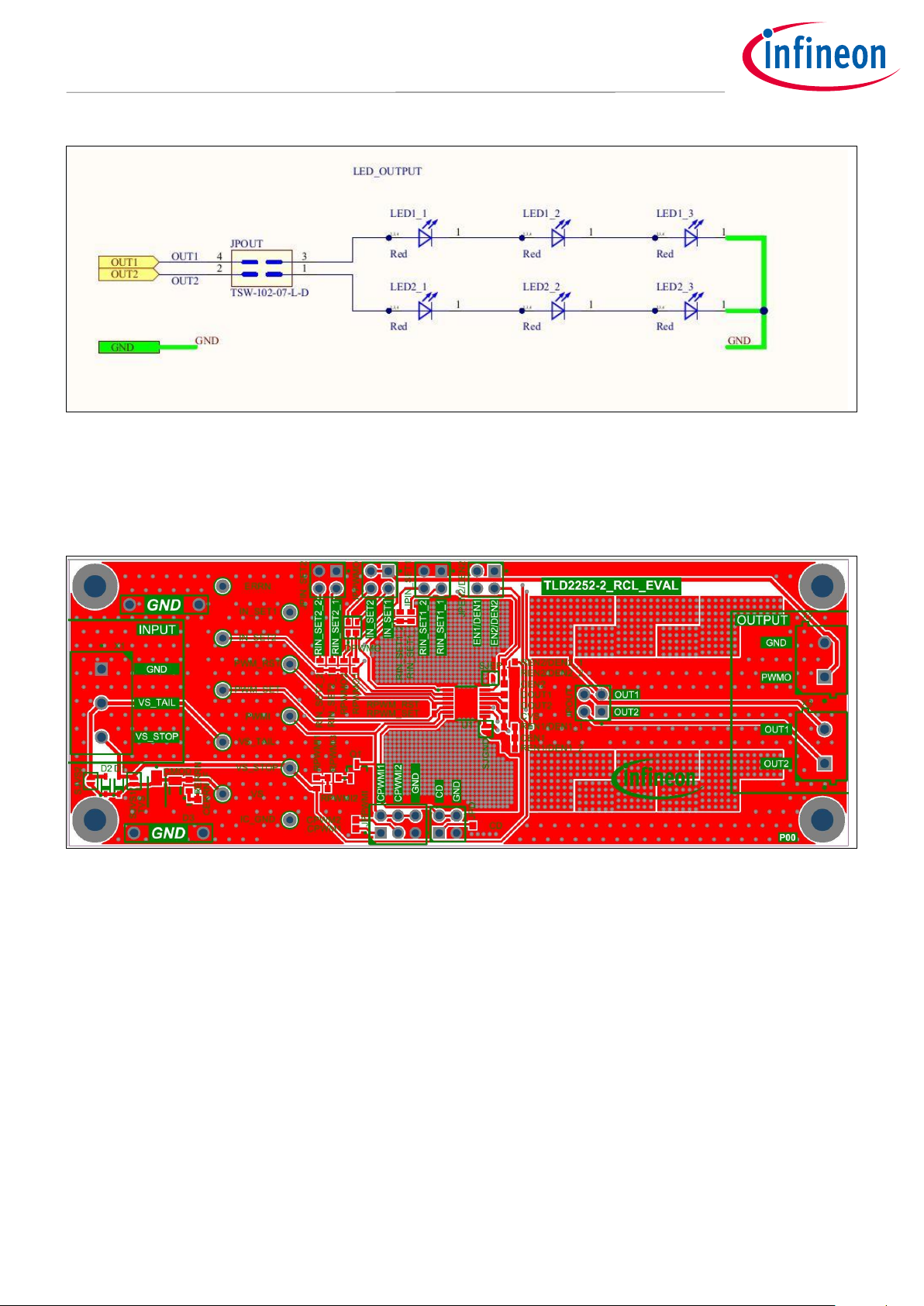
Figure 8 Schematic of TLD2252-2_RCL_EVAL board – on-board LED load
3.2 Layout
Figure 9 and Figure 10 show the layout of the TLD2252-2_RCL_EVAL board.
Figure 9 Layout of TLD2252-2_RCL_EVAL board – top layer
Page 11

User Manual 11 of 14 Rev.1.00
2020-12-03
TLD2252-2EP rear combination lamp evaluation board
User Manual
Schematics, layout and bill of material
Figure 10 Layout of TLD2252-2_RCL_EVAL board – bottom layer
3.3 Bill of materials
Table 5 shows theTLD2252-2_RCL_EVAL board bill of material.
Table 5 Bill of material
Designator
Value
Manufacturer
Manufacturer order number
CD, CERRN_F, COUT1,
COUT2, CVS
10 nF
AVX
06035F103K4Z2A
CEN1, CEN2
10 nF
MuRata
GCM188R71H103JA37
CMOD
2.2 μF
MuRata
GRM31CR71H225KA88
CPWM1
120 nF
Kemet
C0603C124K4RACTU
CPWM2
68nF
Kemet
C0603C683M4RACTU
D1, D2
BAT165
Infineon Technologies AG
BAT165
D3
5.60V
Vishay
BZX584C5V6-V-G
DPWMO
BAS40-07W
Infineon Technologies AG
BAS40-07W
ERRN, IC_GND, IN_SET1,
IN_SET2, PWM_RST,
PWM_SET, PWMI, VS,
VS_STOP, VS_TAIL
5002
Keystone Electronics
Corp.
5002
GND1, GND2
D3082-05
Harwin
D3082-05
JPD, JPEN2/DEN2,
JPIN_SET1, JPIN_SET2,
JPOUT, JPPWMO
TSW-102-07-L-D
Samtec
TSW-102-07-L-D
JPPWMI
TSW-103-08-G-D
Samtec
TSW-103-08-G-D
LED1_1, LED1_2, LED1_3,
LED2_1, LED2_2, LED2_3
Red
OSRAM Opto
Semiconductors
Q65110A4135
Q1
BC846ALT1G
ON Semiconductor
BC846ALT1G
REN1/DEN1_1,
REN2/DEN2_1, RPWMI1,
RPWMI3
10k
Yageo
RC0603FR-0710KL
Page 12

User Manual 12 of 14 Rev.1.00
2020-12-03
TLD2252-2EP rear combination lamp evaluation board
User Manual
Schematics, layout and bill of material
Designator
Value
Manufacturer
Manufacturer order number
REN1/DEN1_2,
REN2/DEN2_2, RPWMI2
3.6k
Yageo
AC0603FR-073K6L
RERRN
20k
Yageo
AC0603JR-0720KL
RIN_SET1_1
36.5k
Vishay
CRCW060336K5FK
RIN_SET1_2,
RIN_SET2_2, RPWMO1,
RPWMO2
7.32k
Vishay
CRCW06037K32FK
RIN_SET2_1
14.7k
Vishay
CRCW060314K7FK
RPWM_RST
41.2k
Vishay
CRCW060341K2FK
RPWM_SET
4.53k
Vishay
CRCW06034K53FK
SJEP, SJGND, SJVS1,
SJVS2
Solder Jumper 2
Pins
Infineon Technologies AG
Solder Jumper 2 Pins
TVS
SMAJ30CA
Littelfuse
SMAJ30CA
U1
TLD2252-2EP
Infineon Technologies AG
TLD2252-2EP
X1
1935789
Phoenix Contact
1935789
X2, X3
691 102 710 002
Wurth Elektronik
691 102 710 002
3.4 PCB design data
The Altium project is available on the TLD2252-2_RCL_EVAL website.
Page 13

User Manual 13 of 14 Rev.1.00
2020-12-03
TLD2252-2EP rear combination lamp evaluation board
User Manual
Revision history
Revision history
Document
version
Date of release
Description of changes
Rev.1.00
2020-12-03
Initial release
Page 14

Trademarks
All referenced product or service names and trademarks are the property of their respective owners.
Edition 2020-12-03
Z8F80036493
Published by
Infineon Technologies AG
81726 Munich, Germany
© 2020 Infineon Technologies AG.
All Rights Reserved.
Do you have a question about this
document?
Email: erratum@infineon.com
Document reference
IMPORTANT NOTICE
The information contained in this application note is
given as a hint for the implementation of the product
only and shall in no event be regarded as a
description or warranty of a certain functionality,
condition or quality of the product. Before
implementation of the product, the recipient of this
application note must verify any function and other
technical information given herein in the real
application. Infineon Technologies hereby disclaims
any and all warranties and liabilities of any kind
(including without limitation warranties of noninfringement of intellectual property rights of any
third party) with respect to any and all information
given in this application note.
The data contained in this document is exclusively
intended for technically trained staff. It is the
responsibility of customer’s technical departments
to evaluate the suitability of the product for the
intended application and the completeness of the
product information given in this document with
respect to such application.
For further information on the product, technology,
delivery terms and conditions and prices please
contact your nearest Infineon Technologies office
(www.infineon.com).
WARNINGS
Due to technical requirements products may contain
dangerous substances. For information on the types
in question please contact your nearest Infineon
Technologies office.
Except as otherwise explicitly approved by Infineon
Technologies in a written document signed by
authorized representatives of Infineon
Technologies, Infineon Technologies’ products may
not be used in any applications where a failure of the
product or any consequences of the use thereof can
reasonably be expected to result in personal injury.
 Loading...