

Page 1
User Manual Please read the Important Notice and Warnings at the end of this document V 1.0
www.infineon.com page 1 of 11 2021-01-13
Z8F80042284
TLD1211SJ evaluation board
User Manual
About this document
Scope and purpose
The scope of the TLD1211SJ_EVAL (evaluation) board is to help designers evaluate the performance of the
LITIX™ Linear TLD1211SJ, a single channel linear current source LED driver for automotive LED lighting
applications. The LITIX™ Linear TLD1211SJ provides a simple and low-cost solution for low current applications
up to 85 mA. When using additional external power stages as “booster” transistors, it can also be used to drive
high currents up to 2.5 A.
This user manual provides the usage instructions of the TLD1211SJ_EVAL board (schematic version
S00, PCB version P00).
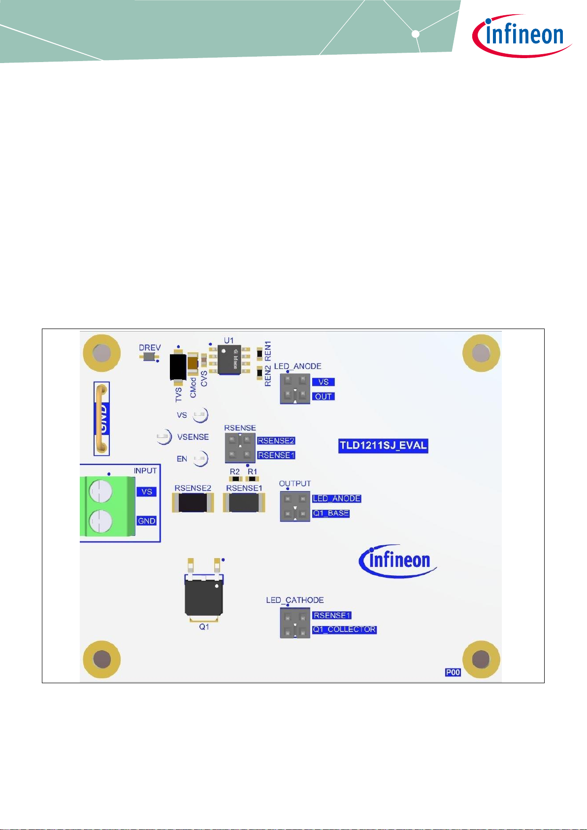
Figure 1 TLD1211SJ_EVAL board
Intended audience
Hardware engineers, system architects
Page 2

User Manual Please read the Important Notice and Warnings at the end of this document V 1.0
www.infineon.com page 2 of 11 2021-01-13
TLD1211SJ evaluation board
User Manual
TLD1211SJ_EVAL description
Related information
Table 1 Supplementary links and document references
Reference
Description
LITIX™ Linear TLD1211SJ product
Product website which contains reference information for
the LITIX™ Linear TLD1211SJ including datasheet,
simulation models, board and relevant trainings
LITIX™ Linear family
All information about LITIX™ Linear family products
LED driving concepts and Linear LED drivers
Application note regarding the usage and design-in of the
LITIX™ Linear and BCR LED drivers
LED rear lighting - application
Application website for rear LED lighting
Table of contents
About this document ......................................................................................................................... 1
Table of contents .............................................................................................................................. 2
1 TLD1211SJ_EVAL description .................................................................................................... 3
1.1 Key features ............................................................................................................................................. 4
1.2 Connectors and jumpers ......................................................................................................................... 4
1.3 On-board load ......................................................................................................................................... 5
1.4 Test points ............................................................................................................................................... 5
2 Quick start ............................................................................................................................... 6
2.1 Low current configuration, I
OUT
= 50 mA ................................................................................................. 6
2.2 High current configuration, I
OUT
= 300 mA .............................................................................................. 6
3 Schematics, layout and bill of material ...................................................................................... 7
3.1 Schematics .............................................................................................................................................. 7
3.2 Layout ...................................................................................................................................................... 8
3.3 Bill of materials ........................................................................................................................................ 9
3.4 PCB design data ...................................................................................................................................... 9
Revision history ...............................................................................................................................10
Page 3
User Manual Please read the Important Notice and Warnings at the end of this document V 1.0
www.infineon.com page 3 of 11 2021-01-13
TLD1211SJ evaluation board
User Manual
TLD1211SJ_EVAL description
1 TLD1211SJ_EVAL description
The TLD1211SJ_EVAL is an evaluation board equipped with one LITIX™ Linear TLD1211SJ and on-board LEDs
for easy evaluation. The board can be used within the typical automotive voltage range, 8 V to 16 V. The
jumpers available on the board offer the user the possibility to evaluate the LITIX™ Linear TLD1211SJ in both
low and high current applications.
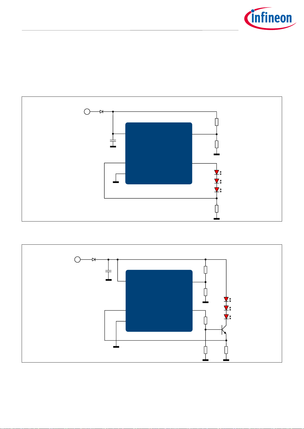
Figure 2 Low current application with LITIX™ Linear TLD1211SJ
Figure 3 High current application with LITIX™ Linear TLD1211SJ and “booster” transistor
TLD1211SJ
VSENSE
VS
EN
GND
OUT
R
SENSE
V
S
R
EN2
R
EN1
TLD1211SJ
VSENSE
VS
EN
GND
OUT
R
SENSE
V
S
R
EN2
R
EN1
Page 4

User Manual Please read the Important Notice and Warnings at the end of this document V 1.0
www.infineon.com page 4 of 11 2021-01-13
TLD1211SJ evaluation board
User Manual
TLD1211SJ_EVAL description
1.1 Key features
The TLD1211SJ_EVAL has the following features:
• Equipped with one LITIX™ Linear TLD1211SJ
• Typical supply voltage range 8 V to 16 V
• Equipped with jumpers that provide the possibility to evaluate TLD1211SJ in two different current
configurations:
o I
OUT
= 50 mA
o I
OUT
= 300 mA
• On-board LED load, 3 red LEDs
• 7.4 cm x 6.1 cm 2-layer PCB
1.2 Connectors and jumpers
The TLD1211SJ_EVAL board connectors are described in Table 2.
Table 2 TLD1211SJ_EVAL connectors
Connector
Description
INPUT
VS
Power supply, typical 8 V to 16 V
GND
Ground
The TLD1211SJ_EVAL board jumpers are described in Table 3:
Table 3 TLD1211SJ_EVAL board jumpers
Jumper
Description and configuration
LED_ANODE
Select the connection of the LED string anode:
• VS: connect to the VS line, configuration for I
OUT
= 300 mA
• OUTPUT: connect directly to the OUT-pin of LITIX™ Linear TLD1211SJ,
configuration for I
OUT
= 50 mA
RSENSE
Select the sense resistor connected to the VSENSE-pin of LITIX™ Linear TLD1211SJ:
• RSENSE1: connect to 3 Ω resistor to set I
OUT
= 50 mA
• RSENSE2: connect to 500 mΩ resistor to set I
OUT
= 300 mA
LED_CATHODE
Select the connection of the LED string cathode:
• RSENSE1: connect to RSENSE1, configuration for I
OUT
= 50 mA
• Q1_COLLECTOR: connect to the collector of Q1 transistor, configuration for
I
OUT
= 300 mA
OUTPUT
Select the output configuration of LITIX™ Linear TLD1211SJ:
• LED_AN: connect to the anode of the LED string, configuration for I
OUT
= 50 mA
• Q1_BASE: connect to the base of Q1 transistor, configuration for I
OUT
= 300 mA
Page 5

User Manual Please read the Important Notice and Warnings at the end of this document V 1.0
www.infineon.com page 5 of 11 2021-01-13
TLD1211SJ evaluation board
User Manual
TLD1211SJ_EVAL description
1.3 On-board load
The TLD1211SJ_EVAL board is equipped with on-board LED load for easy evaluation. Three red OSLON® Black
Flat LEDs on the bottom side of the board can be used for both current level configurations. See Figure 4.
Figure 4 On-board LED load
1.4 Test points
The TLD1211SJ_EVAL board is equipped with several test points and one ground terminal for easy monitoring
of significant voltages. See Figure 5.
Figure 5 Test points and ground terminal
Page 6

User Manual Please read the Important Notice and Warnings at the end of this document V 1.0
www.infineon.com page 6 of 11 2021-01-13
TLD1211SJ evaluation board
User Manual
Quick start
2 Quick start
The TLD1211SJ_EVAL board offers two possible current level configurations, I
OUT
= 50 mA and
I
OUT
= 300 mA. The steps for a quick start, for either of the above configurations, are described in this chapter.
2.1 Low current configuration, I
OUT
= 50 mA
• Connect a voltage source to VS and GND, typically 8 V to 16 V
• Select the connection of the LED string anode (LED_ANODE): place jumper on OUTPUT
• Select the sense resistor connected to the VSENSE-pin of LITIX™ Linear TLD1211SJ (RSENSE): place jumper
on RSENSE1
• Select the connection of the LED string cathode (LED_CATHODE): place jumper on RSENSE1
• Select the output configuration of LITIX™ Linear TLD1211SJ (OUTPUT): place jumper on LED_ANODE
2.2 High current configuration, I
OUT
= 300 mA
• Connect a voltage source to VS and GND, typically 8 V to 16 V
• Select the connection of the LED string anode (LED_ANODE): place jumper on VS
• Select the sense resistor connected to the VSENSE-pin of LITIX™ Linear TLD1211SJ (RSENSE): place jumper
on RSENSE2
• Select the connection of the LED string cathode (LED_CATHODE): place jumper on Q1_COLLECTOR
• Select the output configuration of LITIX™ Linear TLD1211SJ (OUTPUT): place jumper on Q1_BASE
Page 7
User Manual Please read the Important Notice and Warnings at the end of this document V 1.0
www.infineon.com page 7 of 11 2021-01-13
TLD1211SJ evaluation board
User Manual
Schematics, layout and bill of material
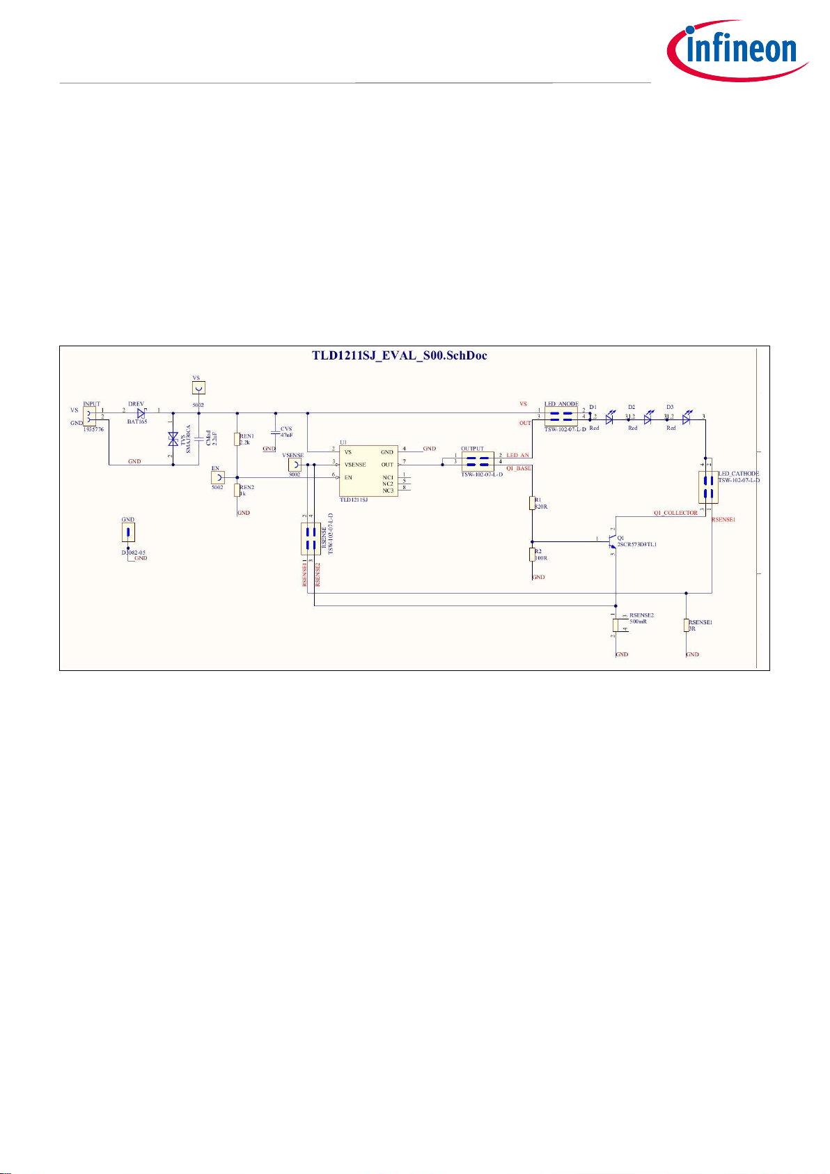
3 Schematics, layout and bill of material
For the calculation of the external components required for the LITIX™ Linear TLD1211SJ and used on the
TLD1211SJ_EVAL board refer to the following documentation:
• LITIX™ Linear TLD1211SJ datasheet
• LED driving concepts and Linear LED drivers
3.1 Schematics
The schematic of the TLD1211SJ_EVAL board is shown in Figure 6.
Figure 6 Schematic of TLD1211SJ_EVAL board
Page 8

User Manual Please read the Important Notice and Warnings at the end of this document V 1.0
www.infineon.com page 8 of 11 2021-01-13
TLD1211SJ evaluation board
User Manual
Schematics, layout and bill of material
3.2 Layout
Figure 7 and Figure 8 show the layout of the TLD1211SJ_EVAL board.
Figure 7 Layout of TLD1211SJ_EVAL board – top layer
Figure 8 Layout of TLD1211SJ_EVAL board – bottom layer
Page 9

User Manual Please read the Important Notice and Warnings at the end of this document V 1.0
www.infineon.com page 9 of 11 2021-01-13
TLD1211SJ evaluation board
User Manual
Schematics, layout and bill of material
3.3 Bill of materials
Table 4 shows theTLD1211SJ_EVAL board bill of material.
Table 4 Bill of material
Designator
Value
Manufacturer
Manufacturer order number
CMod
2.2 µF
MuRata
GRM31CR71H225KA88
CVS
47 nF
TDK Corporation
CGA3E2X8R1H473K080AA
D1, D2, D3
Red
OSRAM Opto
Semiconductors
LR H9PP-HZJZ-1-1
DREV
BAT165
Infineon Technologies AG
BAT165
EN, VS, VSENSE
5002
Keystone Electronics Corp.
5002
GND
D3082-05
Harwin
D3082-05
INPUT
1935776
Phoenix Contact
1935776
LED_ANODE,
LED_CATHODE, OUTPUT,
RSENSE
TSW-102-07-L-D
Samtec
TSW-102-07-L-D
Q1
2SCR573D3TL1
ROHM Semiconductors
2SCR573D3TL1
R1
820 Ω
Yageo
RC0603FR-07820RL
R2
100 Ω
Yageo
RC0603FR-07100RL
REN1
2.2 kΩ
Yageo
RC0603FR-072K2L
REN2
1 kΩ
Yageo
RC0603FR-071KL
RSENSE1
3 Ω
Panasonic
ERJ-1TRQF3R0V
RSENSE2
500 mΩ
Vishay
WSL2512R5000DEA
TVS
SMAJ30CA
Littelfuse
SMAJ30CA
U1
TLD1211SJ
Infineon Technologies AG
TLD1211SJ
3.4 PCB design data
The Altium project is available on the TLD1211SJ_EVAL website.
Page 10

User Manual Please read the Important Notice and Warnings at the end of this document V 1.0
www.infineon.com page 10 of 11 2021-01-13
TLD1211SJ evaluation board
User Manual
Revision history
Revision history
Document
version
Date of release
Description of changes
V 1.0
2021-01-13
Initial release
Page 11

Trademarks
All referenced product or service names and trademarks are the property of their respective owners.
Edition 2021-01-13
Z8F80042284
Published by
Infineon Technologies AG
81726 Munich, Germany
© 2021 Infineon Technologies AG.
All Rights Reserved.
Do you have a question about this
document?
Email: erratum@infineon.com
Document reference
IMPORTANT NOTICE
The information contained in this application note is
given as a hint for the implementation of the product
only and shall in no event be regarded as a
description or warranty of a certain functionality,
condition or quality of the product. Before
implementation of the product, the recipient of this
application note must verify any function and other
technical information given herein in the real
application. Infineon Technologies hereby disclaims
any and all warranties and liabilities of any kind
(including without limitation warranties of noninfringement of intellectual property rights of any
third party) with respect to any and all information
given in this application note.
The data contained in this document is exclusively
intended for technically trained staff. It is the
responsibility of customer’s technical departments
to evaluate the suitability of the product for the
intended application and the completeness of the
product information given in this document with
respect to such application.
For further information on the product, technology,
delivery terms and conditions and prices please
contact your nearest Infineon Technologies office
(www.infineon.com).
WARNINGS
Due to technical requirements products may contain
dangerous substances. For information on the types
in question please contact your nearest Infineon
Technologies office.
Except as otherwise explicitly approved by Infineon
Technologies in a written document signed by
authorized representatives of Infineon
Technologies, Infineon Technologies’ products may
not be used in any applications where a failure of the
product or any consequences of the use thereof can
reasonably be expected to result in personal injury.
 Loading...