

Page 1
Data Sheet, V 1.1, November 2005
TDK5100F
434 MHz ASK/FSK Transmitter in 10-pin
Package
Wireless Control
Components
Never stop thinking.
Page 2

Edition 2005-11-14
Published by In fineon Technologies AG,
St.-Martin-Strasse 53,
81669 München, Germany
© Infineon Technologies AG 2005-11-14.
All Rights Reserved.
Attention please!
The information herein is given to describe certain components and shall not be considered as a guarantee of
characteristics.
Terms of delivery and rights to technical change reserved.
We hereby disclaim any and all warranties, including but not limited to warranties of non-infringement, regarding
circuits, descriptions and charts stated herein.
Information
For further information on tech nology, delivery terms and conditions and prices please contact your nearest
Infineon Technologies Office in Germany or the Infineon Technologies Companies and our Infineon Technologies
Representatives worldwide (www.infineon.com).
Warnings
Due to technical requirements components may contain dangerous substances. For information on the types in
question please contact your nearest Infineon Technologies Office.
Infineon Technologies Components may only be used in life-support devices or systems with the express written
approval of Infineon T echnologies, if a failure of such components can reasonably be expected to cause the failure
of that life-support device or system, or to affect the safety or effectiveness of that device or system. Life support
devices or systems are intended to be implanted in the human body, or to support and/or maintain and sustain
and/or protect human life. If they fail, it is reasonable to assume that the health of the user or other persons may
be endangered.
Page 3

Data Sheet, V 1.1, November 2005
TDK5100F
434 MHz ASK/FSK Transmitter in 10-pin
Package
Wireless Control
Components
Never stop thinking.
Page 4
TDK5100F
Revision History: 2005-11-14 V 1.1
Previous Version: none
Page Subjects (major changes since last revision)
We Listen to Your Comments
Any information within this document that you feel is wrong, unclear or missing at all?
Your feedback will help us to continuously improve the quality of this document.
Please send your proposal (including a reference to this document) to:
petra.haidn@infineon.com
Page 5

TDK5100F
Table of Contents Page
1 Product Description . . . . . . . . . . . . . . . . . . . . . . . . . . . . . . . . . . . . . . . . . 6
1.1 Overview . . . . . . . . . . . . . . . . . . . . . . . . . . . . . . . . . . . . . . . . . . . . . . . . . . . 6
1.2 Features . . . . . . . . . . . . . . . . . . . . . . . . . . . . . . . . . . . . . . . . . . . . . . . . . . . . 6
1.3 Application . . . . . . . . . . . . . . . . . . . . . . . . . . . . . . . . . . . . . . . . . . . . . . . . . . 6
2 Functional Description . . . . . . . . . . . . . . . . . . . . . . . . . . . . . . . . . . . . . . . 7
2.1 Pin Configuration . . . . . . . . . . . . . . . . . . . . . . . . . . . . . . . . . . . . . . . . . . . . . 7
2.2 Pin Definition and Functions . . . . . . . . . . . . . . . . . . . . . . . . . . . . . . . . . . . . 7
2.3 Functional Block Diagram . . . . . . . . . . . . . . . . . . . . . . . . . . . . . . . . . . . . . 12
2.4 Functional Block Description . . . . . . . . . . . . . . . . . . . . . . . . . . . . . . . . . . . 13
2.4.1 PLL Synthesizer . . . . . . . . . . . . . . . . . . . . . . . . . . . . . . . . . . . . . . . . . . . 13
2.4.2 Crystal Oscillator . . . . . . . . . . . . . . . . . . . . . . . . . . . . . . . . . . . . . . . . . . 13
2.4.3 Power Amplifier . . . . . . . . . . . . . . . . . . . . . . . . . . . . . . . . . . . . . . . . . . . 13
2.4.4 Power Modes . . . . . . . . . . . . . . . . . . . . . . . . . . . . . . . . . . . . . . . . . . . . . 14
2.4.4.1 Power Down Mode . . . . . . . . . . . . . . . . . . . . . . . . . . . . . . . . . . . . . . 14
2.4.4.2 PLL Enable Mode . . . . . . . . . . . . . . . . . . . . . . . . . . . . . . . . . . . . . . . 14
2.4.4.3 Transmit Mode . . . . . . . . . . . . . . . . . . . . . . . . . . . . . . . . . . . . . . . . . . 15
2.4.4.4 Power mode control . . . . . . . . . . . . . . . . . . . . . . . . . . . . . . . . . . . . . . 15
2.4.5 Recommended Timing Diagrams for ASK- and FSK-Modulation . . . . . 16
3 Applications . . . . . . . . . . . . . . . . . . . . . . . . . . . . . . . . . . . . . . . . . . . . . . . 19
3.1 50 Ohm-Output Testboard Schematic . . . . . . . . . . . . . . . . . . . . . . . . . . . . 19
3.2 50 Ohm-Output Testboard Layout . . . . . . . . . . . . . . . . . . . . . . . . . . . . . . . 20
3.3 Bill of Material (50 Ohm-Output Evalboard) . . . . . . . . . . . . . . . . . . . . . . . . 21
3.4 Stripline-Antenna Testboard Schematic . . . . . . . . . . . . . . . . . . . . . . . . . . 22
3.5 Stripline-Antenna Testboard Layout . . . . . . . . . . . . . . . . . . . . . . . . . . . . . 23
3.6 Bill of Material (Antenna board) FSK modulation . . . . . . . . . . . . . . . . . . . . 24
3.7 Application Hints on the Crystal Oscillator . . . . . . . . . . . . . . . . . . . . . . . . . 25
3.8 Design Hints on the Clock Output (CLKOUT) . . . . . . . . . . . . . . . . . . . . . . 27
3.9 Application Hints on the Power-Amplifier . . . . . . . . . . . . . . . . . . . . . . . . . . 28
4 Reference . . . . . . . . . . . . . . . . . . . . . . . . . . . . . . . . . . . . . . . . . . . . . . . . . 30
4.1 Electrical Data . . . . . . . . . . . . . . . . . . . . . . . . . . . . . . . . . . . . . . . . . . . . . . 30
4.1.1 Absolute Maximum Ratings . . . . . . . . . . . . . . . . . . . . . . . . . . . . . . . . . . 30
4.2 Operating Ratings . . . . . . . . . . . . . . . . . . . . . . . . . . . . . . . . . . . . . . . . . . . 31
4.3 AC/DC Characteristics . . . . . . . . . . . . . . . . . . . . . . . . . . . . . . . . . . . . . . . . 31
4.3.1 AC/DC Characteristic at 3V, 25°C . . . . . . . . . . . . . . . . . . . . . . . . . . . . . 31
4.3.2 AC/DC Characteristic at 2.1V ...4.0 V, -40°C ...+125°C . . . . . . . . . . . . 33
5 Package Outlines . . . . . . . . . . . . . . . . . . . . . . . . . . . . . . . . . . . . . . . . . . . 36
Data Sheet 5 V 1.1, 2005-11-14
Page 6

TDK5100F
Product Description
1 Product Description
1.1 Overview
The TDK 5100 F is a single chip ASK/F SK transmitter for ope ration in the frequ ency band
433-435 MHz. The IC offers a high level of integration and needs only a few external
components. The device conta ins a fully integr ated PLL synthes izer and a hig h efficiency
power amplifier to drive a loop antenna. A special circuit design and an unique power
amplifier design are use d to save curre nt consump tion and there fore to save ba ttery life.
Additional features are a power down mode and a divided clock output.
1.2 Features
• fully integrated frequency synthesizer
• VCO without external components
• ASK and FSK modulation
• frequency range 433-435 MHz
• high efficiency power amplifier (typically 5 dBm)
• low supply current
• voltage supply range 2.1 ... 4 V
• temperature range −40 ... +125°C
• power down mode
• crystal oscillator 13.56 MHz
• FSK-switch
• divided clock output for µC
• low external component count
1.3 Application
• Tire pressure monitoring systems
• Keyless entry systems
• Remote control systems
• Alarm syst ems
• Communication systems
Data Sheet 6 V 1.1, 2005-11-14
Page 7
2 Functional Description
2.1 Pin Configurat ion
TDK5100F
Functional Description
CLKOUT
VS
GND
FSKOUT
COSC
1
2
3
4
5
TDK 5100F
10
9
8
7
6
PDWN
PAOUT
PAGND
FSKDTA
ASKDTA
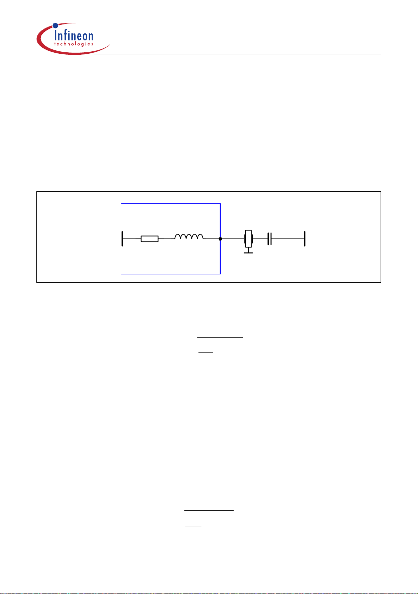
Figure 1 IC Pin Configuration
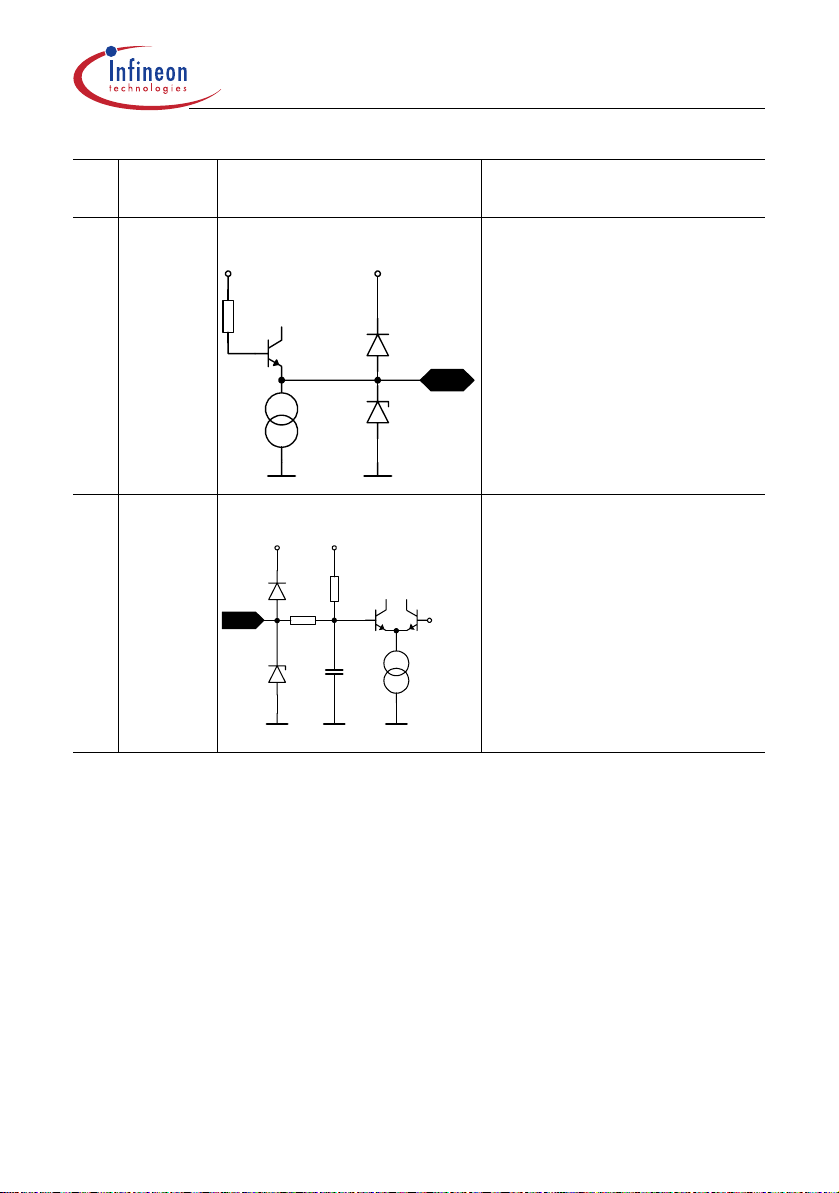
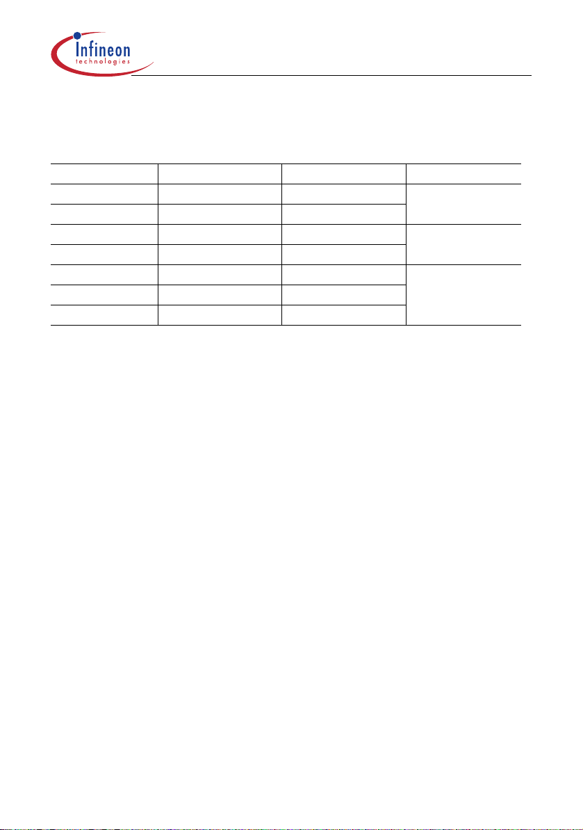
2.2 Pin Definition and Functions
Table 1 Pin Definition and Functions - Overview
Pin
No.
1 CLKOUT Clock Driver Output (847.5 kHz)
2 VS Voltage Supply
3 GND Ground
4 FSKOUT Frequency Shift Keying Switch Output
5 COSC Crystal Oscillator Input (13.56 MHz)
6 ASKDTA Amplitude Shift Keying Data Input
7 FSKDTA Frequency Shift Keying Data Input
8 PAGND Power Amplifier Ground
9 PAOUT Power Amplifier Output (434 MHz)
10 PDWN Power Down Mode Control
Symbol Function
Data Sheet 7 V 1.1, 2005-11-14
Page 8
TDK5100F
Functional Description
Table 2 Pin Definition and Function
Pin
Symbol Interface Schematic Function
1)
No.
1 CLKOUT Clock output to supply an external
V
S
1
device.
An external pull-up resisto r has to
be added in accordance to the
driving requirements of the
300 Ω
external device.
The clock frequenc y is 847.5 kHz .
2 VS This pin is the positive supply of
the transmitter electronics.
An RF bypass capaci tor should be
connected directly to this pin and
returned to GND (pin 3) as short
as possible.
3 GND General ground connecti on.
4 FSKOUT This pin is connec ted to a switch to
V
S
V
S
GND (pin 3).
The switch is closed when the
signal at FSKDTA (pin 7) is in a
200 µA
logic low state.
4
The switch is open w hen the signal
at FSKDTA (pin 7) is in a l ogic high
120 kΩ 200 kΩ
state.
FSKOUT can switch an ad dition al
capacitor to the reference crystal
network to pull the crystal
frequency by an amount resulting
in the desired FSK freque ncy s hift
of the transmitter output
frequency.
Data Sheet 8 V 1.1, 2005-11-14
Page 9
TDK5100F
Functional Description
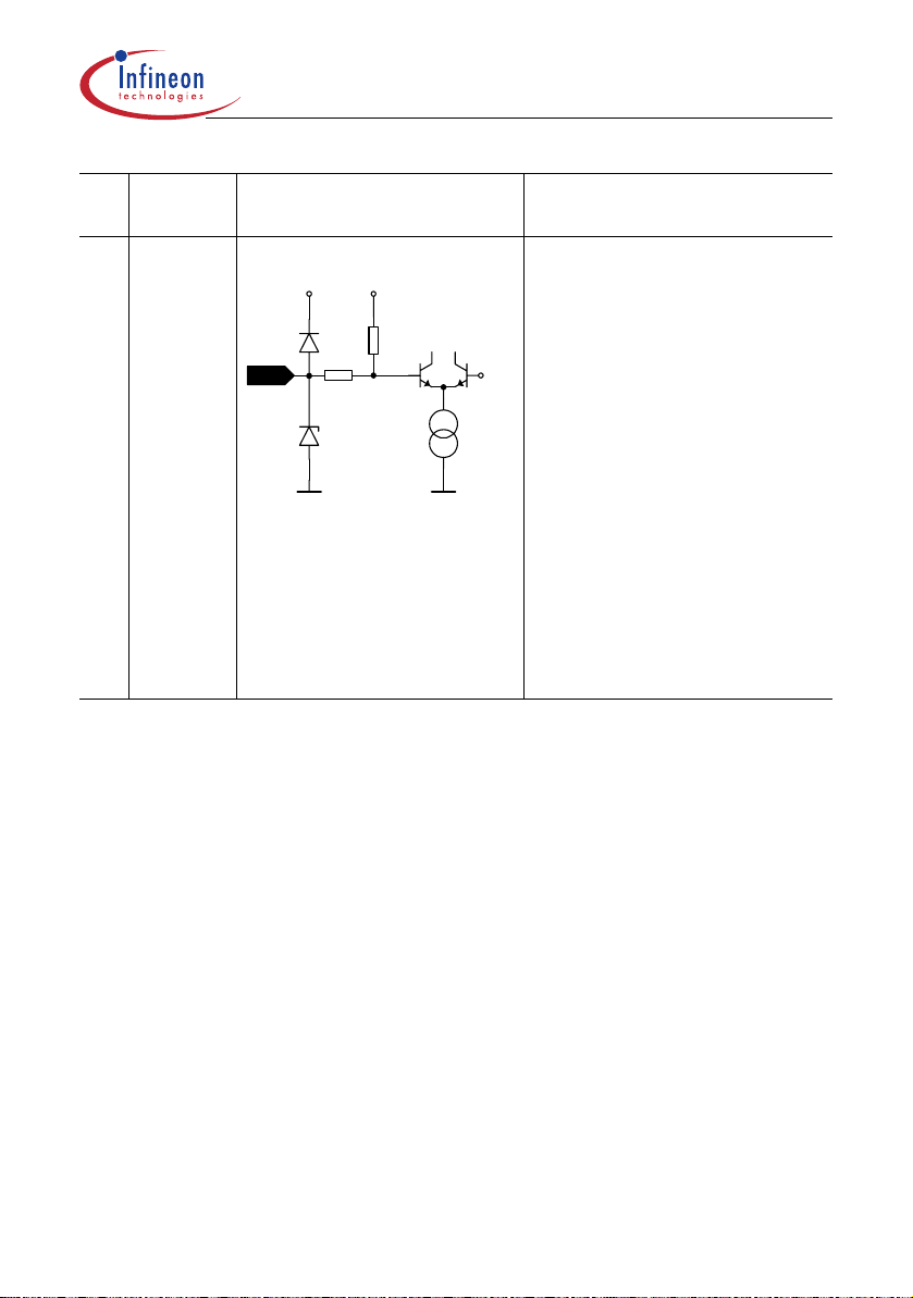
Pin
Symbol Interface Schematic Function
No.
5 COSC This pin is connected to the
V
S
6 kΩ
100 µA
V
S
6 ASKDTA Digital amplitude modulation can
+1.2 V
V
S
60 k
6
90 k
Ω
Ω
50 pF 30 µA
reference oscillator circuit.
The reference oscillat or is working
as a negative impedance
converter. It presents a negative
resistance in series to an
5
inductance at the COSC pin.
be imparted to the Power Amplifier
through this pin.
A logic high (ASKDTA > 1.5 V or
+1.1 V
open) enables the Power
Amplifier.
A logic low (ASKDTA < 0.5 V)
disables the Power Amplifier.
Data Sheet 9 V 1.1, 2005-11-14
Page 10
TDK5100F
V
Functional Description
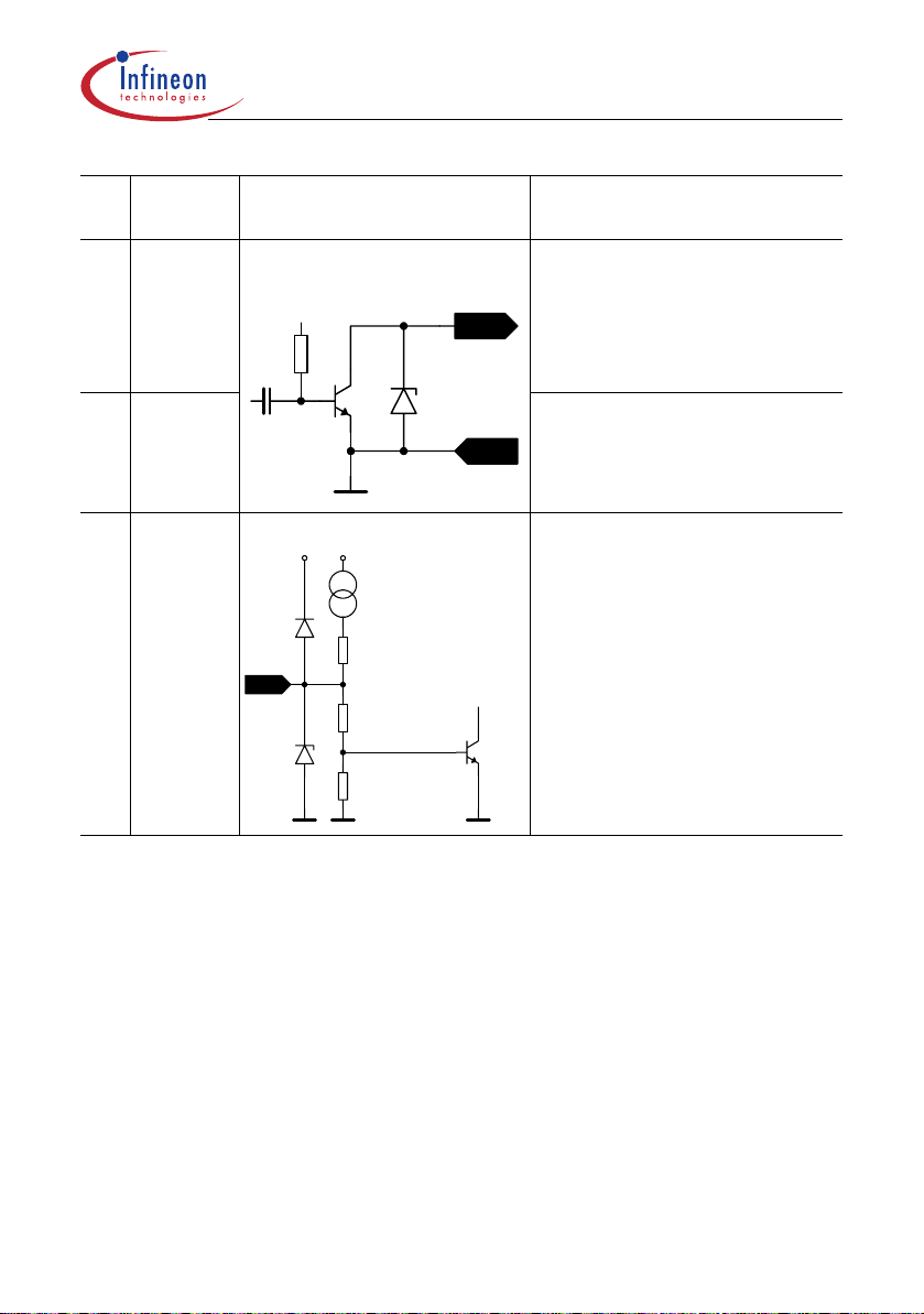
Pin
Symbol Interface Schematic Function
No.
7 FSKDTA Digital frequency modulation can
+1.2 V
V
S
Ω
90 k
60 k
Ω
30 µA
7
be imparted to the Xtal Oscillator
by this pin. The VCO-frequency
varies in accordance to the
frequency of the reference
oscillator.
+1.1
A logic high (FSKDTA > 1.5V or
open) sets the FSK switch to a
high impedance state.
A logic low (FSKDTA < 0.5 V)
closes the FSK switch from
FSKOUT (pin 4) to GND (pin 3).
A capacitor can be s witched to the
reference crystal network this way.
The Xtal Oscillator frequency will
be shifted giving the desi gned FSK
frequency deviation.
Data Sheet 10 V 1.1, 2005-11-14
Page 11
TDK5100F
)
Functional Description
Pin
Symbol Interface Schematic Function
No.
8 PAGND Ground connection of the power
amplifier.
9
The RF ground return path of the
power amplifier output PAOUT
(pin 9) has to be concentrated to
this pin.
9 PAOUT RF output pin of the transmitter.
10 PDWN Disable pin for the complete
V
S
40 µA ∗ (ASKDTA+FSKDTA
10
5 kΩ
150 kΩ
250 kΩ
"ON"
8
A DC path to the positive supply
VS has to be supplied by the
antenna matching network.
transmitter circuit.
A logic low (PDWN < 0.7 V) turns
off all transmitter functions.
A logic high (PDWN > 1.5 V) gi ves
access to all transmitter functions.
PDWN input will be pulled up by
40 µA internally by either setting
FSKDTA or ASKDTA to a logic
high-state.
1) Indicated voltages and currents apply for PLL Enable Mode and Transmit Mode.
In Power Down Mode, the values are zero or high-ohmic.
Data Sheet 11 V 1.1, 2005-11-14
Page 12
2.3 Functional Block Diagram
TDK5100F
Functional Description
Power
Power
ASK
FSK
VS
Supply
Down
Control
Data
Input
Data
Input
Power
9
Power
Output
Amplifier
Ground
Amplifier
8
On
AMP
Power
3
Power
Supply
LF
Ground
10 2
OR
6
7
PFD :64 VCO :2
1
:16
Clock
Output
Osc
XTAL
4
FSK
Switch
5
Crystal
13.56 MHz
Figure 2 Functional Block Diagram
Data Sheet 12 V 1.1, 2005-11-14
Page 13

TDK5100F
Functional Description
2.4 Functional Block Description
2.4.1 PLL Synthesizer
The Phase Locked Loop synthesizer consists of a Voltage Controlled Oscillator (VCO),
an asynchronous divider chain, a phase detector, a charge pump and a loop filter. It is
fully implemented on chip. The tuning circuit of the VCO consisting of spiral inductors
and varactor diodes is on chip, too. Therefore no additional external components are
necessary. The nominal center frequency of the VCO is 868 MHz. The oscillator signal
is fed both, to the synthesizer divider chain and to the power amplifier. The overall
division ratio of the asynchronous divider chain is 64. The phase detector is a Type IV
PD with charge pump. The passive loop filter is realized on chip.
2.4.2 Crystal Oscillator
The crystal oscillator operates at 13.56 MHz.
The crystal frequency is div ided by 16. The resulting 847.5 kHz are avail able at the clock
output CLKOUT (pin1) to drive the clock input of a micro controller.
To achieve FSK transm ission, the oscillator frequency c an be detune d by a fixed am ount
by switching an external capacitor via FSKOUT (pin 4).
The condition of the switch is controlled by the signal at FSKDTA (pin 7).
Table 3 FSKDTA - FSK Switch
FSKDTA (pin7) FSK Switch
1)
Low
Open
2)
, High
3)
CLOSED
OPEN
1) Low: Voltage at pin < 0.5V
2) Open: Pin open
3) High: Voltage at pin > 1.5V
2.4.3 Power Amplifier
The VCO frequency is divided by 2 and fed to the Power Amplifier.
The Power Amplifier can be switched on and off
by the signal at ASKDTA (pin 6).
Data Sheet 13 V 1.1, 2005-11-14
Page 14

TDK5100F
Functional Description
Table 4 ASKDTA - Power Amplifier
ASKDTA (pin6) Power Amplifier
1)
Low
2)
, High
3)
Open
1) Low: Voltage at pin < 0.5V
2) Open: Pin open
3) High: Voltage at pin > 1.5V
The Power Amplifier has an Open Collector output at PAOUT (pin 9) and requires an
external pull-up coil to provide bias. The coil is part of the tuning and matching LC
circuitry to get best performance with the external loop antenna. To achieve the best
power amplifier effici ency, the hig h frequency voltage swi ng at PAOUT (pin 9) sho uld be
twice the supply voltage.
The power amplifier has its own ground pin PAGND (pin 8) in order to reduc e the amount
of coupling to the other circuits.
OFF
ON
2.4.4 Power Modes
The IC prov ides three power mo des, the POWER DOWN M ODE, the PLL ENABLE
MODE and the TRANSMIT MODE.
2.4.4.1 Power Down Mode
In the POWER DOWN MODE the complete chip is switched off.
The current consumption is typically 0.3 nA at 3 V 25°C.
This current doubles every 8°C. The values for higher temperatures are
typically 14 nA at 85°C and typically 600 nA at 125°C.
2.4.4.2 PLL Enable Mode
In the PLL ENABLE MODE the PLL is switched on but the power amplifier is turned off
to avoid unde s ir ed po we r r a di at i o n dur in g th e t im e t he PLL n ee ds to set t l e. The tu rn on
time of the PLL is determined mainly by the turn on time of the crystal oscillator and is
less than 1 msec when the specified crystal is used.
The current consumption is typically 3.5 mA.
Data Sheet 14 V 1.1, 2005-11-14
Page 15

TDK5100F
Functional Description
2.4.4.3 Transmit Mode
In the TRANSMIT MODE th e PLL is switched on and t he power amplifier is turne d on too.
The current consumption of the IC is typically 7 mA when using a proper transforming
network at PAOUT, see Figure 8.
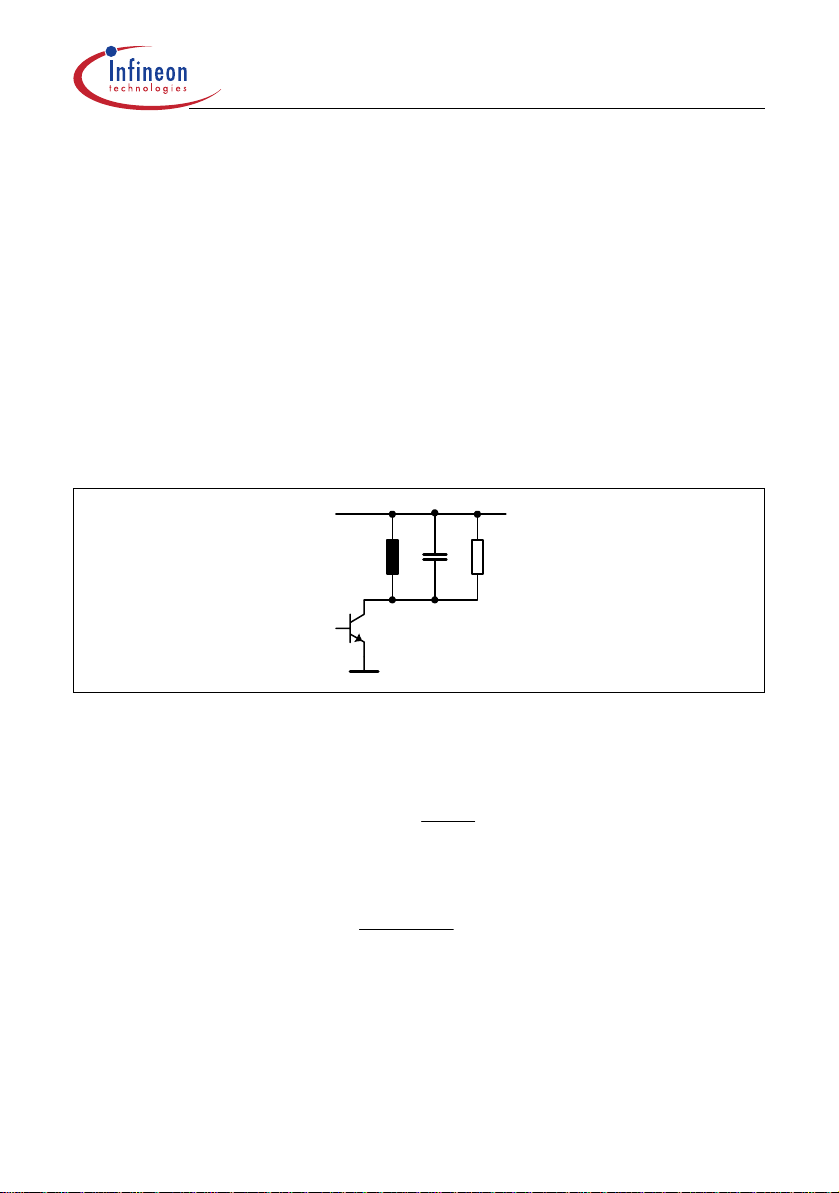
2.4.4.4 Power mode control
The bias circuitry is powered up via a voltage V > 1.5 V at the pin PDWN (pin10).
When the bias circuitry is powered up, the pins ASKDTA and FSKDTA are pulled up
internally.
Forcing the voltage at the pins low overrides the internally set state.
Alternatively, if the voltage at ASKDTA or FSKDTA is forced high ex terna lly, the PDWN
pin is pulled up inter nally via a cur rent sou rce. In this c ase, it is no t necessary to connect
the PDWN pin, it is recommended to leave it open.
The principle schematic of the power mode control circuitry is shown in Figure3
PDWN
ASKDTA
FSKDTA
On
OR
Bias
Source
120 kΩ
FSKOUT
PAOUT
Bias Voltage
120 kΩ
PLL
434
MHz
PA
On
FSK
IC
Figure 3 Power mode control circuitry
Data Sheet 15 V 1.1, 2005-11-14
Page 16
TDK5100F
Functional Description
Table 5 provides a listing of how to get into the different power modes
Table 5 Power Modes
PDWN FSKDTA ASKDTA MODE
1)
Low
2)
Open
3)
High
Open High Low
High Low, Open, High Open, High TRANSMIT
Open High Open, High
Open Low, Open, High High
1) Low: Voltage at pin < 0.7V (PDWN)
2) Open: Pin open
3) High: Voltage at pin > 1.5V
Other combinations of the control pins PDWN, FSKDTA and ASKDTA are not
recommended.
Low, Open Low, Open POWER DOWN
Low Low
Low, Open, High Low PLL ENABLE
Voltage at pin < 0.5V (FSKDTA, ASKDTA)
Data Sheet 16 V 1.1, 2005-11-14
Page 17
TDK5100F
Functional Description
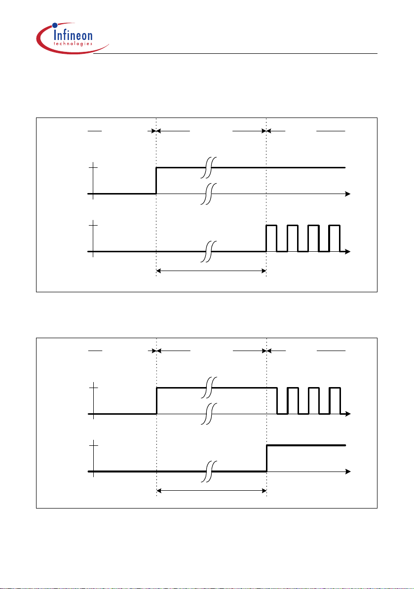
2.4.5 Recommended Timing Diagrams for ASK- and FSK-Modulation
ASK Modulation using FSKDTA and ASKDTA, PDWN not connected
Modes: TransmitPLL EnablePower Down
High
FSKDTA
Low
Open, High
ASKDTA
Low
Figure 4 ASK Modulation
FSK Modulation using FSKDTA and ASKDTA, PDWN not connected.
to
DATA
to
min. 1 msec.
t
t
Modes: TransmitPLL EnablePower Down
DATA
High
FSKDTA
Low
High
to
t
ASKDTA
Low
to
min. 1 msec.
t
Figure 5 FSK Modulation
Data Sheet 17 V 1.1, 2005-11-14
Page 18

Alternative ASK Modulation, FSKDTA not connected.
Modes: TransmitPLL EnablePower Down
High
PDWN
Low
Open, High
to
ASKDTA
Low
to
min. 1 msec.
Figure 6 Alternative ASK Modulation
Alternative FSK Modulation
TDK5100F
Functional Description
t
DATA
t
Modes: TransmitPLL EnablePower Down
High
PDWN
Low
Open, High
to
t
ASKDTA
Low
Open, High
to
DATA
t
FSKDTA
Low
to
t
min. 1 msec.
Figure 7 Alternative FSK Modulation
Data Sheet 18 V 1.1, 2005-11-14
Page 19
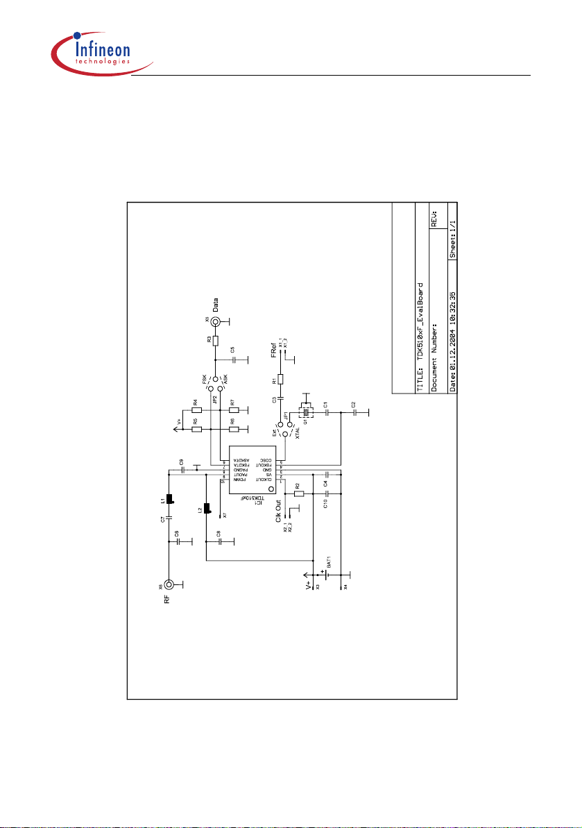
3 Applications
3.1 50 Ohm-Output Testboard Schematic
TDK5100F
Applications
Figure 8 50 Ohm-output testboard schematic
Data Sheet 19 V 1.1, 2005-11-14
Page 20

3.2 50 Ohm-Output Testboard Layout
Figure 9 Top Side of TDK5100 F-Testboard with 50 Ohm-Output
TDK5100F
Applications
Figure 10 Bottom Side of TDK5100 F-Testboard with 50 Ohm-Output
Data Sheet 20 V 1.1, 2005-11-14
Page 21
TDK5100F
Applications
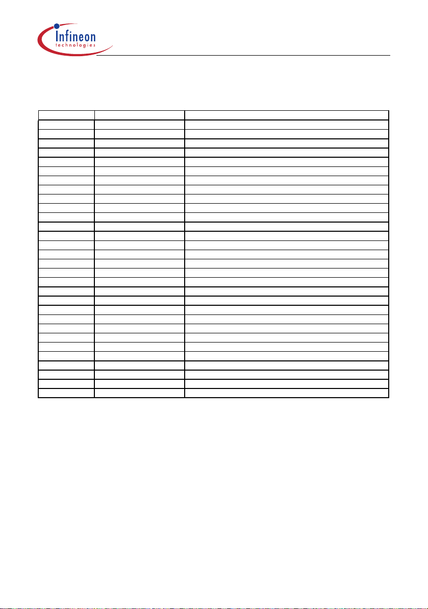
3.3 Bill of Material (50 Ohm-Output Evalboard)
Reference Value Specification
R1 open
R2 open
R3 4k 7 0603, +/-5%
R4 12k 0603, + /-5%
R5 open
R6 15k 0603, + /-5%
R7 open
C1 10p 0603, C0G, + /-1%
C2 6p8 0603, C0G, + /-0,1p
C3 open
C4 open
C5 100p 0603, X7R, +/-10%
C6 12p 0603, C0G, + /-1%
C7 39p 0603, C0G, + /-1%
C8 330p 0603, C0G, + /-5%
C9 3p3 0603, C0G, + /-0,1p
C10 47n 0603, X7R, +/-10%
L1 47n EPCOS S IMID 0603-C, +/-2%
L2 120n EPCOS S IMID 0603-C, +/-2%
X1 n.e.
X2 n.e.
X3 Pin single-pole connector, 2,54m m
X4 Pin single-pole connector, 2,54m m
X5 SMA-connec tor
X6 SMA-connec tor
X7 n.e.
JP1 solder bridge in position "XTAL"
JP2 solder bridge in position "F SK"
Q1 13,56875 MHz , Tokyo Denpa TSS-3B 13,56875 M Hz S pec .No. 10-50205
IC1 TDK5100F
Data Sheet 21 V 1.1, 2005-11-14
Page 22

3.4 Stripline-Antenna Testboard Schematic
TDK5100F
Applications
Figure 11 Stripline-antenna testboard schematic
Data Sheet 22 V 1.1, 2005-11-14
Page 23

TDK5100F
Applications
3.5 Stripline-Antenna Testboard Layout
Figure 12 Top Side of TDK5100 F-Testboard with Stripline-Antenna
Figure 13 Bottom Side of TDK5100 F-Testboard with Stripline-Antenna
Please note that this board layout may be used for both high- and low-power
applications, see also the bill of materials on the subsequent pages.
In case of ASK operation the solder bridge JP2 has to be shortened in the “ASK”position, in case of FSK modulation in the“FSK” position.
Solder bridge JP1between C1, C2 and C3) gives a choice of operating the board with
the on-board crystal as refe rence (“XT AL” shorte ned, i.e . close to C1 and C2) or with an
external clock generator (solder bridge shorts pads between C3 and C2).
Data Sheet 23 V 1.1, 2005-11-14
Page 24

3.6 Bill of Material (Antenna board) FSK modulation
Reference
Value
Specification
13,56875 MHz,
Tokyo Denpa TSS-3B 13,56875 MHz Spec.No. 10-
R1 open
R2 0R 0603, SMD-Jumper
R3 0R 0603, SMD-Jumper
R4 82k 0603, +/-5%
R5 open
R6 open
R7 100n 0603, X7R, +/-10%
R8 39R 0603, +/-1%
R9 15k 0603, +/-5%
C1 10p 0603, C0G, +/-1%
C2 6p8 0603, C0G, +/-0,1p
C3 open
C4 open
C5 open
C6 10n 0603, X7R, +/-10%
C7 5p6 0603, C0G, +/-0,1p
C8 open
C9 4p7 0603, C0G, +/-0,1p
C10 47n 0603, X7R, +/-10%
L1 100n 0603, EPCOS SIMID, +/-2%
L2 0R 0603, SMD-Jumper
X1 n.e.
X3 n.e.
X4 n.e.
S1 push-button STTSKHMPW, ALPS
JP1 solder bridge in position "XTAL"
JP2 solder bridge in position "FSK"
Q1
IC1 TDK5100F P-TSSOP-10
IC2 HCS360 SO8
BAT1 battery holder HU2031-1, Renata
battery CR2032, Renata
TDK5100F
Applications
Data Sheet 24 V 1.1, 2005-11-14
Page 25
TDK5100F
L
CL
C
1
C
Applications
3.7 Application Hints on the Crystal Oscillator
Application Hints on the crystal oscillator
The crystal oscilla tor achieves a turn on time le ss than 1 msec wh en the specifi ed crystal
is used. To achieve this, a NIC oscillator type is implemented in the TDK 5100 F. The
input impedance of this oscillator is a negative resistance in series to an inductance.
Therefore the load capacitance of the crystal CL (specified by the crystal supplier) is
transformed to the capacitance Cv.
-R L f, CL Cv
IC
Figure 14 Application Hints
Formula 1:
1
=
v
1
2
ω
+
CL: crystal load capacitance for nominal frequency
ω: angular frequency
L: inductance of the crystal oscillator
Example for the ASK-Mode:
Referring to the application circuit, in ASK-Mode the capacitance C2 is replaced by a
short to ground. Assume a crys tal frequency of 13.56M Hz and a crystal load ca pacitance
of CL = 12 pF. The inducta nce L at 13.56MHz is about 4.6 µH. Therefore C1 is calculated
to 10 pF.
v =
=
1
1
+
ω
C
2
L
CL
Data Sheet 25 V 1.1, 2005-11-14
Page 26

TDK5100F
)
C
Applications
Example for the FSK-Mode:
FSK modulation is achieved by switching the load capacitance of the crystal as shown
below.
FSKDTA
FSKOUT
Csw
-R L f, CL Cv1
IC
Figure 15 FSK Mode
The frequency deviation of the crystal oscillator is multiplied with the divider factor N of
the Phase Locked Loop to the output of the power amplifier. In case of small frequency
deviations (up to +/- 1000 ppm), the two desired load capacitances can be calculated
with the formula below.
L
=±
1
CL: crystal load capacitance for nominal frequency
C0: shunt capacitance of the crystal
f: frequency
ω: ω = 2
N: division ratio of the PLL
df: peak frequency devia tio n
πf: angular frequency
COSC
f
∆
CCL
0
m
∆
±
1(
+
fN
1*
f
1(
+
fN
1*
CLC
+
C
1
CLC
)0(2
+
)
C
1
Cv2
)0(2
Because of the inductive part of the TDK 5100 F, these values must be corrected by
Formula 1 on the preceding page. The value of Cv± can be calculated.
Data Sheet 26 V 1.1, 2005-11-14
Page 27

TDK5100F
L
C
)
C
D
Applications
CL
1
1
2
ω
+
±
1()(1
CswCvCvCvCsw
+∗+−∗
1)(
CvCv
−+
v
=±
If the FSK switch is clos ed, Cv- is equal to Cv1 (C1 in the application diagram). If the
FSK switch is open, Cv2 (C2 in the application diagram) can be calculated.
22
C
v
Csw: parallel capacitance of the FSK switch (3 pF incl. layout parasitics)
Remark: These calculations are only approximations. The necessary values depend
on the layout also and must be adapted for the specific application board.
==
3.8 Design Hints on the Clock Output (CLKOUT)
The CLKOUT pin is an o pen co llecto r output . An exte rnal pu ll up re sisto r (RL) shou ld be
connected between this pin and the positive supply voltage. The value of RL is
depending on the clock freque ncy and the load capacit ance CLD (PCB board plu s input
capacitance of the microcontroller). RL can be calculated to:
=
fCLKOUTRL*8*
1
CL
Table 6 Clock Output
fCLKOUT=847.5 kHz
CL[pF] RL[kOhm]
527
10 12
20 6.8
Remark: To achieve a low current consumption and a low
spurious radiation, the largest possible RL should be chosen.
Data Sheet 27 V 1.1, 2005-11-14
Page 28
TDK5100F
S
00316
.0*
2
Applications
Even harmonics of the signal at CLKOUT can interact with the crystal oscillator input
COSC preventing the start-up of oscillation. Care must be taken in layout by sufficient
separation of the signal lines to ensure sufficiently small coupling.
3.9 Application Hints on the Power-Amplifier
The power amplifier operates in a high efficient class C mode. This mode is
characterized by a pulsed operation of the power amplifier transistor at a current flow
angle of θ<<π. A frequency selective network at the amplifier output passes the
fundamental frequency component of the pulse spectrum of the collector current to the
load. The load and its resonance transformation to the collector of the power amplifier
can be generalized by the equivalent circuit of Figure 16. The tank circuit L//C//RL in
parallel to the output impedance of the transistor should be in resonance at the
operating frequency of the transmitter.
V
CL
R
L
Figure 16 Equivalent power amplifier tank circuit
The optimum load at the collector of the power amplifier for “critical” operation under
idealized conditions at resonance is:
2
V
S
=
R
LC
P
*2
O
The theoretical value of RLC for an RF output power of Po= 5 dBm (3.16 mW) is:
2
R
LC
3
Ω== 1423
“Critical” operation is characterized by the RF peak voltage swing at the collector of the
PA transistor to just reach the supply voltage V
.
S
The high degree of efficiency under “critical” operating conditions can be explained by
the low power losses at the transistor. During the conducting phase of the transistor, its
collector voltage is very small. This way the power loss of the transistor, equal to i
C*uCE
is minimized. This is particularly true for small current f low angles of θ<<π.
Data Sheet 28 V 1.1, 2005-11-14
Page 29

TDK5100F
P
S
T
Applications
In practice the R F-sat uration vol tage o f the PA transi stor and o ther p arasiti cs redu ce the
“critical” R
The output power Po is reduced by op era t ing in an “ove r cri t ic al ” mo de ch ara ct e ris ed by
> RLC.
R
L
The power efficiency (and the bandwidth) increase when operating at a slightly higher
, as shown in Figure 17.
R
L
The collector efficiency E is defined as
The diagram of Figure 17 was m easure d direct ly at the PA-ou tput at VS = 3 V. Losses i n
the matching circuitry decr eas e the outp ut po we r by ab out 1.5 dB. As can be se en fro m
the diagram, 550 Ω is the optimu m impedance fo r operation at 3 V. For an approximation
of R
OPT
and
LC
and P
.
O
E
=
IV
CS
at other supply voltages those two formulas can be used:
OUT
VR ~
OPT
RP ~
OUT
OP
10*E
Po [m W ]
7
6
5
4
3
2
1
0
0 1000 2000 3000
Figure 17 Output power P
(mW) and collector efficiency E vs. load resistor RL.
o
10*E
Po
RL [Ohm ]
The DC collector current Ic of the power amplifier and the RF output power Po vary with
the load resistor R
. This is typical for overcritical operation of class C amplifiers. The
L
collector current will sho w a charac teristic dip at the resonanc e frequenc y for this type of
“overcritical” operation. The depth of this dip will increase with higher values of RL.
Data Sheet 29 V 1.1, 2005-11-14
Page 30

TDK5100F
Reference
4 Reference
4.1 Electrical Data
4.1.1 Absolute Maximum Ratings
Attention: The maximum ratings must not be ex ceeded under any circumstances,
not even momentarily and individually, as permanent dam age to th e IC
will result.
Table 7 Absolute Maximum Ratings, T
= -40 °C … +125 °C
amb
Parameter Symbol Limit Values Unit Remarks
min. max.
Junction Temperature T
Storage Temperature T
Thermal Resistance R
Supply voltage V
Voltage at any pin
J
s
thJA
S
V
pins
−40 +150 °C
−40 +125 °C
220 K/W
−0.3 +4.0 V
-0.3 VS + 0.3 V
excluding pin 9
Voltage at pin 9 V
ESD integrity, all pins V
pin9
ESD
-0.3 2 * VS V No ESD-Diode to V
-1 +1 kV JEDEC Standard
JESD22-A114-B
ESD integrity, all pins
excluding pin 9
V
ESD
-2 +2 kV JEDEC Standard
JESD22-A114-B
Ambient Temperature under bias: TA = −40°C to +125°C
Note: All voltages referred to ground (pins) unless stated otherwise.
Pins 3 and 8 are grounded.
S
Data Sheet 30 V 1.1, 2005-11-14
Page 31

TDK5100F
Reference
4.2 Operating Ratings
Within the operational range the IC operates as described in the circuit description.
Table 8 Operating Ratings
Parameter Symbol Limit Values Unit Test Conditions
min. max.
Supply voltage V
Ambient temperature T
S
A
2.1 4.0 V
-40 125 °C
4.3 AC/DC Characteristics
AC/DC characteristics involve the spread of values guaranteed within the specified
supply voltage and ambient temperature. Typical charcateristics are the median of the
production.
4.3.1 AC/DC Characteristic at 3V, 25°C
Table 9 Supply Voltage VS=3V, Ambient temperature T
amb
=25°C
Parameter Symbol Limit Values Unit Test
Conditions
Current consumption
Power Down mode I
S PDWN
min. typ. max.
0.3 100 nA V (Pins 10, 6
and 7)
< 0.2 V
PLL Enable mode I
Transmit mode
S PLL_EN
I
TRANSM
S
3.5 4.2 mA
7mA
434 MHz
Output frequency
Output frequency f
OUT
434 MHz f
OUT
= 32 * f
COSC
Clock Driver Output (Pin 1)
Output current (High) I
Saturation Voltage
1)
(Low)
Data Sheet 31 V 1.1, 2005-11-14
CLKOUT
V
SATL
5µAV
0.56 V I
CLKOUT
CLKOUT
= 1 mA
= V
S
Page 32

TDK5100F
Reference
Table 9 Supply Voltage VS=3V, Ambient temperature T
=25°C (cont’d)
amb
Parameter Symbol Limit Values Unit Test
min. typ. max.
Conditions
FSK Switch Output (Pin 4)
On resistance R
On capacitance C
Off resistance R
Off capacitance C
FSKOUT
FSKOUT
FSKOUT
FSKOUT
10 kΩ V
250 Ω V
6pFV
1.5 pF V
FSKDTA
FSKDTA
FSKDTA
FSKDTA
Crystal Oscillator Input (Pin 5)
Load capacitance C
Serial Resistance of
COSCmax
5pF
100 Ω f = 13.56 MHz
the crystal
Input inductance of the
4.6 µH f = 13.56 MHz
COSC pin
ASK Modulation Data Input (Pin 6)
ASK Transmit disabled V
ASK Transmit enabled V
Input bias current
ASKDTA
ASKDTA
I
ASKDTA
00.5V
1.5 V
S
30 µA V
V
ASKDTA
ASKDTA
Input bias current
I
ASKDTA
-20 µA V
ASKDTA
ASKDTA
ASK data rate f
ASKDTA
20 kHz
FSK Modulation Data Input (Pin 7)
FSK Switch on V
FSK Switch off V
Input bias current
FSKDTA
FSKDTA
I
FSKDTA
00.5V
1.5 V
S
30 µA V
V
FSKDTA
FSKDTA
Input bias current
I
FSKDTA
-20 µA V
FSKDTA
FSKDTA
FSK data rate f
FSKDTA
20 kHz
Power Amplifier Output (Pin 9)
Output Power2) at 434
MHz transformed
to
P
OUT434
5dBm
50 Ohm
= 0 V
= 0 V
= V
S
= V
S
= V
S
= 0 V
= V
S
= 0 V
Data Sheet 32 V 1.1, 2005-11-14
Page 33

TDK5100F
Reference
Table 9 Supply Voltage VS=3V, Ambient temperature T
=25°C (cont’d)
amb
Parameter Symbol Limit Values Unit Test
min. typ. max.
Conditions
Power Down Mode Control (Pin 10)
Power Down mode V
PLL Enable mode V
Transmit mode V
Input bias current
PDWN
PDWN
PDWN
I
PDWN
00.7VV
1.5 V
1.5 V
S
S
VV
VV
30 µA V
ASKDTA
V
FSKDTA
ASKDTA
ASKDTA
PDWN
PDWN
1) Derating linearly to a saturation voltage of max. 140 mV at I
2) Power amplifier in overcritical C-operation
Matching circuitry as used in the 50 Ohm-Output Testboard at the specified frequency.
Tolerances of the pass ive elements not taken into account.
CLKOUT
= 0 mA
4.3.2 AC/DC Characteristic at 2.1V ...4.0 V, -40°C ...+125°C
Table 10 Supply Voltage VS=2.1V ... 4.0V, T
Parameter Symbol Limit Values Unit Test
min. typ. max.
Current consumption
Power Down mode I
PLL Enable mode I
Transmit mode I
S PDWN
S PLL_EN
TRANSM
S
3.5 4.6 mA
7mA
Output frequency
Output frequency
1)
f
OUT
434 MHz f
Clock Driver Output (Pin 1)
Output current (High) I
Saturation Voltage
2)
(Low)
CLKOUT
V
SATL
=-40°C ... +125°C
amb
Conditions
4 µA V (Pins 10, 6
and 7) < 0.2 V
OUT
5µAV
0.5 V I
CLKOUT
CLKOUT
mA
< 0.2 V
< 0.2 V
< 0.5 V
> 1.5 V
= V
= 32 * f
= V
= 0.6
S
COSC
S
Data Sheet 33 V 1.1, 2005-11-14
Page 34

TDK5100F
Reference
Table 10 Supply Voltage VS=2.1V ... 4.0V, T
=-40°C ... +125°C (cont’d)
amb
Parameter Symbol Limit Values Unit Test
min. typ. max.
Conditions
FSK Switch Output (Pin 4)
On resistance R
On capacitance C
Off resistance R
Off capacitance C
FSKOUT
FSKOUT
FSKOUT
FSKOUT
10 kΩ V
280 Ω V
6pFV
1.5 pF V
FSKDTA
FSKDTA
FSKDTA
FSKDTA
Crystal Oscillator Input (Pin 5)
Load capacitance C
Serial Resistance of
COSCmax
5pF
100 Ω f = 13.56 MHz
the crystal
Input inductance of the
4.6 µH f = 13.56 MHz
COSC pin
ASK Modulation Data Input (Pin 6)
ASK Transmit disabled V
ASK Transmit enabled V
Input bias current
ASKDTA
ASKDTA
I
ASKDTA
00.5V
1.5 V
S
33 µA V
V
ASKDTA
ASKDTA
Input bias current
I
ASKDTA
-20 µA V
ASKDTA
ASKDTA
ASK data rate f
ASKDTA
20 kHz
FSK Modulation Data Input (Pin 7)
FSK Switch on V
FSK Switch off V
Input bias current
FSKDTA
FSKDTA
I
FSKDTA
00.5V
1.5 V
S
33 µA V
V
FSKDTA
FSKDTA
Input bias current
I
FSKDTA
-20 µA V
FSKDTA
FSKDTA
FSK data rate f
FSKDTA
20 kHz
= 0 V
= 0 V
= V
S
= V
S
= V
S
= 0 V
= V
S
= 0 V
Data Sheet 34 V 1.1, 2005-11-14
Page 35

TDK5100F
Reference
Table 10 Supply Voltage VS=2.1V ... 4.0V, T
=-40°C ... +125°C (cont’d)
amb
Parameter Symbol Limit Values Unit Test
min. typ. max.
Conditions
Power Amplifier Output (Pin 9)
Output Power 3) at 434
MHz
transformed
to 50
Ohm.
P
OUT, 434
P
OUT, 434
P
OUT, 434
dBm VS = 2.1 V
5dBmV
S
dBm VS = 4.0 V
Power Down Mode Control (Pin 10)
Power Down mode V
PLL Enable mode V
Transmit mode V
Input bias current
PDWN
PDWN
PDWN
I
PDWN
00.5VV
1.5 V
1.5 V
S
S
VV
VV
38 µA V
ASKDTA
V
FSKDTA
ASKDTA
ASKDTA
PDWN
PDWN
1) a) When th e minimum TA is increase d by tbd.°C, the minimum f
b) When the maximum T
c) When the minimum V
Restriction of c): The maximum f
by increasing V
All three measures can be taken independently and additive.
2) Derating linearly to a saturation voltage of max. 140 mV at I
3) Matching circuitry as used in the 50 Ohm-Output Testboard.
Tolerances of the passive elements not taken into account.
Range @ 2.1 V , +25°C: dBm +/- dBm
Typ. temperature dependency at 2.1 V: + dBm@-40°C and - dBm@+125°C, reference +25°C
Range @ 3.0 V , +25°C: 5.0 dBm +/- dBm
Typ. temperature dependency at 3.0 V: + dBm@-40°C and - dBm@+125°C, reference +25°C
Range @ 4.0 V , +25°C: dBm +/- dBm
Typ. temperature dependency at 4.0 V: + dBm@-40°C and - dBm@+125°C, reference +25°C
S
is decreased by tbd.°C, the maximum f
A
is increased by tbd. mV, the maximum f
S
.
must not be increased by more than tbd. MHz
VCO
decreases by 1 MHz.
VCO
increases by 1 MHz.
VCO
increases by 1 MHz.
VCO
= 0 mA
CLKOUT
= 3.0 V
< 0.2 V
< 0.2 V
< 0.5 V
> 1.5 V
= V
S
Data Sheet 35 V 1.1, 2005-11-14
Page 36

5 Package Outlines
S
TDK5100F
Package Outlines
±0.1
0.85
1.1 max.
0.15 max.
±0.1
3
H
+0.08
-0.05
C
0.125
0.5
0.1
A
C
0.09
4.9
0.42
+0.15
-0.1
0.25
0.22
±0.05
3
±0.1
A
0.08
B
M
B
A
Index Marking
Figure 18 PG-TSSOP-10-1
Table 11 Order Information
Type Ordering Code Package
TDK5100F Q62705K 721 PG-TSSOP-10-1
available on tape and reel
6 max.
M
A
B
C
You can find all of our packages, sorts of packing and others in our
Infineon Internet Page “Products”:
MD = Surface Mounted Device
Data Sheet 36 V 1.1, 2005-11-14
http://www.infineon.com/products.
Dimensions in mm
Page 37

TDK5100F
List of Figures Page
Figure 1 IC Pin Configuration. . . . . . . . . . . . . . . . . . . . . . . . . . . . . . . . . . . . . . . . 7
Figure 2 Functional Block Diagram . . . . . . . . . . . . . . . . . . . . . . . . . . . . . . . . . . 12
Figure 3 Power mode control circuitry . . . . . . . . . . . . . . . . . . . . . . . . . . . . . . . . 15
Figure 4 ASK Modulation. . . . . . . . . . . . . . . . . . . . . . . . . . . . . . . . . . . . . . . . . . 17
Figure 5 FSK Modulation . . . . . . . . . . . . . . . . . . . . . . . . . . . . . . . . . . . . . . . . . . 17
Figure 6 Alternative ASK Modulation. . . . . . . . . . . . . . . . . . . . . . . . . . . . . . . . . 18
Figure 7 Alternative FSK Modulation. . . . . . . . . . . . . . . . . . . . . . . . . . . . . . . . . 18
Figure 8 50 Ohm-output testboard schematic . . . . . . . . . . . . . . . . . . . . . . . . . . 19
Figure 9 Top Side of TDK5100 F-Testboard with 50 Ohm-Output. . . . . . . . . . . 20
Figure 10 Bottom Side of TDK5100 F-Testboard with 50 Ohm-Output. . . . . . . . 20
Figure 11 Stripline-antenna testboard schematic. . . . . . . . . . . . . . . . . . . . . . . . . 22
Figure 12 Top Side of TDK5100 F-Testboard with Stripline-Antenna . . . . . . . . . 23
Figure 13 Bottom Side of TDK5100 F-Testboard with Stripline-Antenna. . . . . . . 23
Figure 14 Application Hints . . . . . . . . . . . . . . . . . . . . . . . . . . . . . . . . . . . . . . . . . 25
Figure 15 FSK Mode . . . . . . . . . . . . . . . . . . . . . . . . . . . . . . . . . . . . . . . . . . . . . . 26
Figure 16 Equivalent power amplifier tank circuit. . . . . . . . . . . . . . . . . . . . . . . . . 28
Figure 17 Output power Po (mW) and collector efficiency E vs. load resistor RL. 29
Figure 18 PG-TSSOP-10-1 . . . . . . . . . . . . . . . . . . . . . . . . . . . . . . . . . . . . . . . . . 36
Data Sheet 37 V 1.1, 2005-11-14
Page 38

TDK5100F
List of Tables Page
Table 1 Pin Definition and Functions - Overview . . . . . . . . . . . . . . . . . . . . . . . . 7
Table 2 Pin Definition and Function . . . . . . . . . . . . . . . . . . . . . . . . . . . . . . . . . . 8
Table 3 FSKDTA - FSK Switch. . . . . . . . . . . . . . . . . . . . . . . . . . . . . . . . . . . . . 13
Table 4 ASKDTA - Power Amplifier . . . . . . . . . . . . . . . . . . . . . . . . . . . . . . . . . 14
Table 5 Power Modes. . . . . . . . . . . . . . . . . . . . . . . . . . . . . . . . . . . . . . . . . . . . 16
Table 6 Clock Output . . . . . . . . . . . . . . . . . . . . . . . . . . . . . . . . . . . . . . . . . . . . 27
T
Table 7 A bsolute Maximu m Ratings,
Table 8 Operating Ratings . . . . . . . . . . . . . . . . . . . . . . . . . . . . . . . . . . . . . . . . 31
Table 9 Supply Voltage VS=3V, Ambient temperature T
Table 10 Supply Voltage V
=2.1V ... 4.0V, T
S
Table 11 Order Information. . . . . . . . . . . . . . . . . . . . . . . . . . . . . . . . . . . . . . . . . 36
= -40 °C … +125 °C. . . . . . . . . . . . 30
amb
=25°C . . . . . . . . . . 31
=-40°C ... +125°C. . . . . . . . . . . 33
amb
amb
Data Sheet 38 V 1.1, 2005-11-14
Page 39

www.infineon.com
Published by Infineon Technologies AG
 Loading...