

Preliminary Specification, V 1.1, October 2004
TDA 5220
ASK/FSK Single Conversion Receiver
Version 1.1
Wireless Control
Components
Never stop thinking.

Edition 2004-10-20
Published by In fineon Technologies AG,
St.-Martin-Strasse 53,
81669 München, Germany
© Infineon Technologies AG 2004.
All Rights Reserved.
Attention please!
The information herein is given to describe certain components and shall not be considered as a guarantee of
characteristics.
Terms of delivery and rights to technical change reserved.
We hereby disclaim any and all warranties, including but not limited to warranties of non-infringement, regarding
circuits, descriptions and charts stated herein.
Information
For further information on tec hnology, del ivery terms and cond itions and prices please contact your nearest
Infineon Technologies Office in Germany or the Infineon Technologies Companies and our Infineon T echnologies
Representatives worldwide (www.infineon.com).
Warnings
Due to technical requirements components may contain dangerous substances. For information on the types in
question please contact your nearest Infineon Technologies Office.
Infineon Technologies Components may only be used in life-support devices or systems with the express written
approval of Infineon T echnologies, if a failure of such components can reasonably be expected to cause the failure
of that life-support device or system, or to affect the safety or effectiveness of that device or system. Life support
devices or systems are intended to be implanted in the human body, or to support and/or maintain and sustain
and/or protect human life. If they fail, it is reasonable to assume that the health of the user or other persons may
be endangered.

Preliminary Specification, V 1.1, October 2004
TDA 5220
ASK/FSK Single Conversion Receiver
Version 1.1
Wireless Control
Components
Never stop thinking.

TDA 5220
Revision History: 2004-10-20 V 1.1
Previous Version: none
Page Subjects (major changes since last revision)
We Listen to Your Comments
Any information within this document that you feel is wrong, unclear or missing at all?
Your feedback will help us to continuously improve the quality of this document.
Please send your proposal (including a reference to this document) to:
petra.haidn@infineon.com

TDA 5220
Table of Contents Page
1 Product Description . . . . . . . . . . . . . . . . . . . . . . . . . . . . . . . . . . . . . . . . . 6
1.1 Overview . . . . . . . . . . . . . . . . . . . . . . . . . . . . . . . . . . . . . . . . . . . . . . . . . . . 6
1.2 Features . . . . . . . . . . . . . . . . . . . . . . . . . . . . . . . . . . . . . . . . . . . . . . . . . . . . 6
1.3 Application . . . . . . . . . . . . . . . . . . . . . . . . . . . . . . . . . . . . . . . . . . . . . . . . . . 6
2 Functional Description . . . . . . . . . . . . . . . . . . . . . . . . . . . . . . . . . . . . . . . 7
2.1 Pin Configuration . . . . . . . . . . . . . . . . . . . . . . . . . . . . . . . . . . . . . . . . . . . . . 7
2.2 Pin Definition and Functions . . . . . . . . . . . . . . . . . . . . . . . . . . . . . . . . . . . . 8
2.3 Functional Block Diagram . . . . . . . . . . . . . . . . . . . . . . . . . . . . . . . . . . . . . 15
2.4 Functional Block Description . . . . . . . . . . . . . . . . . . . . . . . . . . . . . . . . . . . 15
2.4.1 Low Noise Amplifier (LNA) . . . . . . . . . . . . . . . . . . . . . . . . . . . . . . . . . . . 15
2.4.2 Mixer . . . . . . . . . . . . . . . . . . . . . . . . . . . . . . . . . . . . . . . . . . . . . . . . . . . 16
2.4.3 PLL Synthesizer . . . . . . . . . . . . . . . . . . . . . . . . . . . . . . . . . . . . . . . . . . . 16
2.4.4 Crystal Oscillator . . . . . . . . . . . . . . . . . . . . . . . . . . . . . . . . . . . . . . . . . . 16
2.4.5 Limiter . . . . . . . . . . . . . . . . . . . . . . . . . . . . . . . . . . . . . . . . . . . . . . . . . . 16
2.4.6 FSK Demodulator . . . . . . . . . . . . . . . . . . . . . . . . . . . . . . . . . . . . . . . . . 17
2.4.7 Data Filter . . . . . . . . . . . . . . . . . . . . . . . . . . . . . . . . . . . . . . . . . . . . . . . 17
2.4.8 Data Slicer . . . . . . . . . . . . . . . . . . . . . . . . . . . . . . . . . . . . . . . . . . . . . . . 18
2.4.9 Peak Detector . . . . . . . . . . . . . . . . . . . . . . . . . . . . . . . . . . . . . . . . . . . . 18
2.4.10 Bandgap Reference Circuitry . . . . . . . . . . . . . . . . . . . . . . . . . . . . . . . . . 18
3 Applications . . . . . . . . . . . . . . . . . . . . . . . . . . . . . . . . . . . . . . . . . . . . . . . 19
3.1 Application Circuit . . . . . . . . . . . . . . . . . . . . . . . . . . . . . . . . . . . . . . . . . . . 19
3.2 Data Filter Design . . . . . . . . . . . . . . . . . . . . . . . . . . . . . . . . . . . . . . . . . . . 21
3.3 Crystal Load Capacitance Calculation . . . . . . . . . . . . . . . . . . . . . . . . . . . . 22
3.4 Crystal Frequency Calculation . . . . . . . . . . . . . . . . . . . . . . . . . . . . . . . . . . 22
3.5 Data Slicer Threshold Generation . . . . . . . . . . . . . . . . . . . . . . . . . . . . . . . 24
3.6 ASK/FSK-Data Path Functional Description . . . . . . . . . . . . . . . . . . . . . . . 25
3.7 FSK Mode . . . . . . . . . . . . . . . . . . . . . . . . . . . . . . . . . . . . . . . . . . . . . . . . . 26
3.8 ASK Mode . . . . . . . . . . . . . . . . . . . . . . . . . . . . . . . . . . . . . . . . . . . . . . . . . 28
3.9 Principle of the Precharge Circuit . . . . . . . . . . . . . . . . . . . . . . . . . . . . . . . 28
4 Reference . . . . . . . . . . . . . . . . . . . . . . . . . . . . . . . . . . . . . . . . . . . . . . . . . 32
4.1 Electrical Data . . . . . . . . . . . . . . . . . . . . . . . . . . . . . . . . . . . . . . . . . . . . . . 32
4.1.1 Absolute Maximum Ratings . . . . . . . . . . . . . . . . . . . . . . . . . . . . . . . . . . 32
4.1.2 Operating Range . . . . . . . . . . . . . . . . . . . . . . . . . . . . . . . . . . . . . . . . . . 32
T
4.1.3 AC/DC Characteristic s at
4.1.4 AC/DC Characteristics at T
4.2 Test Circuit . . . . . . . . . . . . . . . . . . . . . . . . . . . . . . . . . . . . . . . . . . . . . . . . . 43
4.3 Test Board Layouts . . . . . . . . . . . . . . . . . . . . . . . . . . . . . . . . . . . . . . . . . . 44
4.4 Bill of Materials . . . . . . . . . . . . . . . . . . . . . . . . . . . . . . . . . . . . . . . . . . . . . 46
5 Package Outlines . . . . . . . . . . . . . . . . . . . . . . . . . . . . . . . . . . . . . . . . . . . 48
= 25°C . . . . . . . . . . . . . . . . . . . . . . . . . 33
AMB
= -40 to 105°C . . . . . . . . . . . . . . . . . . . . 40
AMB
Preliminary Specification 5 V 1.1, 2004-10-20

TDA 5220
Product Description
1 Product Description
1.1 Overview
The IC is a very low power consumption single chip FSK/ASK Superheterodyne
Receiver (SHR) for the frequency bands 810 to 870 MHz and 400 to 440 MHz. The IC
offers a high level of i nteg r ati on a nd n ee ds o nl y a f ew ex tern al c omponents. The device
contains a low noi se am plifie r (LNA), a doub le bal anced mixe r, a ful ly int egra ted VCO, a
PLL synthesiser, a crystal oscillator, a limiter with RSSI generator, a PLL FSK
demodulator, a data filter, an advanced data comparator (slicer) with selection between
two threshold modes an d a pea k de tec tor. Addit ion ally there is a power down featu re to
save current and extend battery life, and two selectable alternatives of generating the
data slicer threshold.
1.2 Features
• Low supply current (Is = 5.7/5.9 mA typ. in FSK mode, Is = 5.0/5.2 mA typ. in ASK
mode for 434/868 MHz)
• Supply voltage range 5V ±10%
• Power down mode with very low supply current (50nA typ.)
• FSK and ASK demodulation capability
• Fully integrated VCO and PLL Synthesiser
• ASK sensitivity better than -106 dBm over specified temperature range (- 40 to
+105°C)
• FSK sensitivity better than -100 dBm over specified temperature range (- 40 to
+105°C)
• Selectable frequency ranges 810-870 MHz and 400-440 MHz
• Limiter with RSSI generation, operating at 10.7MHz
• 2nd order low pass data filter with external capacitors
• Data slicer with selection between two threshold modes (see Section 2.4.8)
1.3 Application
• Keyless Entry Systems
• Remote Control Systems
• Alarm Systems
• Low Bitrate Communication Systems
Preliminary Specification 6 V 1.1, 2004-10-20
TDA 5220
2 Functional Description
2.1 Pin Configurat ion
CRST1
TAGC
AGND
AGND
FSEL
DGND
VCC
LNI
LNO
VCC
MI
MIX
IFO
VDD
1
2
3
4
5
6
7
8
9
10
11
12
13
14
TDA 5220
28
27
26
25
24
23
22
21
20
19
18
17
16
15
Functional Description
CRST2
PDWN
PDO
DATA
3VOUT
THRES
FFB
OPP
SLN
SLP
LIMX
LIM
SSEL
MSEL
Figure 1 Pin Configuration
Preliminary Specification 7 V 1.1, 2004-10-20
TDA 5220
Functional Description
2.2 Pin Definition and Functions
Table 1 Pin Defintion and Function
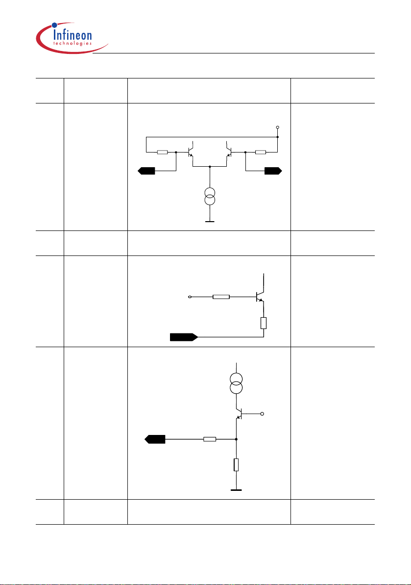
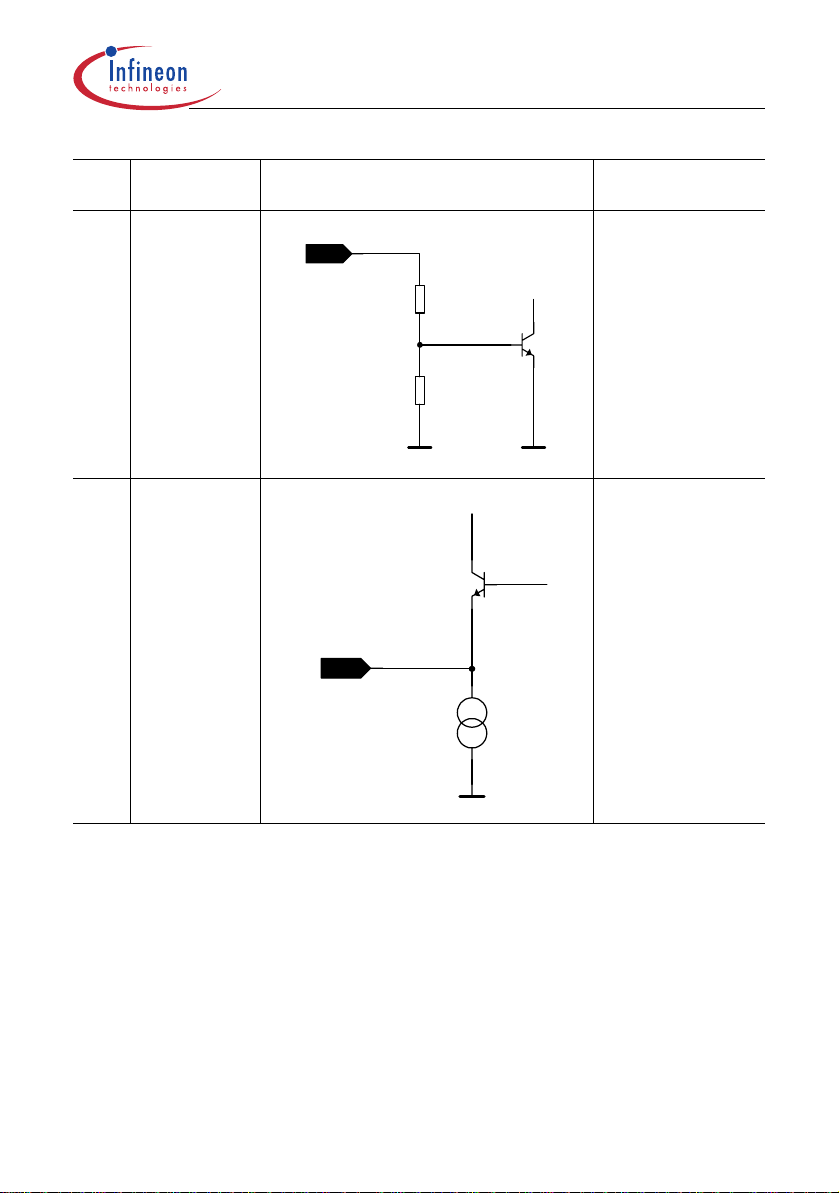
Pin
No.
1 CRST1 External Crystal
2 VCC 5V Supply
3 LNI LNA Input
Symbol Equivalent I/O Schematic Function
Connector 1
4.15V
1
50uA
57uA
3
500uA
4k
1k
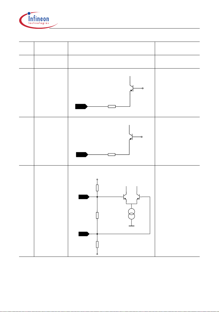
Preliminary Specification 8 V 1.1, 2004-10-20
TDA 5220
Pin
Symbol Equivalent I/O Schematic Function
Functional Description
No.
4 TAGC AGC Time Constant
4.3V
3uA
4
1k
1.4uA
1.7V
Control
5 AGND Analogue Ground
Return
6 LNO LNA Output
5V
1k
6
7 VCC 5V Supply
Preliminary Specification 9 V 1.1, 2004-10-20
TDA 5220
Pin
Symbol Equivalent I/O Schematic Function
Functional Description
No.
8
9
MI
MIX
2k 2k
8
400uA
Mixer Input
1.7V
Complementary
Mixer Input
9
10 AGND Analogue Ground
Return
11 FSEL 868/434 MHz
Operating
1.2V
11
750
Frequency Selector
2k
12 IFO 10.7 MHz IF Mixer
Output
300uA
2.2V
12
60
4.5k
13 DGND Digital Ground
Return
Preliminary Specification 10 V 1.1, 2004-10-20
TDA 5220
Pin
Symbol Equivalent I/O Schematic Function
Functional Description
No.
14 VDD 5V Supply (PLL
Counter Circuity)
15 MSEL ASK/FSK
Modulation Format
Sector
1.2V
15
40k
16 SSEL Data Slicer
Reference Level
Sector
1.2V
40k
Limiter Input
2.4V
17
16
LIM
18
LIMX
17
18
15k
330
15k
Complementary
Limiter Input
75uA
Preliminary Specification 11 V 1.1, 2004-10-20
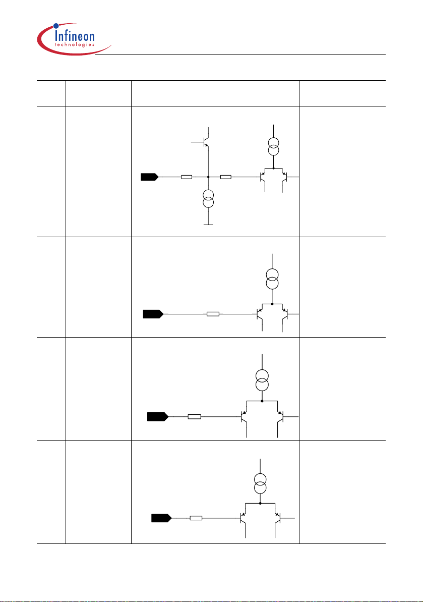
TDA 5220
Pin
Symbol Equivalent I/O Schematic Function
Functional Description
No.
19 SLP Data Slicer Positive
Input
15uA
19
100
3k
80µA
20 SLN Data Slicer
Negative Input
5uA
20
10k
21 OPP OpAmp
Noninverting Input
5uA
21
200
22 FFB Data Filter
Feedback Pin
5uA
22
Preliminary Specification 12 V 1.1, 2004-10-20
100k
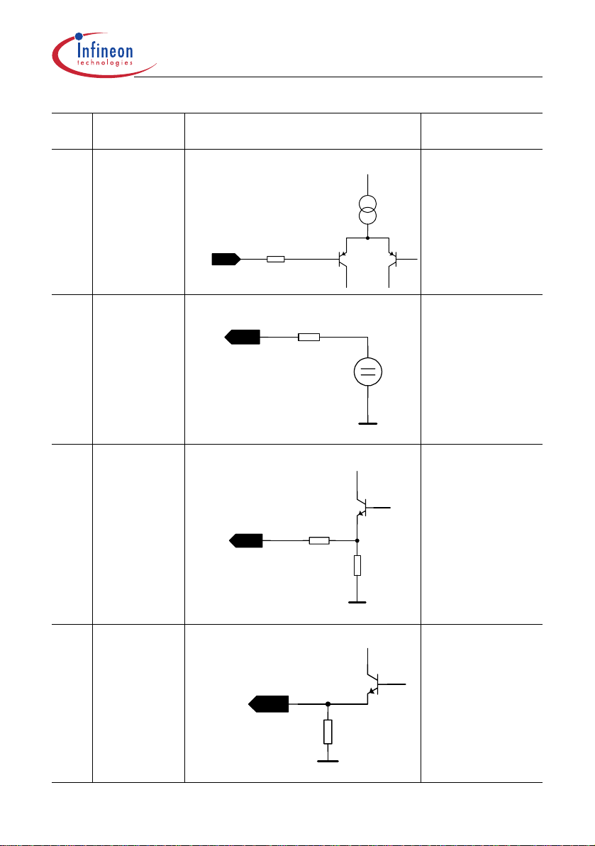
TDA 5220
Pin
Symbol Equivalent I/O Schematic Function
Functional Description
No.
23 THRES AGC Threshold
Input
5uA
23
10k
24 3VOUT 3V Reference
Output
24
20k
Ω
3.1V
25 DATA Data Output
25
500
40k
26 PDO Peak Detector
Output
26
446k
Preliminary Specification 13 V 1.1, 2004-10-20
TDA 5220
Pin
Symbol Equivalent I/O Schematic Function
Functional Description
No.
27 PDWN Power Down Input
27
220k
220k
28 CRST2 External Crystal
Connector 2
4.15V
28
50uA
Preliminary Specification 14 V 1.1, 2004-10-20
TDA 5220
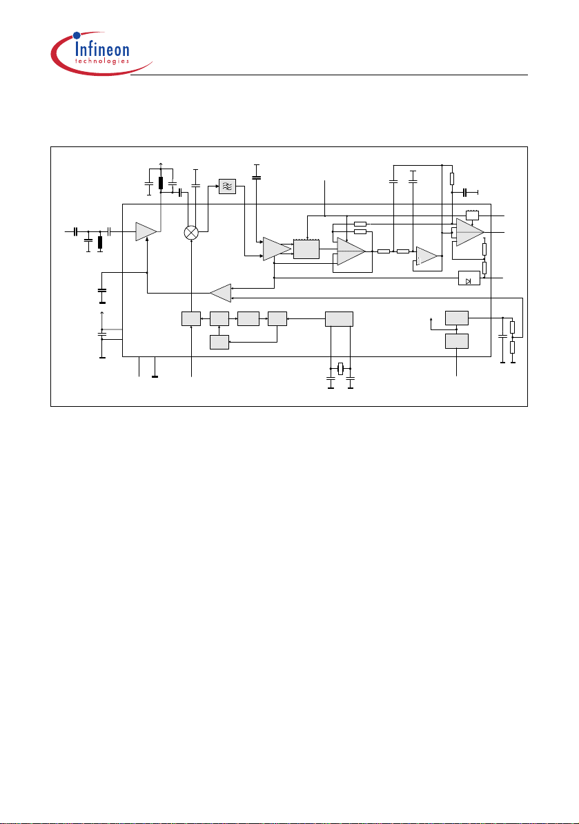
2.3 Functional Block Diagram
VCC
MI
68912 1718
LNI
3
TAGC
VCC
DGND
LNA
4
14
13
2,7 5,10
VCC AGND
RF
Figure 2 Block Diagram
IF
Filter
MIXLNO
IFO SLN
LIM LIMX
LIMITER
TDA 5220
OTA
: 1
VCO : 64
: 2
Loop
Filter
11
FSEL
Φ
DET
2.4 Functional Block Description
FSK
PLL Demod
MSEL
H=ASK
L=FSK
15
CRYSTAL
OSC
1
Crystal
-
+
-
ASK
+
FFB
FSK
28 27
Functional Description
OPP
SLP
22 21 19
20
16
SSEL
Logic
25
CM
DATA
+
CP
+
-
+
DATA-
SLICER
OP
-
PEAK
PDO
DETECTOR
26
THRES
23
U
REF
AGC
Reference
Bandgap
Reference
PDWN
3VOUT
24
2.4.1 Low Noise Amplifier (LNA)
The LNA is an on-chip cascode amplifier with a voltage gain of 15 to 20dB. The gain
figure is determined by the external matching networks situated ahead of LNA and
between the LNA output LNO (Pin 6) and the Mixer Inputs MI and MIX (Pins 8 and 9).
The noise figure of the LNA is approximately 3dB, the current consumption is 500µA.
The gain can be reduce d by approxi mately 18 dB. The swit ching poi nt of this AGC ac tion
can be determined externally b y applyi ng a thresh old volta ge at the THRES pin (Pin 23).
This voltage is compared internally with the received signal (RSSI) level generated by
the limiter circuitry. In case that the RSSI level is higher than the threshold voltage the
LNA gain is reduced and vice versa. The threshold voltage can be generated by
attaching a voltage divider between the 3VOUT pin (Pin 24) which provides a
temperature stable 3V output generated from the internal bandgap voltage and the
THRES pin as described in Section 3.1. The time constant of the AGC action can be
determined by connecting a capacitor to the TAGC pin (Pin 4) and should be chosen
along with the appropriate threshold voltage according to the intended operating case
and interference scena rio to be expe cted du ring ope ration. The optim um ch oice of AGC
time constant and the threshold voltage is described in Section 3.1.
Preliminary Specification 15 V 1.1, 2004-10-20
TDA 5220
Functional Description
2.4.2 Mixer
The Double Balanced Mixer down conve rts the i nput fre quenc y (RF) in th e range o f 40 0440MHz/810-870MHz to the interm ediate frequenc y (IF) at 10. 7MHz with a vo l-tage gain
of approximately 21 dB by utilising either high- or lo w-side injection of the lo ca l os cil la t or
signal. In case the mixer is interfaced only single-ended, the unused mixer input has to
be tied to ground vi a a c ap aci tor. The mixer is followed by a low pass fil ter w it h a c orn er
frequency of 20MHz in order to su ppress RF s ignals to appe ar at the IF output (IFO pin).
The IF output is internal ly c on si sti ng o f an em itte r fol lower that has a source i mped anc e
of approximately 330Ω to facilitate interfacing the pin directly to a standard 10.7MHz
ceramic filter without additional matching circuitry.
2.4.3 PLL Synthesizer
The Phase Locked Loo p syn thesi zer co nsist s of a VCO, an asy nchro nous d ivide r chain,
a phase detector with charge pump and a loop filter and is fully implemented on-chip.
The VCO is including sp iral ind uctors and vara ctor di odes. T he tu ning ran ge of the VCO
guarantee over production spread and the specified temperature range is 820 and
860MHz. The oscillator signal is fed both to the synthesiser divider chain and to the
downconverting mixer. In case of operation in the 400 to 440MHz range the signal is
divided by two before it is fed to the Mixer. Depending on whether high- or low-side
injection of the local oscillator is used, the receiving frequency ranges are 810 to
840MHz and 840 to 870MHz or 400 to 420MHz and 420 to 440MHz - see also Section
3.4. To be able to switch between two different frequency channels a divider ratio of
either 32 or 32.25 can be selected via the FSEL-Pin.
Table 2 FSEL-Pin Operating States
FSEL RF
Open 400-440MHz
GND 810-870MHz
2.4.4 Crystal Oscillator
The calculation of the value of the necessary crystal load capacitance is shown in
Section 3.3, the crystal frequency calculation is explained in Section 3.4.
2.4.5 Limiter
The Limiter is an AC coupled multistage amplifier with a cumulative gain of
approximately 80 dB that has a bandpass-characteristic centred around 10.7 MHz. It
has a typical input impedance of 330 Ω to allow for easy interfacing to a 10.7 MHz
ceramic IF filter. The limiter circuit also acts as a Receive Signal Strength Indicator
(RSSI) generator which produces a DC voltage that is directly proportional to the input
Preliminary Specification 16 V 1.1, 2004-10-20

TDA 5220
signal level as can be seen in Figure 4. This signal is used to demodulate ASKmodulated receive signals in the subsequent baseband circuitry. The RSSI output is
applied to the modulation format switch, to the Peak Detector input and to the AGC
circuitry.
In order to demodulate ASK signals the MSEL pin has to be in its ‘High‘-state as
described in the next chapter.
Functional Description
2.4.6 FSK Demodulator
To demodulate frequency shift keyed (FSK) signals a PLL circuit is used that is
contained fully on chip. The Limiter output differential signal is fed to the linear phase
detector as is the output of the 10.7 MHz center frequency VCO. The demodulator gain
is typically 200µV/kHz. The passive loop fil ter output that is com prised fully on chip is fed
to both the VCO and the modulation format switch described in more detail below. This
signal is representing the demodulated signal with low frequencies applied to the
demodulator demo dulated to l ogic zero an d high freque ncies demo dulated to lo gic ones.
However this is only valid in case the local os cillator is low- side injected to the mixer
which is applicable to receive frequencies above 840 or 420MHz. In case of receive
frequencies below 840 or 420MHz high frequencies are demodulated as logical zeroes
due to a sign inversion in the downconversion mixing process as the L0 is high-side
injected to the mixer. See also Section 3.4.
The modulation forma t switch i s actually a switchabl e amplifier wi th an AC gain o f 11 that
is controlled by the MSEL pin (Pin 15) as shown in the following table. This gain was
chosen to facilitate d etec tio n in the sub se que nt c irc uit s. Th e DC gai n is 1 i n ord er no t to
saturate the subsequent Data Filter wih the DC offset produced by the demodulator in
case of large frequency offsets of the IF signal. The resulting frequency characteristic
and details on the principle of operation of the switch are described in Section 3.6.
Table 3 MSEL Pin Operating States
MSEL Modulation Format
Open ASK
Shorted to ground FSK
The demodulator circuit is switched off in case of reception of ASK signals.
2.4.7 Data Filter
The data filter comprises an OP-Amp with a bandwidth of 100kHz used as a voltage
follower and two 100kΩ on-chip resistors . Along with two exte rnal capacitor s a 2nd order
Preliminary Specification 17 V 1.1, 2004-10-20

TDA 5220
Sallen-Key low pass filter is formed. The selection of the capacitor values is described
in Section 3.2.
Functional Description
2.4.8 Data Slicer
The data slicer is a fast comparator with a bandwidth of 100 kHz. This allows for a
maximum receive data r ate of up to 10 0kBaud . The maxim um achiev able da ta rate als o
depends on the IF F ilt er b andwidth and the lo cal oscillator tole ranc e values. Both inputs
are accessible. The output delivers a digital data signal (CMOS-like levels) for
subsequent circuits. A self-adjusting slicer-threshold on pin 20 its generated by a RCterm. In ASK-mode alte rnatively a sc aled value of t he voltage at th e PDO-output (approx .
87%) can be used as the s licer-th reshol d as sh own in Tab le 4. The data slicer threshol d
generation alternatives are described in more detail in Section 3.5.
Table 4 SSEL Pin Operating States
SSEL MSEL Selected Slicing Level (SL)
X Low external SL on Pin 20 (RC-term, e.g.)
High High external SL on Pin 20 (RC-term, e.g.)
Low High 87% of PDO-output (approx.)
2.4.9 Peak Detector
The peak detecto r gene rates a DC v oltage which is p roportio nal to the pe ak v alue o f the
receive data sign al. A capa citor is n ecessary . The inpu t is conn ected to th e out put of th e
RSSI-output of the Limiter, the output is connected to the PDO pin (Pin 26). This output
can be used as an indicator for the received signal strength to use in wake-up circuits
and as a reference for the data slicer in ASK mode. Note that the RSSI level is also
output in case of FSK mode.
2.4.10 Bandgap Reference Circuitry
A Bandgap Reference Circuit provides a temperature stable reference voltage for the
device. A power down mode is available to switch off all subcircuits which is controlled
by the PWDN pi n ( Pin 2 7) as sh own in the fo ll o win g t ab le. T h e s u pply current dra w n in
this case is typically 50nA.
Table 5 PDWN Pin Operating States
PDWN Operating State
Open or tied to ground Powerdown Mode
Tied to Vs Receiver On
Preliminary Specification 18 V 1.1, 2004-10-20

TDA 5220
3 Applications
3.1 Application Circuit
3VO UT
24 23
20kΩ
RSSI > U
RSSI < U
threshold
threshold
: I
load
: I
load
=4.2µA
= -1.5µA
TAGC
+ 3 .1 V
C5
R4
THRES
I
load
4
U
c
U
C
U
c
U
cma x
U
cmin
C18
R5
U
threshold
OTA
VCC
G ain control
voltage
:< 2.6V : G ain high
:> 2 .6V : G a in low
= VCC - 0.7 V
= 1.67V
Applications
R S S I (0.8 - 2 .8V )
LNA
Figure 3 LNA Automatic Gain Control Circuity
The LNA automatic gain control circuitry consists of an operational transimpedance
amplifier that is used to compare the received signal strength signal (RSSI) generated
by the Limiter with an externally provided threshold voltage U
. As shown in the
thres
following figure th e threshold volt age can have any value between approximately 0.8 and
2.8V to provide a switching point within the receive signal dynamic range.
This voltage U
is applied to the THRES pin (Pin 23 ) The thresh old voltage ca n be
thres
generated by attaching a voltage divider between the 3VOUT pin
(Pin 24) which provides a temperature stable 3V output generated from the internal
bandgap voltage and the THRES pin. If the RSSI level g enerated by the L imiter is h igher
than U
, the OTA generates a positi ve current I
thres
. This yields a voltage ris e on th e
load
TAGC pin (Pin 4). Otherwi se, the OTA generates a ne gat iv e cu rren t. These currents do
not have the same values in order to achiev e a fast-attack an d slow-release ac tion of the
Preliminary Specification 19 V 1.1, 2004-10-20

TDA 5220
Applications
AGC and are used to charge an extern al capac itor wh ich fin ally ge nerates the LNA gain
control voltage.
in high gain mode
3
2.5
2
1.5
Voltage Range
THRES
U
1
0.5
0
-120 -110 -100 -90 -80 -70 -60 -50 -40
RSSI Level
Input Level at LNA Input [dBm]
LNA always
RSSI Level Range
in low gain mode
LNA always
-30
Figure 4 RSSI Level and Permissive AGC Threshold Levels
The switching poi nt should be chosen accordin g to the in tended operating scenario . The
determination of the optimum point is described in the accompanying Application Note,
a threshold voltage level of 1.8V is apparently a via ble choice. It shoul d be noted that the
output of th e 3VOUT pin is capable of driving up to 50µA, but that the THRES pin input
current is only in the reg ion of 40nA. As the curren t drawn out of the 3VOUT pin is directly
related to the receiver power con sumptio n, the pow er divider resi stor s shoul d have hig h
impedance values. The sum of R1 and R2 has to be 600kΩ in order to yield 3V at the
3VOUT pin. R1 can thus be chosen as 240kΩ, R2 as 360kΩ to yield an overall 3VOUT
output current of 5µA
1)
and a threshold voltage of 1.8V
Note: If the LNA gain shall be kept in either high or low gain mode this has to be
accomplished by tying the THRES pin to a fixed voltage. In order to achieve high gain
mode operation, a voltage higher than 2.8V shall be applied to the THRES pin, such as
a short to the 3VOLT pin. In order to achieve low gain mode operati on THRES has t o be
connected to GND.
As stated above the capacitor connected to the TAGC pin is gen erat ing the gain contro l
voltage of the LNA due to the charging and discharging currents of the OTA and thus is
also responsible for the AGC time constant. As the charging and discharging currents
are not equal two differen t time constan ts will res ult. The time cons tant corr espondin g to
the charging process of the capacitor shall be chosen according to the data rate.
According to measuremen ts performed at Infine on the capacitor valu e should be greater
than 47nF.
1) note the 20kΩ resistor in series with the 3.1V internal voltage source
Preliminary Specification 20 V 1.1, 2004-10-20

TDA 5220
Applications
3.2 Data Filter Design
Utilising the on-board voltage follower and the two 100kΩ on-chip resistors a 2nd order
Sallen-Key low pass data filter can be constructed by adding 2 external capacitors
between pins 19 (SLP) and 22 (FFB) and to pin 21 (OPP) as depicted in the following
figure and described in the following formulas
C14 C12
22 21 19
R
F1 int
100k 100k
R
F2 int
Figure 5 Data Filter Design
with R
F1int=RF2int
=R
2
=
C
14
fR
2
π
3
1)
.
SLPOPPFFB
bQ
C
12
dB
b
=
fQR
4
π
dB
3
with
b
Q =
a
Q is the qualify factor of the poles where, in case of a Bessel filter a=1.3617, b=0.618
and thus Q=0.577
and in case of a Butter worth filter a=1.414, b=1
and thus Q=0.71
Example: Butter worth filter with f
=5kHz and R=100kΩ:
3dB
C14=450pF, C12=225pF
1) taken from Tietze/Schenk: Halbleiterschaltungstechnik, Springer Berlin, 1999
Preliminary Specification 21 V 1.1, 2004-10-20

TDA 5220
Applications
3.3 Crystal Load Capacitance Calculation
The value of the capacit or neces sary to ac hieve that the cry stal os cilla tor is opera ting at
the intended frequency is determined by the reactive part of the negative resistance of
the oscillator circu it as shown in Section 4.1.3 and by the c r ys tal spe cif ic ati ons giv en by
the crystal manufacturer.
C
S
CRST2
Xf
L
28
TDA521X
1
CRST1
can be
L
Crystal
Input
impedance
Z
1-28
Figure 6 Determination of Series Capacitance Vale for the Quartz Oscillator
The required series capacitor for a crystal with specified load capacitance C
calculated as
C
S
1
=
1
π
2
+
C
L
CL is the nominal load capacitance specified by the crystal manufacturer.
Example:
13.4 MHz: C
= 12 pF XL=1010 Ω CS = 5.9 pF
L
This value may be obtained by putting two capacitors in series to the crystal, such as
22pF and 8.2pF for 13.4MHz.
But please note that the calculated C
-value includes all parasitic.
S
3.4 Crystal Frequency Calculation
As described in Section 2.4.3 the operating range of the on-chi p VCO is wi de enoug h to
guarantee a receive frequency range between 810 and 870MHz or between 400 and
440MHz. The VCO sign al is divide d by 2 before applied to the mixer i n case of o peration
at 434MHz. This local oscillator signal can be used to downconvert the RF signals both
Preliminary Specification 22 V 1.1, 2004-10-20

TDA 5220
r
Applications
with high- or low-side injec tion at th e mixe r. Hig h-side inject ion of the local oscil lator ha s
to be used for receive frequencies between 810 and 840MHz or beteween 400 and
420MHz. In this case the local oscillator frequency is calculated by adding the IF
frequency (10.7 MHz) to the RF frequency. Thus the higher frequency of a FSKmodulated signal is demodulated as a logical zero (low).
Low-side injection has to be used for receive frequencies above 840 MHz or above
420 MHz. The local oscillator frequency is calculated by subtracting the IF frequency
(10.7 MHz) from the RF frequency then. In this case no sign-inversion occurs and the
higher frequency of a FSK-modu lated si gnal is demod ulated as a log ical one (hi gh). The
overall division ratios in the PLL are 3 2 or 64 d epend ing on wheth er the FSEL -pin is le ft
open or tied to ground.
Therefore the crystal frequency may be calculated by using the following formula:
with ƒ
f
QU
RF
=
receive frequency
RF
f
ƒLO local oscillator (PLL) frequency (ƒ
7.10±
± 10.7)
RF
ƒQU quartz crystal oscillator frequency
r ratio of local oscillator (PLL) frequency and crystal frequency as
shown in the subsequent table
Table 6 Dependence of PLL Overall Division Ratio on FSEL
FSEL Ratio r=(fLO/fQU)
open 32
GND 64
This yields the following exa mples :
FSEL is „Low“:
MHzMHz
7.104.868
f
=
QU
64
−
4015625.13
=
MHz
FSEL is „High“:
MHzMHz
7.102.434
f
=
QU
Preliminary Specification 23 V 1.1, 2004-10-20
32
−
=
MHz
234375.13

TDA 5220
Applications
3.5 Data Slicer Threshold Generation
The threshold of the data slicer can be generated using an external R-C integrator as
shown in Figure 7.
The time constant T
of this circuit including also the internal resistors R
A
F3int
and R
F4int
(see Figure 9) has to be significantly larger than the longest period of no signal change
within the data sequence.
T
L
In order to keep distortion low, the minimum value for R is 20kΩ.
has to be calculated as
T
A
=
+⋅
T
A
1
)(1
RRR
FF
int4int3
++
RRR
FF
int4int3
⋅+=⋅
FF
int4int3
...13)(113
ASKforCRRIIRC
and
T
A
R1, R
=
F3 int
RR
1
⋅
F
int4
1
, R
++
and C13 see also Figure 7 and .Figure 9
F4 int
C
RRR
FF
13
int4int3
=⋅
RRIIR
+
v
)(1
FF
int4int3
⋅
FSKforC
...13
2019
data
filter
U
threshold
data slicer
25
CM
Figure 7 Data Slicer Threshold Generation with External R-C Integrator
In case of ASK operation another possibility for threshold generation is to use the peak
detector in connection with an internal resistive divider and one capacitor as shown in
the following Figure 8. For selecting the peak detector as reference for the slicing level
a logic low as to be applied on the SSEL pin.
In case of MSEL is high (or open), which means that ASK-Mode is selected, a logic low
on the SSEL pin yields a logic high on the AND-output and thus the peak-detector is
selected (see Figure 9).
In case of FSK the MSEL-pin and furthermore the one input of the AND-gate is low, so
the peak detector can not be selected.
The capacitor value is depending on the coding scheme and the protocol used.
Preliminary Specification 24 V 1.1, 2004-10-20

TDA 5220
C
Pins:
peak detector
26
56k
U
390k
data slicer
threshold
25
CP
Applications
Figure 8 Data Slicer Threshold Generation Utilising the Peak Detector
3.6 ASK/FSK-Data Path Functional Description
The TDA5220 is containing an ASK/FSK switch which can be controlled via Pin 15
(MSEL). This switch is actually consisting of 2 operational amplifiers that are having a
gain of 1 in case of the ASK amplifier and a gain of 11 in case of the FSK amplifier in
order to achieve an appropriate demodulation gain characteristic. In order to
compensate for the DC-offse t generated es pecially in case of the FSK PLL demodu lator
there is a feedback connec tion between the thresho ld voltage of the bit slic er comparator
(Pin 20) to the negative input of the FSK switch amplifier.
In ASK-mode alternatively to the voltage at Pin 20 (SLN) a value of approx. 87% of the
peak-detector output-vo lta ge at Pin 26 (PDO) can be used as the s li cer -refe renc e le ve l.
The slicing reference level is generated by an internal voltage divider (R
T1int
, R
T2int
which is applied on the peak detector output.
The selection between these modes is controlled by Pin 16 (SSEL), as described in
Section 3.5.
This is shown in the following Figure 9.
Preliminary Specification 25 V 1.1, 2004-10-20
),

TDA 5220
F
R
T1 int
R
H=CP
L=CM
SSEL
56k
390k
T2
Applications
PDO
26
25
C15
100n
DATA Out
from RSSI Gen
(ASK signal)
FSK PLL Demodulator
0.18 mV/kHz
typ. 2 V
1.5 V ......2.5 V
MSEL
15
H=ASK
L=FSK
ASK/FSK Switch
Data F ilter
-
+
ASK
FSK
+
-
AC DC
R
300k
R
F4 int
30k
ASK mode: v=1
FSK mode: v=11
F3 int
R
F1 int
100k 100k
C12
R
F2 int
v = 1
192122 20
SLPOOPFFB SLN
C14
PEAK
DETECTOR
Comp
+
CP
CM
+
-
1
16
R1
C13
Figure 9 ASK/FSK mode datapath
3.7 FSK Mode
The FSK datapath has a bandpass characterisitc due to the feedback shown above
(highpass) and the data filter (lowpass). The lower cutoff frequency f2 is determined by
the external RC-combination. The upper cutoff frequency f3 is determined by the data
filter bandwidth.
The demodulation gain of the FSK PLL demodulator is 200µV/kHz. This gain is
increased by the g ai n v o f th e FSK switch, which is 11 . Th ere fore the resulting dyna mic
gain of this circ uit is 2 .2mV/kHz within the bandpas s. The g ain for th e DC conte nt of FSK
signal remains at 200µV/kHz. The cu t-off frequencies of the bandpas s have to be chosen
such that the spectrum of the data signal is influenced in an acceptable amount.
In case that the use r data is co ntaini ng long se quences of l ogica l zeroes th e effect of th e
drift-off of the bit slicer threshold voltage can be lowered if the offset voltage inherent at
the negative input of the slicer comparator (Pin20) is used. The comparator has no
hysteresis built in.
This offset voltage is generated by the bias current of the negative input of the
comparator (i.e. 20nA) running over the external resistor R. This voltage raises the
voltage appearing a t p in 20 (e.g . 1 mV with R = 100kΩ). In or der to obt ain b enefit of this
Preliminary Specification 26 V 1.1, 2004-10-20

TDA 5220
Applications
asymmetrical offset for the demodulation of long zeros the lower of the two FSK
frequencies should be chosen in the transmitter as the zero-symbol frequency.
In the following figure the shape of the above mentioned bandpass is shown.
gain (pin19)
v
v-3dB
20dB/dec -40dB/dec
3dB
0dB
DC
f1 f2 f3
0.18mV/kHz
2mV/kHz
f
Figure 10 Frequency characteristic in case of FSK mode
The cutoff frequencies are calculated with the following formulas:
f
=
1
2
π
is the 3dB cutoff frequency of the data filter - see Section 3.2.
f
3
1
3301
kR
Ω×
13
C
×
3301
kR
Ω+
11 ffvf ×=×=
112
ff33=
dB
Example:
R1 = 100kΩ, C13 = 47nF
This leads tof
Preliminary Specification 27 V 1.1, 2004-10-20
= 44Hz and f2 = 485Hz
1

TDA 5220
Applications
3.8 ASK Mode
In case the receiver is operated in ASK mode the datapath frequency charactersitic is
dominated by the data filter alone, thus it is lowpass shaped.The cutoff frequency is
determined by the external capacitors C
and C14 and the internal 100k resistors as
12
described in Section 3.2
0dB
-3dB
-40dB/dec
f3dB
f
Figure 11 Frequency characteristic in case of ASK mode
3.9 Principle of the Precharge Circuit
In case the data slicer threshold shall be generated with an external RC network as
described in Section 3.5 it is necessary to use large values for the capacitor C attached
to the SLN pin (pin 2 0) in orde r to achie ve long tim e constants . This re sults al so from th e
fact that the choice of the value for R1 connected between the SLP and SLN pins (pins
19 and 20) is lim ite d by the 330kΩ resist or app ea ring in p aral le l t o R 1 as c an b e s ee n i n
Figure 9. Apart from this a resis tor va lue of 10 0kΩ lead s to a vol tage o ffset of 1mv at th e
comparator input. The resulting startup time constant τ
()
τ
1
can be calculated with:
1
13330||1
CkR ×Ω=
In case R1 is chosen to be 100kΩ and C13 is chosen as 47nF this leads to
()
τ
1
msnFknFkk 6.3477747330||100
=×Ω=×ΩΩ=
When the device is turned on this time constant dominates the time necessary for the
device to be able to demodulate data properly. In the powerdown mode the capacitor is
only discharged by leakage currents.
Preliminary Specification 28 V 1.1, 2004-10-20

TDA 5220
Applications
In order to reduce the turn-on time in the presence of large values of C a precharge
circuit was included in the TDA5220 as shown in the following figure.
C18
20k
24
R4+R5=600k
R4
U2
+3.1V
U
23
Uc>Us
R5
threshold
OTA
-
Uc<Us
0 / 240uA
+
20
I
load
-
+
U2<2.4V : I=240uA
U2>2.4V : I=0
+2.4V
C13
R1
19
Uc
Data Filter
Us
ASK/FSK Switch
Figure 12 Principle of the precharge circuit
This circuit charg es the c apaci tor C13 w ith an inrus h curren t I
duration of T
until the vol tag e Uc appearing on the capacitor is equal to the voltage U
2
of typically 220µA for a
load
at the input of the data filter. This voltage is limited to 2.5V. As soon as these voltages
are equal or the duration T
is exceeded the precharge circuit is disabled.
2
τ2 is the time constant of the charging process of C18 which can be calculated as
s
τ
as the sum of R4 and R5 is sufficiently large and thus can be neglected. T
2202Ck ×Ω≈
can then be
2
calculated according to the following formula:
T
Preliminary Specification 29 V 1.1, 2004-10-20
ln
=
1
−
1
4.2
V
3
V
6.1
×≈
ττ
222

TDA 5220
The voltage transient during the charging of C2 is shown in the following figure:
Applications
U2
3V
2.4V
2
Figure 13 Voltage appearing on C18 during precharging process
The voltage appe aring on the c apacitor C13 co nnected to pin 20 is shown in the followin g
figure. It can be seen that due to the fact that it is charged by a constant current source
it exhibits is a lin ear inc rease in v olt age whi ch is lim ited to U
approximate operating point of the data filter input. The time constant appearing in this
case can be denoted as T3, which can be calculated with:
T2
= 2.5V which is also the
Smax
13
CU
×
max
S
T
=
3
220
A
Preliminary Specification 30 V 1.1, 2004-10-20
220
5.2
V
13
C
×=
A
µµ

TDA 5220
Uc
Us
T3
Figure 14 Voltage transient on capacitor C13 attached to pin 20
As an example the choice of C18 = 22nF and C13 = 47nF yields
= 0.44ms
τ
2
T2 = 0.71ms
T3 = 0.53ms
Applications
This means that in this case the inrush current could flow for a duration of 0.64ms but
stops already after 0.49m s when the U
chosen to be shorter than T
.
2
limit has been reac hed. T3 should always be
Smax
It has to be noted finally that during the turn-on duration T2 the overall device power
consumption is increased by the 220µA needed to charge C13.
The precharge circuit may be disabled if C18 is not equipped. This yields a T
zero. Note th at the sum of R
and R5 has to be 600kΩ in order to produce 3V at the
4
close to
2
THRES pin as this voltage is internally used also as the reference for the FSK
demodulator.
Preliminary Specification 31 V 1.1, 2004-10-20

TDA 5220
Reference
4 Reference
4.1 Electrical Data
4.1.1 Absolute Maximum Ratings
Attention: The maximum ratings may not be exceeded under any circumstances,
not even momentarily a nd in divi dual ly, a s p erma nent dam age to th e IC
may result. The AC/DC characteristic limits are not guaranteed.
Table 7 Absolute Maximum Ratings, T
#
Parameter Symbol Limit Values Unit Remarks
min. max.
1 Supply Voltage V
2 Junction Temperature T
3 Storage Temperature T
4 Thermal Resistance R
5 ESD integrity, all pins
excl. Pins 1,3, 6, 28
ESD integrity Pins
1,3,6,28
s
j
s
thJA
V
ESD
= -40 °C … +105 °C
amb
-0.3 5.5 V
-40 +125 °C
-40 +150 °C
114 K/W
+2
+1.5
kVkVHBM according to
MIL STD 883D,
method 3015.7
4.1.2 Operating Range
Within the operational range the IC operates as explained in the circuit description.
Currents flowing into the device are denoted as positive currents and vice versa. The
device parameters with ■ are not part of the product ion test, but ei ther verifie d by desig n
or measured in the Infineon Evalboard as described in Section 4.2.
Supply voltage: VCC = 4.5V .. 5.5V
Preliminary Specification 32 V 1.1, 2004-10-20

TDA 5220
Table 8 Operating Range,
#
Parameter Symbol Limit Values Unit Test Conditions/
1 Supply Current ISF868
2 Receiver Input Level
ASK
FSK, frequ. dev. ± 50kHz
3 LNI Input Frequency f
4 MI/X Input Frequency f
5 3dB IF Frequency Range
ASK
FSK
6 Powerdown Mode On PWDNON2VSV
7 Powerdown Mode Off PWDN
8 Gain Control Voltage,
LNA high gain state
9 Gain Control Voltage,
LNA low gain state
I
SF
I
SA
I
SA
RF
RF
MI
f
IF -3dB
V
THRES
V
THRES
434
868
434
in
T
= -40 °C … +105 °C
amb
min. max.
3.9
3.7
3.2
3.0
-106
-100
400/810 440/870 MHz
400/810 440/870 MHz
5
10.4
00.8V
OFF
2.8 V
00.7V
7.9
7.7
7.2
7.0
-13
-13
23
11
S
mA
mA
mA
mA
dBm
dBm
MHz
V
Notes
f
=868MHz, FSK Mode
RF
=434MHz, FSK Mode
f
RF
f
=868MHz, ASK Mode
RF
=434MHz, ASK Mode
f
RF
@source impedance
50Ω
BER 2E-3, average
power level, Manchester
encoded datarate 4kBit,
280KHz IF Bandwidth
Reference
L
■
■
■ Not part of the production test - either verified by design or measured in the Infineon
Evalboard as described in Section 4.2.
4.1.3 AC/DC Characteristics at T
AMB
= 25°C
AC/DC characteristics involve the spread of values guaranteed within the specified
voltage and ambient temperature range. Typical characteristics are the median of the
production. Currents flowing into the device are denoted as po-sitive currents and vice
versa. The device performan ce parameters marked with
■ are not part of the pro ductio n
test - either verified by design or measured in the Infineon Evalboard as described in
Section 4.2.
Preliminary Specification 33 V 1.1, 2004-10-20

TDA 5220
Table 9 AC/DC Characteristics with TA 25°C, V
#
Parameter Symbol Limit Values Unit Test Conditions/
min. typ. max.
=4.5 ... 5.5 V
VCC
Notes
SUPPLY
Supply Current
1 Supply current,
standby mode
2 Supply current, device
operating in 868 MHz
range, FSK mode
3 Supply current, device
operating in 434 MHz
range, FSK mode
4 Supply current, device
operating in 868 MHz
range, ASK mode
5 Supply current, device
operating in 434 MHz
range, ASK mode
I
S PDWN
I
SF 868
I
SA 434
I
SA 868
I
SA 434
50 100 nA Pin 27 (PDWN)
open or tied to 0 V
5.1 5.9 6.7 mA Pin 11 (FSEL) tied to
GND, Pin 15 (MSEL)
tied to GND
4.9 5.7 6.5 mA Pin 11 (FSEL) open,
Pin 15 (MSEL) tied
to GND
4.4 5.2 6 mA Pin 11 (FSEL) tied to
GND, Pin 15
(MSEL) open
4.2 5. 5.8 mA Pin 11 (FSEL) open,
Pin 15 (MSEL) open
Reference
L
LNA
Signal Input LNI (PIN 3), V
1 Average Power Level
at BER = 2E-3
(Sensitivity)
2 Average Power Level
at BER = 2E-3
(Sensitivity) FSK
3 Input impedance,
= 434 MHz
f
RF
4 Input impedance,
f
= 869 MHz
RF
5 Input level @ 1dB
compression
Preliminary Specification 34 V 1.1, 2004-10-20
>2.8V, high ga i n mode
THRES
RF
in
RF
in
S
11 LNA
S
11 LNA
P1dB
0.873 / -34.7 deg ■
0.738 / -73.5 deg ■
LNA
-110 dBm Manchester
encoded datarate
4kBit, 280kHz IF
Bandwidth
-103 dBm Manchester enc.
datarate 4kBit,
280kHz IF Bandw., ±
50kHz pk. dev.
-15 dBm ■
■
■

TDA 5220
#
Parameter Symbol Limit Values Unit Test Conditions/
Notes
6 Input 3rd order intercept
point f
7 Input 3
point f
= 434 MHz
RF
rd
order intercept
= 869 MHz
RF
8 LO signal feedthrough
at antenna port
Signal Output LNO (PIN 6), V
1 Gain f
2 Gain f
= 434 MHz S
RF
= 869 MHz S
RF
3 Output impedance,
= 434 MHz
f
RF
4 Output impedance,
= 869 MHz
f
RF
5 Voltage Gain Antenna
to MI f
= 434 MHz
RF
6 Voltage Gain Antenna
to MI f
Signal Input LNI, V
= 869 MHz
RF
=GND, lwo gain mode
THRES
1 Input impedance,
= 434 MHz
f
RF
2 Input impedance,
= 869 MHz
f
RF
3 Input level @ 1dB C. P.
= 434 MHz
f
RF
4 Input level @ 1dB C. P.
f
= 869 MHz
RF
rd
point f
point f
order intercept
= 434 MHz
RF
rd
order intercept
= 869 MHz
RF
= 434 MHz S
RF
= 869 MHz S
RF
=GND, lwo gain mode
THRES
5 Input 3
6 Input 3
Signal Output LNO, V
1 Gain f
2 Gain f
3 Output impedance,
= 434 MHz
f
RF
min. typ. max.
IIP3
LNA
IIP3
LNA
LO
LNI
>2.8V, high gain mode
THRES
21 LNA
21 LNA
S
22 LNA
S
22 LNA
G
AntMI
G
AntMI
S
11 LNA
S
11 LNA
P1dB
P1dB
IIP3
IIP3
21 LNA
21 LNA
S
22 LNA
LNA
LNA
LNA
LNA
1.509/ 138.2 deg ■
1.419/ 101.7 deg ■
0.886 / -12.9 deg ■
0.866 / -24.2 deg ■
0.873 / -34.7 deg ■
0.738 / -73.5 deg ■
0.183 / 140.6 deg ■
0.179 / 109.1 deg ■
0.897 / -13.6 deg ■
-10 dBm mat ched input ■
-14 dBm mat ched input ■
-73 dBm ■
42 dB
40 dB
-18 dBm mat ched input ■
-6 dBm matched input ■
-10 dBm mat ched input ■
-5 dBm matched input ■
Reference
L
Preliminary Specification 35 V 1.1, 2004-10-20

TDA 5220
#
Parameter Symbol Limit Values Unit Test Conditions/
Notes
4 Output impedance,
= 869 MHz
f
RF
5 Voltage Gain Antenna
to MI f
= 434 MHz
RF
6 Voltage Gain Antenna
to MI f
= 869 MHz
RF
Signal 3VOUT (PIN 24)
1 Output voltage V
2 Current out I
Signal THRES (PIN 23)
1 Input Voltage range V
2 LNA low gain mode V
3 LNA high gain mode V
4 Current in I
Signal TAGC (PIN 4)
1 Current out,
LNA low gain state
2 Current in,
LNA high gain state
S
22 LNA
G
AntMI
G
AntMI
3VOUT
3VOUT
THRES
THRES
THRES
THRES_in
I
TAGC_out
I
TAGC_in
min. typ. max.
0.868 / -26.3 deg ■
22 dB
19 dB
2.9 3.1 3.3 V 3VOUT Pin open
-3 -5 -10 µA see Section 4.1
0V
3V
5nA ■
-3.6 -4.2 -5.5 µA RSSI > V
11.62.2µARSSI < V
-1 V see Section 4.1
S
0V
-1 V or shorted to Pin 24
S
Reference
L
THRES
THRES
MIXER
Signal Input MI/MIX (PINS 8/9)
1 Input impedance,
= 434 MHz
f
RF
2 Input impedance,
f
= 869 MHz
RF
rd
point f
point f
order intercept
= 434 MHz
RF
rd
order intercept
= 869 MHz
RF
3 Input 3
4 Input 3
S
11 MIX
S
11 MIX
IIP3
IIP3
Signal Output IFO (PIN 12)
1 Output impedance Z
2 Conversion Voltage
Gain f
= 434 MHz
RF
IFO
G
MIX
Preliminary Specification 36 V 1.1, 2004-10-20
0.942 / -14.4 deg ■
0.918 / -28.1 deg ■
MIX
MIX
-28 dBm ■
-26 dBm ■
330 Ω ■
19 dB

TDA 5220
#
Parameter Symbol Limit Values Unit Test Conditions/
Notes
3 Conversion Voltage
Gain f
= 869 MHz
RF
min. typ. max.
G
MIX
18 dB
LIMITER
Signal Input LIM/X (PINS 17/18)
1 Input Impedance Z
2 RSSI dynamic range DR
3 RSSI linearity LIN
4 Operating frequency
(3dB points)
f
LIM
LIM
264 330 396 Ω ■
RSSI
RSSI
70 dB
±1dB ■
5 10.7 23 MHz ■
DATA FILTER
1 Useable bandwidth BW
FILT
2 RSSI Level at Data
RSSI
Filter Output SLP,
RFIN=-103dBm
3 RSSI Level at Data
RSSI
Filter Output SLP,
=-30dBm
RF
IN
BB
low
high
100 kHz ■
1.1 V LNA in high gain
mode at 868 MHz
2.65 V LNA in high gain
mode at 868 MHz
Reference
L
SLICER
Signal Output DATA (PIN 25)
1 Maximum Datarate DR
2 LOW output voltage V
3 HIGH output voltage V
max
SLIC_L
SLIC_HVS
00.1V
1.3
-
Slicer, Negative Input (PIN 20)
1 Precharge Current Out I
PCH_SLN
-100 -220 -300 µA see Section 4.2.
Preliminary Specification 37 V 1.1, 2004-10-20
100 kBps NRZ, 20pF
VS-1 VS-
V output
0.7
capacitive loading
current=200µA
■

TDA 5220
#
Parameter Symbol Limit Values Unit Test Conditions/
min. typ. max.
Notes
PEAK DETECTOR
Signal Output PDO (PIN 26)
1 Load current I
2 Internal resistive load R 357 446 535 kΩ
load
-500 µA static load current
must not exceed
-500µA
CRYSTAL OSCILLATOR
Signals CRSTL 1, CRSTL 2 (PINS 1/28)
1 Operating frequency f
2 Input Impedance
~13MHz
@
3 Serial Capacity
~13MHz
@
CRSTL
Z
1-28
C
S10
6 14 MHz fundamental mode,
-600 +
j 1010
=C1 5.9 pF ■
series resonance
Ω ■
ASK/FSK Signal Switch
Signal MSEL (PIN 15)
1 ASK Mode V
2 FSK Mode V
3 Input Bias Current
MSEL
MSEL
MSEL
I
MSEL
1.4 4 V or open
00.2V
-11 19 µA MSEL tied to GND
Reference
L
FSK DEMODULATOR
1 Demodulation Gain G
2 Useable IF Bandwidth BW
FMDEM
IFPLL
200 µV/
kHz
10.2 10.7 11.2 MHz
POWER DOWN MODE
Signal PDWN (PIN 27)
1 Powerdown Mode On PWDN
2 Powerdown Mode Off PWDN
Preliminary Specification 38 V 1.1, 2004-10-20
2.8 V
ON
00.8V
Off
V
S

TDA 5220
#
Parameter Symbol Limit Values Unit Test Conditions/
Notes
used crystal
3 Input bias current
PDWN
4 Start-up Time until
valid IF signal is
I
PDWN
T
SU
min. typ. max.
19 µA Power On Mode
<1 ms depends on the
detected
VCO MULTIPLEXER
Signal FSEL (PIN 11)
1f
range 434 MHz V
RF
range 869 MHz V
2f
RF
3 Input bias current
FSEL
FSEL
FSEL
I
FSEL
1.4 4 V or open
00.2V
-160 -200 -240 µA FSEL tied to GND
DATA-SLICER REFERENCE-LEVEL
Signal SSEL (PIN 16), ASK-Mode
1 Slicer-Reference is
voltage at Pin 20 (SLN)
2 Slicer-Reference is
approx. 87% of the
voltage at Pin 26
(PDO)
3 Input bias current
SSEL
V
SSEL
V
SSEL
I
SSEL
1.4 4 V or open
00.2V
-10 -19 µA SS EL tied to GND
Reference
L
■ Not part of the production test - either verified by design or measured in the Infineon
Evalboard as described in Section 4.2.
Preliminary Specification 39 V 1.1, 2004-10-20

TDA 5220
4.1.4 AC/DC Characteristics at T
= -40 to 105°C
AMB
Reference
Currents flowing into the device are denoted as positive currents and vice versa.
Table 10 AC/DC Characteristics with T
#
Parameter Symbol Limit Values Unit Test Conditions/
min. typ. max.
= -40°C ...+105°C, V
AMB
Notes
=4.5 ... 5.5 V
VCC
SUPPLY
Supply Current
1 Supply current,
standby mode
2 Supply current,
device operating in
868 MHz range, FSK
mode
3 Supply current,
device operating in
434 MHz range, FSK
mode
4 Supply current,
device operating in
868 MHz range, ASK
mode
5 Supply current,
device operating in
434 MHz range, ASK
mode
Signal Input 3VOUT (PIN 24)
1 Output voltage V
2 Current out I
Signal THRES (PIN 23)
1 Input Voltage range V
2 LNA low gain mode V
3 LNA high gain mode V
4 Current in I
Signal TAGC (PIN 4)
1 Current out,
LNA low gain state
I
S PDWN
I
SF 868
I
SA 434
I
SA 868
I
SA 434
3VOUT
3VOUT
THRES
THRES
THRES
THRES_in
I
TAGC_out
50 400 nA Pin 27 (PDWN) open
or tied to 0 V
3.9 5.9 7.9 mA Pin 11 (FSEL) tied to
GND, Pin 15 (MSEL)
tied to GND
3.7 5.7 7.7 mA Pin 11 (FSEL) open,
Pin 15 (MSEL) tied
to GND
3.2 5.2 7.2 mA Pin 11 (FSEL) tied to
GND, Pin 15
(MSEL) open
3 5. 7 mA Pin 11 (FSEL) open,
Pin 15 (MSEL) open
2.9 3.1 3.3 V 3VOUT Pin open
-3 -5 -10 µA see Section 4.1
0V
-1 V see Section 4.1
S
0V
3V
-1 V or shorted to Pin 24
S
5nA
-1 -4.2 -8 µA RSSI > V
THRES
■
■
Preliminary Specification 40 V 1.1, 2004-10-20

TDA 5220
#
Parameter Symbol Limit Values Unit Test Conditions/
Notes
2 Current in, LNA high
gain state
V
TAGC_in
min. typ. max.
0.5 1.5 5 µ A RSSI < V
MIXER
1 Conversion Voltage
Gain f
= 434 MHz
RF
2 Conversion Voltage
Gain f
= 868 MHz
RF
G
MIX
G
MIX
+19 dB
+18 dB
LIMITER
Signal Input LIM/X (PINS 17/18)
1 RSSI dynamic range DR
2 RSSI Level at Data
RSSI
Filter Output SLP,
RF
= -103dBm
IN
3 RSSI Level at Data
RSSI
Filter Output SLP,
= -30dBm
RF
IN
RSSI
low
high
70 dB
1.1 V LNA in high gain
mode at 868 MHz
2.65 V LNA in high gain
mode at 868 MHz
Reference
■
THRES
DATA FILTER
Slicer, Signal Output DATA (PIN 25)
1 Maximum Datarate DR
2 LOW output voltage V
3 HIGH output voltage V
max
SLIC_L
SLIC_HVS
00.1V
1.5
-
Slicer, Negative Input (PIN 20)
1 Precharge Current
Out
I
PCH_SLN
-100 -220 -300 µA see Section 4.2
Preliminary Specification 41 V 1.1, 2004-10-20
100 kBps NRZ, 20pF
VS-1 VS-
V output
0.5
capacitive loading
■
current=200µA

TDA 5220
#
Parameter Symbol Limit Values Unit Test Conditions/
min. typ. max.
Notes
PEAK DETECTOR
Signal Output PDO (PIN 26)
1 Load current I
2 Internal resistive load R 356 446 575 kΩ
load
-400 µA static load current
must not exceed
-500µA
CRYSTAL OSCILLATOR
Signals CRSTL 1, CRSTL 2 (PINS 1/28)
1 Operating frequency f
CRSTL
6 14 MHz fundamental mode,
series resonance
ASK/FSK Signal Switch
Signal MSEL (PIN 15)
1 ASK Mode V
2 FSK Mode V
3 Input bias current
MSEL
MSEL
MSEL
I
MSEL
1.4 4 V or open
00.2V
-11 -20 µA MSEL tied to GND
Reference
■
FSK DEMODULATOR
1 Demodulation Gain G
2 Useable IF
Bandwidth
FMDEM
BW
IFPLL
200 µV/
kHz
10.2 10.7 11.2 MHz
POWER DOWN MODE
Signal PDWN (PIN 27)
1 Powerdown Mode On PWDN
2 Powerdown Mode Off PWDN
Preliminary Specification 42 V 1.1, 2004-10-20
2.8 V
ON
00.8V
Off
V
S

TDA 5220
#
Parameter Symbol Limit Values Unit Test Conditions/
Notes
crystal
3 Start-up Time until
valid signal is
detected at IF
min. typ. max.
T
SU
<1 ms depends on the used
VCO MULTIPLEXER
Signal FSEL (PIN 11)
1f
range 434 MHz V
RF
range 869 MHz V
2f
RF
3 Input bias current
FSEL
FSEL
FSEL
I
FSEL
1.4 4 V or open
00.2V
-110 -200 -340 µA FSEL tied to GND
DATA-SLICER REFERENCE-LEVEL
Signal SSEL (PIN 16), ASK-Mode
1 Slicer-Reference is
voltage at Pin 20
(SLN)
2 Slicer-Reference is
approx. 87% of the
voltage at Pin 26
(PDO)
3 Input bias current
SSEL
V
SSEL
V
SSEL
I
SSEL
1.4 4 V or open
00.2V
-11 -20 µA SSEL tied to GND
Reference
■
■ Not part of the production test - either verified by design or measured in the Infineon
Evalboard as described in Section 4.2.
4.2 Test Circuit
The device performance parameters marked with ■ in Section 4.1 wer e ei th er ve rif ied
by design or measured on an Infineon evaluation board. This evaluation board can be
obtained together with evaluation boards of the accompanying transmitter device
TDK5110 in an evaluation kit that may be ordered on the INFINEON Webpage
www.infineon.com/Products. More information on the kit is available on request.
Preliminary Specification 43 V 1.1, 2004-10-20

TDA 5220
Figure 15 Schematic of the Evaluation Board
4.3 Test Board Layouts
Reference
Figure 16 Top Side of the Evaluation Board
Preliminary Specification 44 V 1.1, 2004-10-20

TDA 5220
Figure 17 Bottom Side of the Evaluation Board
Reference
Figure 18 Component Placement on the Evaluation Board
Preliminary Specification 45 V 1.1, 2004-10-20

TDA 5220
Reference
4.4 Bill of Materials
The following components are necessary for evaluation of the TDA5220.
Table 11 Bill of Materials (cont’d)
Ref. Value 434MHz Value 868MHz Specification
C1 1pF 1pF 0805, COG, +/-0.1pF
C2 4.7pF 3.9pF 0805, COG, +/-0.1pF
C3 6.8pF 5.6pF 0805, COG, +/-0.1pF
C4 100pF 100pF 0805, COG, +/-5%
C5 47nF 47nF 1206, X7R, +/-10%
C6 10nH 3.9pF Toko, PTL2012-F10N0G
C7 100pF 100pF 0805, COG, +/-5%
C8 33pF 22pF 0805, COG, +/-5%
C9 100pF 100pF 0805, COG, +/-5%
C10 10nF 10nF 0805, X7R, +/-10%
C11 10nF 10nF 0805, X7R, +/-10%
C12 220pF 220pF 0805, COG, +/-5%
C13 47nF 47nF 0805, X7R, +/-10%
C14 470pF 470pF 0805, COG, +/-5%
C15 47nF 47nF 0805, COG, +/-5%
C16 8.2pF 8.2 pF 0805, COG, +/-0.1pF
C17 18pF 18pF 0805, COG, +/-1%
C18 22nF 22nF 0805, X7R, +/-5%
C21 100nF 100nF 1206, X7R, +/-10%
IC1 TDA5220 TDA5220 Infineon
L1 15nH 3.3nH Toko, PTL2012-F15N0G
L2 8.2pF 3.9 pF 0805, COG, +/-0.1pF
Q1 13.234375 MHz 13.4015625 MHz 1053-922
Q2 SFE_10.7MA5-A SFE_10.7MA5-A Murata
R1 100kΩ 100kΩ 0805, +/-5%
R4 240kΩ 240kΩ 0805, +/-5%
R5 360kΩ 360kΩ 0805, +/-5%
Preliminary Specification 46 V 1.1, 2004-10-20

TDA 5220
Reference
Ref. Value 434MHz Value 868MHz Specification
R6 10kΩ 10kΩ 0805, +/-5%
S1 STL_2POL STL_2POL 2-pole pin connector
S2 SOL_JUMP SOL_JUMP SOL_JUMP
S3 SOL_JUMP SOL_JUMP SOL_JUMP
S6 SOL_JUMP SOL_JUMP SOL_JUMP
X1 STL_2POL STL_2POL 2-pole pin connector
X2 A107-900A (1.6mm
gold plated)
X3 A107-900A (1.6mm
gold plated)
A107-900A (1.6mm
gold plated)
A107-900A (1.6mm
gold plated)
INPUT OUTPUT
ENTERPRISE CORP
INPUT OUTPUT
ENTERPRISE CORP
Please note that in case of opera tion at 434M Hz a capac itor has to be so lder ed in place
L2 and an inductor in place C6.
Preliminary Specification 47 V 1.1, 2004-10-20

TDA 5220
5 Package Outlines
Package Outlines
P_TSSOP_28.eps
Figure 19 <Dev_Package1>
Table 12 Order Information
Type Ordering Code Package
TDA 5220 Q67100-H2049 <Dev_Package1>
You can find all of our packages, sorts of packing and others in our
Infineon Internet Page “Products”: http://www.infineon.com/products.
SMD = Surface Mounted Device
Preliminary Specification 48 V 1.1, 2004-10-20
Dimensions in mm

TDA 5220
List of Tables Page
Table 1 Pin Defintion and Function. . . . . . . . . . . . . . . . . . . . . . . . . . . . . . . . . . . 8
Table 2 FSEL-Pin Operating States . . . . . . . . . . . . . . . . . . . . . . . . . . . . . . . . . 16
Table 3 MSEL Pin Operating States. . . . . . . . . . . . . . . . . . . . . . . . . . . . . . . . . 17
Table 4 SSEL Pin Operating States . . . . . . . . . . . . . . . . . . . . . . . . . . . . . . . . . 18
Table 5 PDWN Pin Operating States . . . . . . . . . . . . . . . . . . . . . . . . . . . . . . . . 18
Table 6 Dependence of PLL Overall Division Ratio on FSEL. . . . . . . . . . . . . . 23
T
Table 7 Absolute Maximum Ratings,
Table 8 Operating Range,
T
= -40 °C … +105 °C . . . . . . . . . . . . . . . . . . . . 33
amb
Table 9 AC/DC Characteristics with T
Table 10 AC/DC Characteristics with T
Table 11 Bill of Materials. . . . . . . . . . . . . . . . . . . . . . . . . . . . . . . . . . . . . . . . . . . 46
Table 12 Order Information. . . . . . . . . . . . . . . . . . . . . . . . . . . . . . . . . . . . . . . . . 48
= -40 °C … +105 °C. . . . . . . . . . . . 32
amb
25°C, V
A
= -40°C ...+105°C, V
AMB
=8.5V /. . . . . . . . . . . . . . . . 34
VCC
=5.5V . . . . 40
VCC
Preliminary Specification 49 V 1.1, 2004-10-20

TDA 5220
List of Figures Page
Figure 1 Pin Configuration . . . . . . . . . . . . . . . . . . . . . . . . . . . . . . . . . . . . . . . . . . 7
Figure 2 Block Diagram . . . . . . . . . . . . . . . . . . . . . . . . . . . . . . . . . . . . . . . . . . . 15
Figure 3 LNA Automatic Gain Control Circuity. . . . . . . . . . . . . . . . . . . . . . . . . . 19
Figure 4 RSSI Level and Permissive AGC Threshold Levels . . . . . . . . . . . . . . 20
Figure 5 Data Filter Design . . . . . . . . . . . . . . . . . . . . . . . . . . . . . . . . . . . . . . . . 21
Figure 6 Determination of Series Capacitance Vale for the Quartz Oscillator. . 22
Figure 7 Data Slicer Threshold Generation with External R-C Integrator . . . . . 24
Figure 8 Data Slicer Threshold Generation Utilising the Peak Detector . . . . . . 25
Figure 9 ASK/FSK mode datapath. . . . . . . . . . . . . . . . . . . . . . . . . . . . . . . . . . . 26
Figure 10 Frequency characteristic in case of FSK mode . . . . . . . . . . . . . . . . . . 27
Figure 11 Frequency characteristic in case of ASK mode. . . . . . . . . . . . . . . . . . 28
Figure 12 Principle of the precharge circuit . . . . . . . . . . . . . . . . . . . . . . . . . . . . . 29
Figure 13 Voltage appearing on C18 during precharging process. . . . . . . . . . . . 30
Figure 14 Voltage transient on capacitor C13 attached to pin 20 . . . . . . . . . . . . 31
Figure 15 Schematic of the Evaluation Board . . . . . . . . . . . . . . . . . . . . . . . . . . . 44
Figure 16 Top Side of the Evaluation Board . . . . . . . . . . . . . . . . . . . . . . . . . . . . 44
Figure 17 Bottom Side of the Evaluation Board. . . . . . . . . . . . . . . . . . . . . . . . . . 45
Figure 18 Component Placement on the Evaluation Board. . . . . . . . . . . . . . . . . 45
Figure 19 P-TSSOP-28-1. . . . . . . . . . . . . . . . . . . . . . . . . . . . . . . . . . . . . . . . . . . 48
Preliminary Specification 50 V 1.1, 2004-10-20

www.infineon.com
Published by Infineon Technologies AG
 Loading...