


现货库存、技术资料、百科信息、热点资讯,精彩尽在鼎好!
Jens Eju
ry July 13, 2006 San Jose, CA
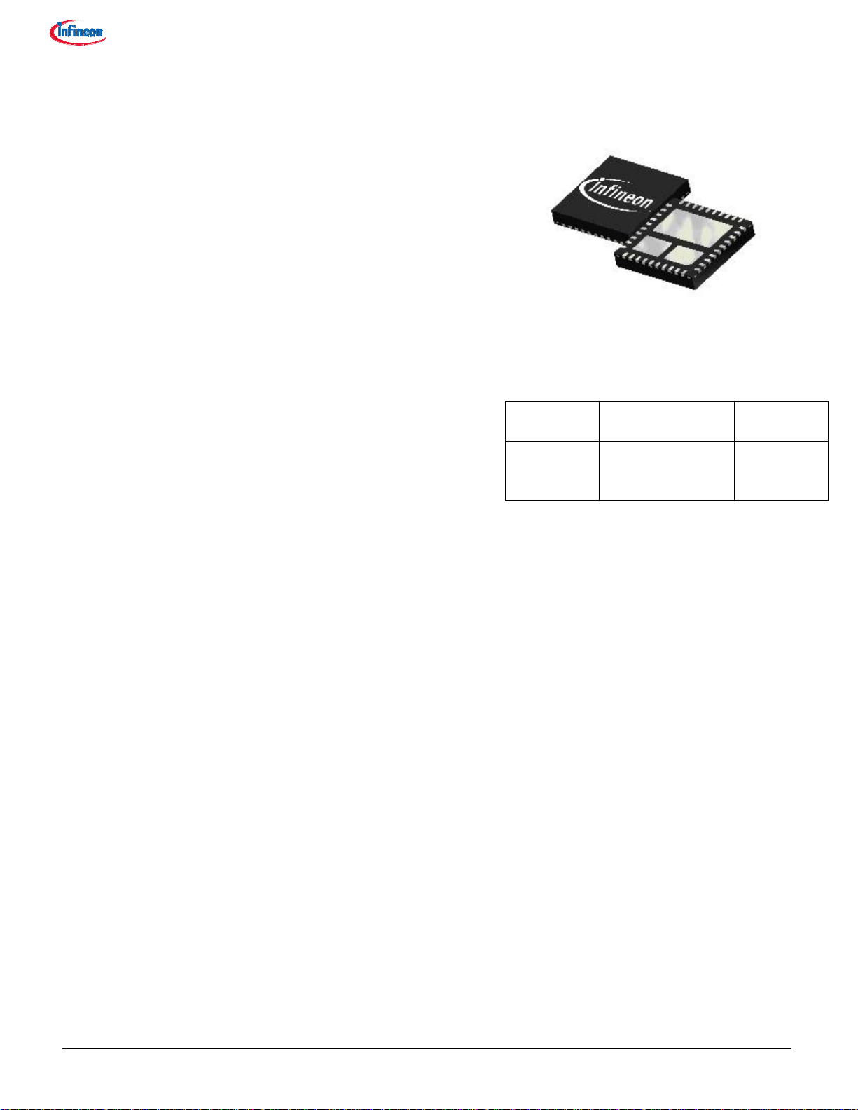
Data Sheet
High-Performance DrMOS
6mm x 6mm x 0.8mm IQFN
TDA21211- Data Sheet
August - 2009
Published by Infineon Technologies AG
http://www.infineon.com/DCDC
Power Management & Drive
Data Sheet
Never stop thinking
.
Page 1 of 20
TDA21211
6x6 QFN High-Performance DrMOS
Features:
• Intel compliant DrMOS, Power MOSFET and
Driver in one package
• For Synchronous Buck - step down voltage
applications
• Maximum Average Current of 35A
• Wide input voltage range +5V to +30V
• Low power dissipation
• Extremely fast switching technology for
improved performance at high switching
frequencies (>1MHz)
• Remote Driver Disable function
Type Package Marking
6x6x0.8mm3
TDA21211
PG-IQFN-40-1
TDA21211
• Switching Modulation (SMOD#) of low side
MOS
• Includes active PMOS structure as integrated
bootstrap circuit for reduced part count
• Shoot through protection
• +5V High and Low Side Driving voltage
• Compatible to standard PWM controller ICs with
+3.3 and 5V logic
• Three-State PWM input functionality
• Small Package: IQFN40 (6 x 6 x 0.8 mm3)
• RoHS Compliant
Applications:
• Desktop and Server
VR11.X and VR12 Vcore
and non-Vcore buckconverters
• Network and Telecom
processor VR
• Single Phase and MultiPhase POL
• CPU/GPU Regulation in
Notebook, Graphics Cards,
and Gaming
• Voltage Modules requiring
high power density
• Memory (DDR2/3)
Data Sheet
Page 2 of 20
TDA21211
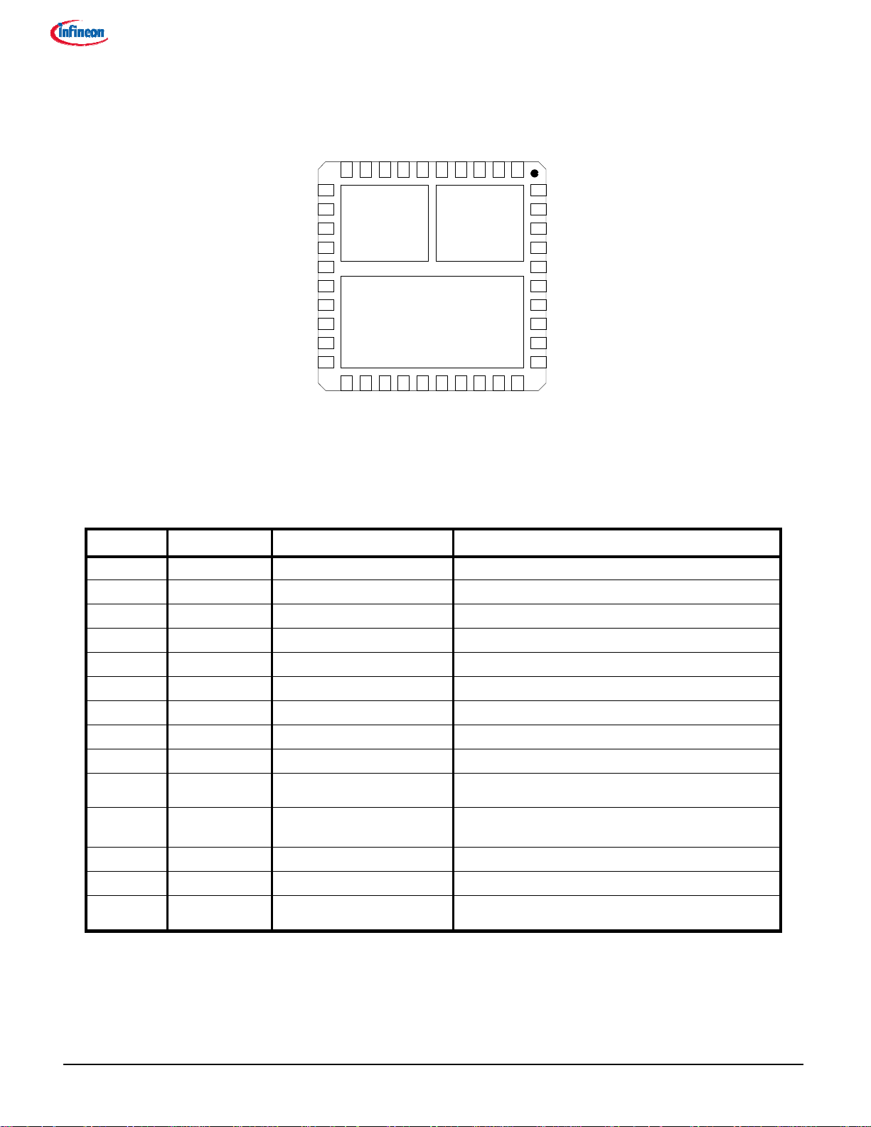
Pinout
VIN
VIN
VIN
VIN
VIN
VIN
VIN
VIN
VSWH
VSWH
PGND
PGND
PGND
PGND
PGND
PGND
PGND
PGND
PGND
PGND
VIN
VIN
VIN
VIN
11
12
13
14
15
16
17
18
19
20
22 23 24 25 26 27
21
PGND
PGND
PGND
PGND
8910
VIN
NC
NC
PGND
PGND
PHASE
PHASE
7
VSWH
PGND
PGND
6
GH
GH
PGND
PGND
CGND
CGND
PGND
PGND
BOOT
BOOT
VDRV
VDRV
CGND
28
PGND
PGND
PGND
PGND
SMOD#
SMOD#
VCIN
VCIN
12345
PWM
PWM
40
39
DISB#
DISB#
38
NC
NC
37
CGND
CGND
36
GL
GL
35
VSWH
VSWH
VSWH
34
VSWH
33
VSWH
VSWH
32
VSWH
VSWH
31
VSWH
VSWH
29
30
VSWH
VSWH
VSWH
VSWH
Note:
Signals marked
with "#" at the
end are active
low signals.
Figure 1. Pinout, numbering and name of pins (Transparent Top View)
Pin Description
Pin Name Pin No. Description Remarks
CGND 5, 37,CGND Pad Control signal ground Should be connected to PGND externally
SMOD# 1 Low side gate disable pin when SMOD# is “low” the GL is OFF
VCIN 2 Logic supply voltage 5V bias voltage for the internal logic.
VDRV 3 FET gate supply voltage High & Low Side gate drive 5V
BOOT 4 Bootstrap voltage pin Connect to boot capacitor
GH 6 High side gate signal
PHASE 7 Switch node output Internally connected to VSWH pin
NC 8, 38 No connect Can be connected to any potential
VIN
VSWH
9 to 14, Vin Pad
15, 29 to 35,
Input Voltage connection to the drain of the HS FET
Switch node output high current output switch node
VSWH Pad
PGND
16 to 28
Power ground
GL 36 Low side gate signal
DISB# 39 Disable Signal (active low) pull to GND to disable the IC
PWM 40 PWM drive logic input
pin for monitoring gate of HS FET
All of these pins must be connected to the power GND plane
through multiple, low inductance vias.
pin for monitoring gate of LS FET
the three-state PWM input is compatible with 3.3V and 5V
logic
Data Sheet
Page 3 of 20
TDA21211
General Description
The Infineon TDA21211 is a multichip module that incorporates Infineon’s premier MOSFET technology for a single high
side and a single low side MOSFET coupled with a robust, high performance, high switching frequency gate driver in a
single 40 pin QFN package. The optimized gate timing allows for significant light load efficiency improvements over
discrete solutions. State of the art MOSFET technology provides exceptional full load performance. Thus this device has
a clear advantage over exisiting approaches in the marketplace when both full load and light load efficiencies are
important.
The Driver+MOSFET IC TDA21211 (DrMOS) is pin to pin compatible and compliant with the Intel 6x6 DrMOS
specification. The device package height is only 0.8mm, and is an excellent choice for applications with critical height
limitations.
BLOCK DIAGRAM
GU
VCIN
VCIN
PHASE
PHASE
BOOT
BOOT
GU
DISB#
DISB#
PWM
PWM
SMOD#
SMOD#
VCIN
VCIN
CGND
CGND
CGND
CGND
500k
500k
33k
33k
14k
14k
CGND
CGND
VCIN
VCIN
UVLO
UVLO
Input
Input
Logic
Logic
3-State
3-State
400k
400k
600K
600K
VDRV
VDRV
HS
HS
Logic
Logic
LS
LS
Logic
Logic
Level
Level
Shifter
Shifter
Shoot Through
Shoot Through
VDRV
VDRV
IC DRIVER
IC DRIVER
HS Driver
HS Driver
Protection
Protection
LS Driver
LS Driver
500k
500k
500k
500k
HS
HS
MOS
MOS
LS
LS
MOS
MOS
VIN
VIN
VSWH
VSWH
PGND
PGND
Data Sheet
CGND
CGND
VDRV
VDRV
Figure 2. Simplified block diagram
Page 4 of 20
GL
GL
TDA21211
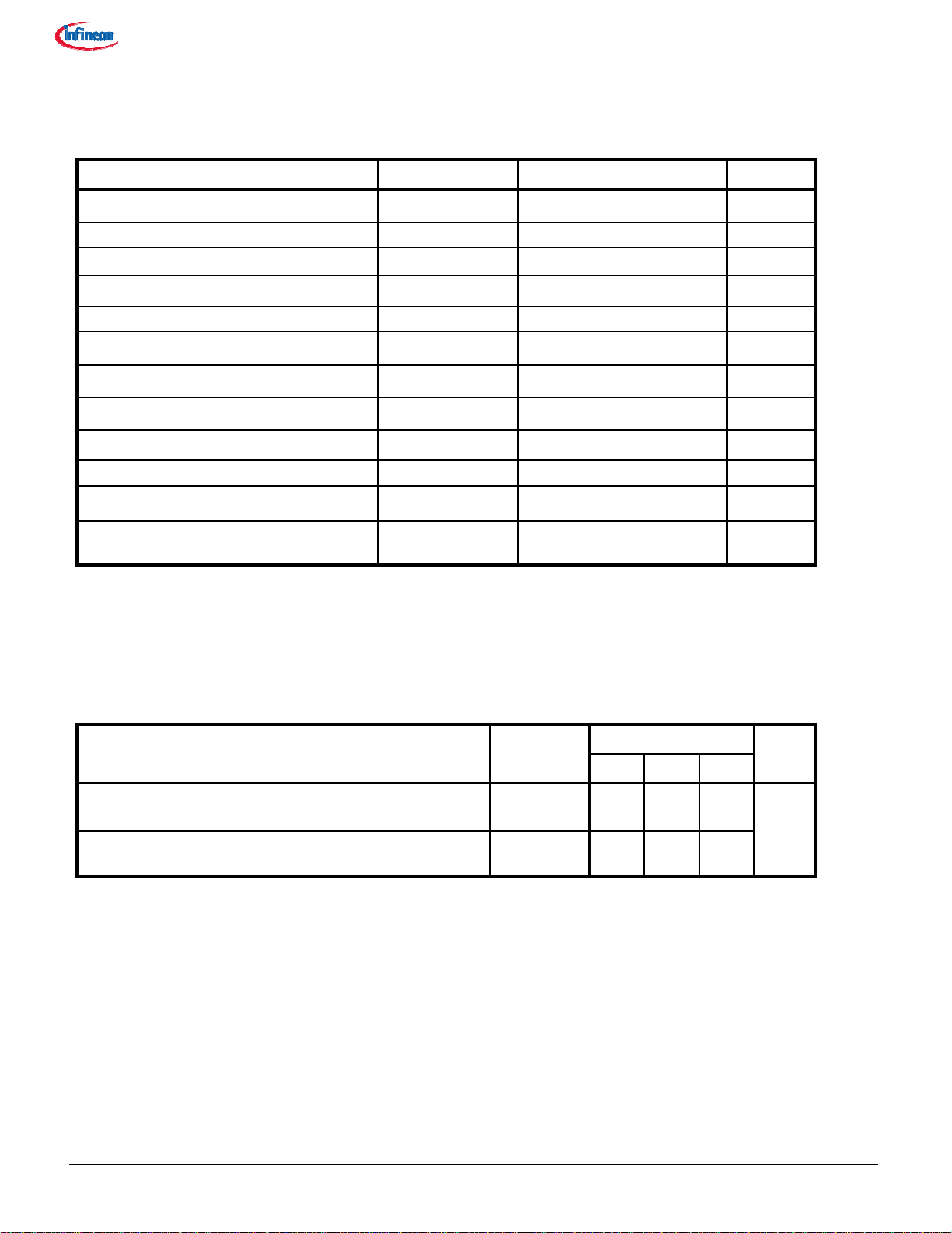
Electrical Specification Table
Absolute Maximum Ratings (Ta = 25°C)
Item Symbol Rating Units
Frequency f
SW
1.2 MHz
Average output current Iout 35 A
Input voltage VIN (DC) -0.3 to +30 V
Supply voltage VCIN (DC) -0.3 to +5.5 V
High and Low side driver voltage VDRV (DC) -0.3 to +5.5 V
Switch node voltage VSWH (DC) -1 to +30 V
BOOT voltage V
SMOD# voltage V
DISB# voltage
PWM voltage
1
1
BOOT-PHASE
SMOD#
VDISB -0.3 to +5.5 V
Vpwm -0.3 to +5.5 V
(DC) -1 to +5.5 V
(DC) -0.3 to +5.5 V
Operating junction temperature Tj-opr -40 to +150 °C
Storage temperature Tstg -55 to +150 °C
Note: All rated voltages are relative to voltages on the CGND and PGND pins unless otherwise specified.
1
Latch Up class II- Level B (Jedec 78). Please refer to Quality Report for details.
Thermal Characteristics
Parameter Symbol
Thermal resistance, junction-soldering point
Thermal resistance, junction-top of package
1
junction-soldering point is referred to the VSWH bottom exposed pad.
1
Values
Unit
Min. Typ. Max.
θ
JS
5
K/W
θ
Jtop
20
Data Sheet
Page 5 of 20
TDA21211

Recommended Operating Conditions and Electrical Characteristics (VCIN = 5V, Ta = 25°C)
Parameter Symbol Min Typ Max Units Test Conditions
Input Voltage VIN 5 25
Driving Voltage VDRV 5
Bias Supply Voltage VCIN 4.5 5 5.5
UVLO Rising V
UVLO Falling V
Driver Current
UVLO_R
UVLO_F
I
VDRV_300kHz
I
VDRV_PWML
I
VCIN_PWML
2.9 3.5 3.9
2.5 3.1 3.3
10 mA
25 µA
250 µA
IC Current (Control)
370 µA
270 µA
IC quiescent
I
VCIN_O
I
CIN+IDRV
Logic Inputs and Thresholds
V
VCIN rising
VCIN falling
DISB# = 5V, f
DISB# = 5V, PWM = 0V
DISB# = 5V, PWM = 0V
SMOD# = Open
DISB# = 5V, PWM = Open
SMOD# = Open
DISB# = 0V
= 300kHz
SW
Input low
Input high
DISB#
Sink Current
Input low
Input high
Open Voltage
SMOD#
Sink Current
Input low
Input high
Input resistance
PWM
Open Voltage
Tri-state Shutdown Window
Dynamic Characteristic
Three State to GL/GH rising
propagation delay
GL/GH Three State Shutdown
Hold-Off time,
GH Turn-on propagation delay
V
DISB_L
V
DISB_H
I
DISB
V
SMOD#_L
V
SMOD#_H
V
SMOD#_O
I
SMOD#
V
PWM_L
V
PWM_H
R
IN-PWM
V
PWM_O
V
PWM_S
T_pts
T_tsshd
T_pdhu
0.7 1.1 1.3 V
V
1.9 2.1 2.4
2 µA V
0.7 1.1 1.3 V
1.9 2.1 2.4 V
V
3.0
-8 µA V
0.7 V
V
2.4
6.5 9.5 12.5 kΩ V
1.5 V
V
1.2 1.9
15
240
15
DISB
V
DISB
DISB
SMOD#
SMOD#
SMOD#
PWM
V
PWM
PWM
PWM_O
falling
rising
= 1V
falling
rising
= 1V
falling
rising
= 1V
T_pdlu
T_pdhl
T_pdll
T_pdl_DISB
T_pdh_DISB
GH Turn-off propagation delay
GL Turn-on propagation delay
GL Turn-off propagation delay
DISB#Turn-off propogation
delay falling
DISB#Turn-on propogation
delay rising
1
Unless otherwise specified, VCIN=VDRV
Data Sheet
20
20
10
20
20
Page 6 of 20
ns
GH, GL unloaded.
TDA21211

Typical Application
+ 3.3 V
VDD
VID7
VID6
VID5
VID4
VID3
VID2
VID1
VID0
PSI#
OUTEN
VR_READY
FAULT1
FAULT2
FAULT3
VIN_SEN
PX3560
SEN1N
SEN1P
SEN2N
SEN2P
SEN3N
PWM1
PWM1
ISEN1N
ISEN1P
PWM2
ISEN2N
ISEN2P
PWM2
PWM3
ISEN3N
ISEN3P
PWM4
ISEN4N
ISEN4P
PWM5
PWM3
ISEN5N
V
IN
+12 V
C
boot
BOOT
VIN
V
CIN
TDA21211
V
DRV
PWM
C
boot
BOOT
VIN
V
CIN
TDA21211
V
DRV
PWM
C
boot
BOOT
VIN
V
CIN
TDA21211
V
DRV
PWM
CGND
CGND
CGND
R
boot
PHASE
R
boot
PHASE
R
boot
PHASE
VSWH
PGND
VSWH
PGND
VSWH
PGND
Rb
Rb
Rb
L
Cb
L
Cb
L
Cb
V
CIN
+
Data Sheet
SEN3P
SDA
SCL
SADDR_M
ISEN5P
PWM6
ISEN6N
ISEN6P
C
boot
BOOT
VIN
V
CIN
TDA21211
V
DRV
R
boot
PHASE
VSWH
Rb
L
Cb
SADDR_L
VD25
PWM4
SEN4N
PWM
CGND
PGND
GND
SEN4P
VSENP
VSENP
VSENN
V
OUT
C
OUT
VSENN
Figure 3. Four Phases Voltage Regulator Typical Application (Simplified Schematic)
Page 7 of 20
TDA21211

Theory of Operation
The TDA21211 incorporates a high performance gate driver, one high side power MOSFET and one low-side power
MOSFET in a single 40 lead QFN package. The advantages of this arrangement are found in the areas of increased
performance, increased efficiency and lower overall package and layout inductance.This module is ideal for use in
Synchronous Buck Regulators either as a stand-alone power stage that can deliver up to 35A or with an interleaved
approach for higher current loads.
The power MOSFETs are tailored for this device. The gate driver is an extremely robust high-performance driver rated
at the switching node for DC voltages ranging from -1V to +30V. The closely coupled driver and MOSFETs enable
efficiency improvements that are hard to match using discrete components. The power density for transmitted power
2
V
UVLO_F
area.
Enable
V
UVLO_R
V
CIN
of this approach is approximately 30W within a 36mm
Driver Characteristics
The gate driver of the TDA21211 has 2 voltage inputs, VCIN and VDRV. VCIN is the 5V bias supply for the driver.
VDRV is also 5V and is used to drive the High and Low Side MOSFETs. Ceramic capacitors should be placed very
close to these input voltage pins to decouple the sensitive control circuitry from a noisy environment.
The MOSFETs selected for this application are optimized for 5V gate drive, thus giving the end user optimized high
load as well as light load efficiency. The reference for the power circuitry including the driver output stage is PGND
and the reference for the gate driver control circuit (VCIN) is CGND.
Referring to the Block Diagram, Figure 2 VCIN is internally connected to the UVLO circuit and for VCIN voltages less
than required for proper circuit operation will provide shut-down. VDRV supplies both, the floating high side drive and
the low-side drive circuits. An active boot circuit for the high side gate drive is also included. A second UVLO circuitry,
sensing the BOOT voltage level, is implemented to prevent false GH turn on during insufficient power supply level
condition (BOOT Cap charging/discharging sequence). During undervoltage both GH and GL are driven low actively;
further passive pull down (500k Ohm) is placed on each gate.
Note: output signal from UVLO unit.
UVLO Output
Logic Level
“H”
“L”
Shutdown
Data Sheet
Page 8 of 20
TDA21211

Inputs to the internal control circuit are PWM, DISB# and SMOD#:
The PWM is the control input to the IC from an external PWM controller and is compatible with 3.3V and 5V logic.
The PWM input has three-state functionality. When the voltage remains in the specified PWM-shutdown-window for at
least the PWM-shutdown-holdoff time T_tsshd, the operation will be suspended by keeping both MOSFET gate outputs
low. Once left open, the pin is internally fixed to V
= 1.5 V level
PWM_O
PWM Driver Output
L GL=H, GH = L
H GL=L, GH = H
Open GL=L, GH = L
The DISB# is an active low signal. When DISB# is pulled low, the power stage is disabled.
DISB# Driver Output
L Shutdown Æ GL, GH = L
H EnableÆ GL, GH = “Active”
Open Shutdown Æ GL, GH = L
The SMOD# feature is provided to disable the low-side MOSFET during active operation. When synchronized with the
PWM signal (as shown in Figure 7), SMOD# is intended to improve light load efficiency by saving the gate charge loss
of the low-side MOSFET. Once left open, the pin is internally fixed to V
SMOD#_O
= 3 V level.
SMOD# GL Status
L L
H Enable Æ GL= “Active”
Open Enable Æ GL= “Active”
The TDA21211 driver includes gate drive functionality to protect against shoot through. In order to protect the power
stage from overlap, both HS and LS MOSFETs being on at the same time, the adaptive control circuitry monitors the
voltage at the “VSWH” pin. When the PWM signal goes low, HS, the High-side MOSFET will begin to turn off, after the
propagation delay (T_pdlu). Once the “VSWH” pin falls below 1V, LS, the Low-side MOSFET is gated on after the
predefined delay time, (T_pdhl). Additionally, the gate to source voltage of the HS-MOSFET is also monitored. When
VGS(HS) is discharged below 1V, a threshold known to turn HS off, a secondary delay is initiated, (T_pdhl), which
results in LS being gated “ON” irregardless of the state of the “VSWH” pin.This way it will be ensured that the converter
can sink current efficiently and the bootstrap capacitor will be refreshed appropriately during each switching cycle. See
Figure 5 for more detail.
GH and GL are monitoring pins to check the internal gate drive signals.
Data Sheet
Page 9 of 20
TDA21211

V
IN
C
IN
4x10u F
(+ 5 ÷ 24 v)
VIN
VSWH
PGND
C
BOOT
0.1 ÷ 1u F
R
BOOT
0 ÷ 5 Ω
VIN
NC
8910
11
12
13
14
15
16
17
18
VIN
PHASE
7
GH
CGND
6
VSWH
+ 5 v
VDRV
BOOT
CGND
VCIN
1u F
1u F
12345
CGND
CGND
SMOD
40
39
38
37
36
35
34
33
CGND
PWM
DISB#
NC
CGND
GL
VSWH
19
20
Signal GND Power GND
22 23 24 25 26 27
21
Figure 4. Pin interconnection outline (Transparent Top View)
NOTE: R
value is related to the input voltage level.
BOOT
Pin PHASE is internally connected to VSWH node.
32
31
28
PGND
30
29
L
V
OUT
VSWH
Data Sheet
Page 10 of 20
TDA21211

V
V
V
V
V
Gate Driver Timing Diagrams
PWM_H
PWM_L
PWM
T_pdll
GL
T_pdhl
PWM_H
PWM_L
T_tsshd
T_pts
GH
SWH
1 V
T_pdhu
T_tsshd
T_pdlu
1 V
T_pts
Note: VSWH during entering/exit to tri-
state behaves accordingly to inductor
current.
Figure 5: Adaptive Gate Driver Timing Diagram
Data Sheet
Page 11 of 20
TDA21211

)
V
V
DISBL#
DISB_H
DISB_L
GH/GL
SMOD
T_pdl(DISB
Figure 6: Disable Timing Diagram
T_pdh(DISB)
SMOD disabled
SMOD active
PWM
GL
T_pdlu
T_pdlu
CCM
DCM
T_pdlu
CCM
Figure 7 SMOD# Timing Diagram
Data Sheet
Page 12 of 20
TDA21211

×
Test Circuit
V
V
IN
IN
V
V
CIN
CIN
V
V
DRV
DRV
PWM
PWM
I
I
IN
IN
I
I
CIN
CIN
I
I
DRV
DRV
A
A
C
V
V
A
A
C
C
CIN
V
V
A
A
V
V
VDRV
VDRV
PWM
PWM
CIN
C
C
DRV
DRV
VIN
VIN
BOOT
BOOT
C
IN
IN
C
C
BOOT
BOOT
PHASE
PHASE
VSWH
VSWH
PGND
PGND
300n H
300n H
R
R
b
b
L
L
C
C
V
V
OUT
OUT
I
I
OUT
OUT
b
b
C
C
OUT
OUT
PX3560
PX3560
V
V
V
V
I
I
SENN
SENN
I
I
SENP
SENP
SENP
SENP
SENN
SENN
VCIN
VCIN
DISBL#
DISBL#
SMOD#
SMOD#
CGND
CGND
TDA21211
TDA21211
Figure 8. Test Circuit
P
OUT
Efficiency =
P
IN
IVIVIVP
ININCINCINDRVDRVIN
Page 13 of 20
TDA21211
Data Sheet
IVP ×=
OUTOUTOUT
PPP −=
OUTINLOSS
+×+×=

Performance Curves – Typical Data
Operating conditions (unless otherwise specified): VIN= +12V, V
59P9081N01, DCR (typ) =0.43m Ω) T
=25° C, load line=0mΩ, airflow=100 LFM, no heatsink. Power Efficiency and Power Loss data
A
CIN=VDRV
= +5V, V
=1.1 V, F=362k Hz, 300nH inductor (VITEC-
OUT
reported herein includes TDA21211 and inductor losses but no other system losses (unless otherwise specified).
94
92
90
88
86
1. 6 V
1. 5 V
1. 2 V
1. 0 V
0.8V
7
0.8V
6
5
1. 0 V
1. 2 V
1. 5 V
1. 6 V
4
3
Efficiency (%)
Power Loss (W)
84
82
80
0 5 10 15 20 25 30
Output Current (A)
Figure 9. Efficiency vs. VOUT
2
1
0
0 5 10 15 20 25 30
Output Current (A)
Figure 10. Power Loss vs. VOUT
94
92
90
88
86
Efficien cy (%)
84
82
80
0 5 10 15 20 25 30
O utput Current (A)
Figure 11. Efficiency vs. Switching Frequency
296Khz
362Khz
407Khz
465Khz
592Khz
7
6
59 2Khz
4 65Khz
4 07Khz
362Khz
296Khz
5
4
3
Power Loss (W)
2
1
0
0 5 10 15 20 25 30
Output Current (A)
Figure 12. Power Loss vs. Switching Frequency
Data Sheet
Page 14 of 20
TDA21211

94
92
90
88
86
Efficiency (%)
84
82
80
0 5 10 15 20 25 30
Output Current (A)
Figure 13. Efficiency vs. VIN
10 V
12 V
14 V
16 V
18 V
20V
7
20V
6
5
18 V
16 V
14 V
12 V
10 V
4
3
Power Loss (W)
2
1
0
0 5 10 15 20 25 30
O u tp u t Current (A)
Figure 14. Power Loss vs. VIN
94
92
90
88
86
Effici ency (%)
84
82
80
0 5 10 15 20 25 30
Output Current (A)
25C
65C
85C
10 5C
7
10 5C
6
85C
65C
25C
5
4
3
Power Loss (W)
2
1
0
0 5 10 15 20 25 30
O u tpu t Current (A)
Data Sheet
Figure 15. Efficiency vs. T
CASE
Page 15 of 20
Figure 16. Power Loss vs. T
TDA21211
CASE

V
V
V
7
in=12V
VCIN=VDRV=5V
6
Vout=1.3V
F=600kHz
5
L=510nH
T= 25° C
4
3
Power Loss (W)
2
1
0
0 5 10 15 20 25 30
Output Current (A)
Figure 17.
(inductor losses not included)
Power Loss vs. Iout
1,20
in=12V
1,15
1,10
1,05
VCIN=VDRV=5V
Vout=1.3V
Iout=25A
L=510nH
T= 25° C
1,00
0,95
0,90
0,85
300 400 500 600 700 800 900 1000
Figure 18.
Switching Frequency (kHz)
Normalized Power Loss @ Iout=25 A
(inductor losses not included)
(mA)
CIN
+ I
DRV
I
35
30
25
20
15
10
in=12V
VCIN=VDRV=5V
Vout=1.3V
Iout=25A
L=510nH
T= 25° C
5
0
100 200 300 400 500 600 700 800 900 1000
Switching Frequency (kHz)
Figure 19.
Data Sheet
Power Supply Current (IDRV + ICIN) vs. Fsw
Page 16 of 20
TDA21211

Package Outline
PIN#1 IDENT
Data Sheet
Page 17 of 20
TDA21211

Figure 20: Footprint and Solder Stencil Recommendation
Data Sheet
Page 18 of 20
TDA21211

PCB Layout Example.
Figure 21 Single Phase DrMOS typical Application Circuit
Data Sheet
Figure 22 Single Phase DrMOS PCB Layout Example (Top Side View)
(for DrMOS Design support a customer PCB layout guide is available upon request)
Page 19 of 20
TDA21211

For questions on technology, delivery and prices please contact the Infineon Technologies Offices in Germany or the
Infineon Technologies Companies and Representatives worldwide: see the address list on the last page or our webpage
at
http://www.infineon.com/DCDC
CoreControlTM, OptiMOS™ and OptiMOS II™ are trademarks of Infineon Technologies AG.
We listen to Your Comments
Any information within this document that you feel is wrong, unclear or missing at all?
Your feedback will help us to continously improve the quality of this document.
Edition 2004-11-10
Published by Infineon Technologies AG,
St.-Martin-Strasse 53,
D-81541 München
© Infineon Technologies AG 2004.
All Rights Reserved.
Attention please!
The information herein is given to describe certain components and shall not be considered as warranted characteristics.
Terms of delivery and rights to technical change reserved.
We hereby disclaim any and all warranties, including but not limited to warranties of non-infringement, regarding circuits, descriptions and charts stated herein.
Infineon Technologies is an approved CECC manufacturer.
Information
For further information on technology, delivery terms and conditions and prices please contact your nearest Infineon Technologies Office in Germany or our Infineon
Technologies Representatives worldwide (see address list).
Warnings
Due to technical requirements components may contain dangerous substances. For information on the types in question please contact your nearest Infineon Technologies
Office.
Infineon Technologies Components may only be used in life-support devices or systems with the express written approval of Infineon Technologies, if a failure of such
components can reasonably be expected to cause the failure of that life-support device or system, or to affect the safety or effectiveness of that device or system. Life support
devices or systems are intended to be implanted in the human body, or to support and/or maintain and sustain and/or protect human life. If they fail, it is reasonable to
assume that the health of the user or other persons may be endangered.
Data Sheet
Page 20 of 20
TDA21211
 Loading...