现货库存、技术资料、百科信息、热点资讯,精彩尽在鼎好!
CoreControl
TM
Data Sheet TDA21106
High speed Driver with bootstrapping for
dual Power MOSFETs
Features
• Fast rise and fall times for frequencies up to 2 MHz
• Capable of sinking more than 4A peak currents for lowest switching losses
• Charges High Side MOSFET gate drive voltage from 6 to 12V according to PVCC
setting; Low Side MOSFET at 12 V.
• Adjustable High Side MOSFET gate drive voltage via PVCC pin for optimizing ON
losses and gate drive losses
• Integrates the bootstrap diode for reducing the part count
• Prevents from cross-conducting by adaptive gate drive control
• High voltage rating on Phase node
• Supports shut-down mode for very low quiescent current through three-state input
• Compatible to standard PWM controller ICs (Intersil, Analog Devices)
• Floating High Side MOSFET drive
• Footprint compatible to TDA21101G and HIP6601B
• Ideal for multi-phase Desktop CPU supplies on motherboards and VRM´s
Type Package Marking Ordering Code
TDA21106 P-DSO-8 21106 Q67042-S4223
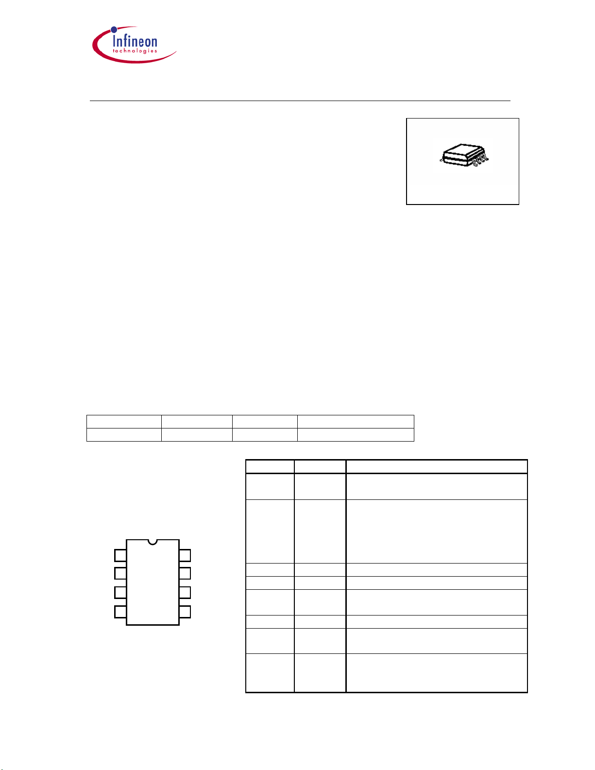
P-DSO-8
Number Name Description
Pinout
1 GATEHS Gate drive output for the N-Channel
High side MOSFET
2 BOOT Floating bootstrap pin. To be
Top View
connected to the external bootstrap
capacitor to generate the gate drive
voltage for the high side N-Channel
GATE
BOOT 2 7 P
PWM 3 6 V
GND 4 5 GATE
1 8 PHASE
HS
VCC
CC
MOSFET
3 PWM Input for the PWM controller signal
4 GND Ground
LS
5 GATELS Gate drive output for the N-Channel
Low Side MOSFET
6 VCC Supply voltage
7 PVCC Input to adjust the High Side gate
drive
8 PHASE To be connected to the junction of
the High Side and the Low Side
MOSFET
Rev 2.0 Page 1 Apr, 2004

CoreControl
General Description
The dual high speed driver is designed to drive a wide range of N-Channel low side
and N-Channel high side MOSFETs with varying gate charges. It has a small
propagation delay from input to output, short rise and fall times and the same pin
configuration to be compatible to TDA21101G and HIP6601B. In addition it provides
protection features as well as a three-state mode for efficiency reasons. The high
breakdown voltage makes it suitable for mobile applications.
Target application
The dual high speed driver is designed to work well in half-bridge type circuits where
dual N-Channel MOSFETs are utilized. A circuit designer can fully take advantage of
the driver´s capabilities in high-efficiency, high-density synchronous DC/DC
converters that operate at high switching frequencies, e.g. in multi-phase converters
for CPU supplies on motherboards and VRM´s but also in motor drive and class-D
amplifier type applications.
Absolute Maximum Ratings
At Tj = 25 °C, unless otherwise specified
TM
Data Sheet TDA21106
Value Parameter Symbol
Min. Max.
Unit
Voltage supplied to ‘VCC’ pin; DC V
Voltage supplied to ‘PVCC’ pin; DC V
Voltage supplied to ‘PWM’ pin V
Voltage supplied to ‘BOOT’ pin referenced to ‘PHASE’ V
Voltage supplied to ‘BOOT’ pin referenced to ‘GND’ V
Voltage rating at ‘PHASE’ pin, DC V
Voltage rating at ‘PHASE’ pin, t
pulse_max
= 500ns
-0.3 25
VCC
-0.3 25
PVCC
-0.3 5,5
PWM
–
BOOT
V
PHASE
BOOT
PHASE
V
PHASE
-0,3 25
-0,3 45
-1 25
-20 30
V
Max Duty Cycle = 2%
Voltage supplied to GATEHS pin referenced to ‘PHASE’
T
pulse_max
< 100ns, Energy < 2uJ
Voltage supplied to GATELS pin referenced to ‘GND’
T
pulse_max
< 100ns, Energy < 2uJ
V
GATEHS
V
GATELS
Junction temperature TJ -25 150
-3.5 V
+0.3
-5 V
BOOT
VCC
+0.3
°C
Storage temperature TS -55 150
ESD Rating; Human Body Model 4 KV
IEC climatic category; DIN EN 60068-1 55/150/56 -
Rev 2.0 Page 2 Apr, 2004

CoreControl
Thermal Characteristic
Thermal resistance, junction-soldering point 95
Thermal resistance, junction-ambient 125
Operating Conditions
At Tj = 25 °C, unless otherwise specified
Parameter Symbol Conditions
TM
Data Sheet TDA21106
Values Parameter Symbol
Min. Typ. Max.
Values
Min. Typ. Max.
Unit
K/W
Unit
Voltage supplied to
‘VCC’ pins
Voltage supplied to
‘PVCC’ pins
Input signal transition
V
10.8 13.2 V
VCC
V
6 13.2 V
PVCC
f 0.1 2 MHz
frequency
Power dissipation P
TA = 25 °C, TJ = 125 °C 0.8 W
TOT
Junction temperature TJ -25 150 °C
Electrical Characteristic
At Tj = 25 °C, unless otherwise specified
Parameter Symbol Conditions
Values
Unit
Min. Typ. Max.
Supply Characteristic
Quiescent current I
PVCC+IVCCQ
VCC supply current I
PVCC supply current I
1.8 V ≤ V
f =1 MHz,
VCC
V
= V
PVCC
No load
f =1 MHz,
PVCC
V
= V
PVCC
PWM
VCC
VCC
≤ 3.0 V
= 12 V
= 12 V
1,3. 3
5
8
6
8.5
mA
No load
Under-voltage
V
rising threshold 9.7 10.1 10.5
VCC
V
lockout
Under-voltage
V
falling threshold 7.3 7.6 8.0
VCC
lockout
Input Characteristic
Current in ‘PWM’ pin I
Current in ‘PWM’ pin I
Shut down window V
Shut down hold-off
V
PWM_L
V
PWM_H
SHUT
t_
1.6 V ≤ V
IN_SHUT
t_
= 0.4 V -80 -115 -150
_PWM
= 4.5 V 120 180 250
_PWM
> 300 ns 1.7 3.1 V
SHUT
PWM
≤ 3.2 V
100 190 300 ns
µA
time
PWM pin open V
PWM Low level V
PWM High level V
Pulse width High
Side
Rev 2.0 Page 3 Apr, 2004
1.8 2.0 2.2
PWM_O
1.4
PWM_L
3.7
PWM_H
t_P = Pulse width on PWM
40 ns
pin
V
 Loading...