

现货库存、技术资料、百科信息、热点资讯,精彩尽在鼎好!
CoreControl
TM
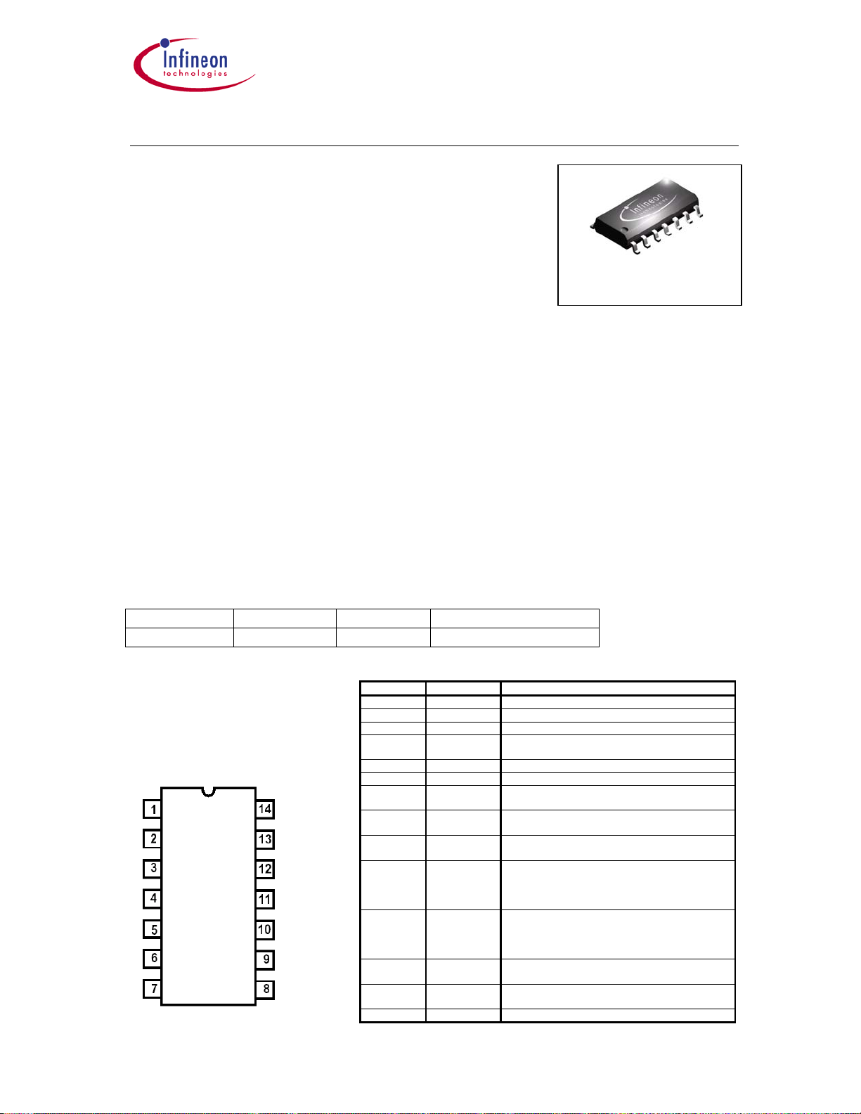
Data Sheet TDA21102
High speed Driver with bootstrapping for
dual Power MOSFETs
Features
• Fast rise and fall times for frequencies up to 2 MHz
• Capable of sinking more than 4 A peak current for lowest switching losses
• Charges the High Side and Low Side MOSFET´s gate to 6..12 V according to
PVCC setting.
• Adjustable High Side and Low Side MOSFET gate drive voltage via PVCC pin for
optimizing ON losses and gate drive losses
• Integrates the bootstrap diode for reducing the part count
• Prevents from cross-conducting by adaptive gate drive control
• High voltage rating on Phase node
• Supports shut-down mode for very low quiescent current through three-state input
• Compatible to standard PWM controller ICs (Intersil, Analog Devices)
• Floating High Side MOSFET drive
• Ideal for multi-phase Desktop CPU supplies on motherboards and VRM´s
Type Package Marking Ordering Code
TDA21102 P-DSO-14-3 21102 Q67042-S4244
Pinout
LS1
LS2
PWM1 VCC
PWM2 PHASE1
GND GATGATE
GATE
PVCC BOOT2
PGND GATE
GATE
Top View
HS1
BOOT1
HS2
PHASE2
Rev. 1.0 Page 1 Dec 19, 2003
Number Name Description
1 PWM1 Input for the PWM1 controller signal
2 PWM2 Input for the PWM2 controller signal
3 GND Ground
4 GATE
5 PVCC Input to adjust the High Side gate drive
6 PGND Power ground return for the Low Side Drivers
7 GATE
8 PHASE2 To be connected to the junction of the High
9 GATE
10 BOOT2 Floating bootstrap pin. To be connected to the
11 BOOT1 Floating bootstrap pin. To be connected to the
12 GATE
13 PHASE1 To be connected to the junction of the High
14 VCC Supply Voltage
P-DSO-14-3
P-DSO-8-7
Gate drive output for the N-Channel Low Side
LS1
LS2
HS2
HS1
MOSFET 1.
Gate drive output for the N-Channel Low Side
MOSFET 2.
Side and the Low Side MOSFET 2
Gate drive output for the N-Channel High Side
MOSFET 2.
external bootstrap capacitor to generate the
gate drive voltage for the High Side N-Channel
MOSFET 2.
external bootstrap capacitor to generate the
gate drive voltage for the High Side N-Channel
MOSFET 1.
Gate drive output for the N-Channel High Side
MOSFET 1.
Side and the Low Side MOSFET 1
CoreControl
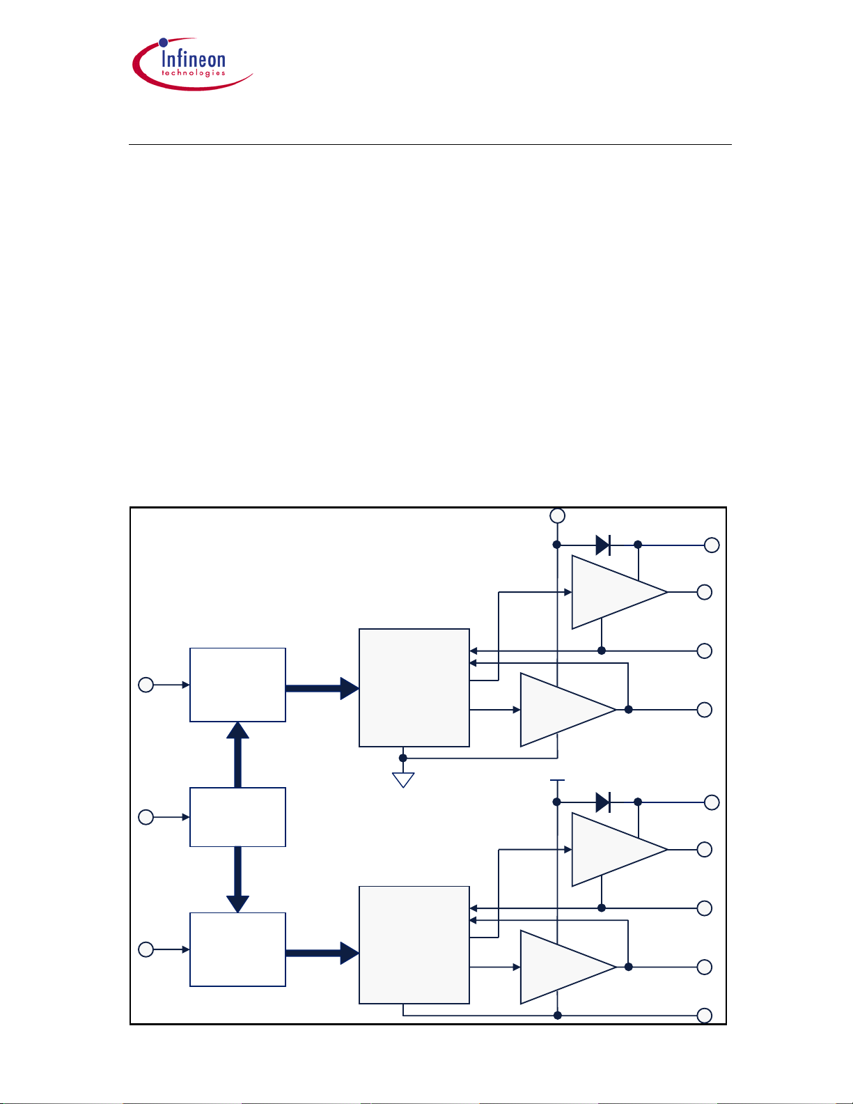
General Description
The dual high speed driver is designed to drive a wide range of N-Channel low side
and N-Channel high side MOSFETs with varying gate charges. It has a small
propagation delay from input to output, short rise and fall times and the same pin
configuration as the HIP6602B. In addition it provides several protection features as
well as a shut down mode for efficiency reasons. The high breakdown voltage makes
it suitable for mobile applications.
Target application
The dual high speed driver is designed to work well in half-bridge type circuits where
dual N-Channel MOSFETs are utilized. A circuit designer can fully take advantage of
the driver´s capabilities in high-efficiency, high-density synchronous DC/DC
converters that operate at high switching frequencies, e.g. in multi-phase converters
for CPU supplies on motherboards and VRM´s but also in motor drive and class-D
amplifier type applications.
Block Diagram
TM
Data Sheet TDA21102
PWM
VCC
PWM
Control
Logic
Bias
Control
Logic
Shoot
Through
Protection
GND
Shoot
Through
Protection
PVCC
LS
Driver
PVCC
LS
Driver
HS
Driver
HS
Driver
BOOT
GATE
PHASE
GATE
BOOT
GATE
PHASE
GATE
HS
LS
HS
LS
GND
Rev. 1.0 Page 2 Dec 19, 2003
CoreControl
Absolute Maximum Ratings
At Tj = 25 °C, unless otherwise specified
TM
Data Sheet TDA21102
Value Parameter Symbol
Min. Max.
Unit
Voltage supplied to ‘VCC’ pin V
Voltage supplied to ‘PVCC’ pin V
Voltage supplied to ‘PWM’ pin V
Voltage supplied to ‘BOOT’ pin referenced to ‘PHASE’ V
Voltage rating at ‘PHASE’ pin, DC V
Voltage rating at ‘PHASE’ pin, t
pulse_max
=500ns
-0.3 25
VCC
-0.3 25
PVCC
-0.3 5.5
PWM
–
BOOT
V
PHASE
PHASE
-0.3 25
-1 25
-20 30
V
Max Duty Cycle = 2%
Junction temperature TJ -25 150
°C
Storage temperature TS -55 150
ESD Rating; Human Body Model 4 kV
IEC climatic category; DIN EN 60068-1 55/150/56 -
Thermal Characteristic
Values UnitParameter Symbol
Min. Typ. Max.
Thermal resistance, junction-case Rth-JC 44,7
K/W
Thermal resistance, junction-ambient Rth-JA 116,2
Electrical Characteristic
At Tj = 25 °C, unless otherwise specified
Parameter Symbol Conditions
Values
Unit
Min. Typ. Max.
Supply Characteristic
Bias supply current I
Quiescent current I
Power supply current I
f = 1 MHz,
VCC
VCCQ
f = 1 MHz,
PVCC
1.8 V ≤ V
Under-voltage lockout V
Under-voltage lockout V
NO LOAD
V
PVCC
= V
VCC
PWM
= 12 V
≤ 3.0 V
NO LOAD
V
= V
PVCC
rising threshold 9.7 10.1 10.5 V
VCC
falling threshold 7.3 7.6 8.0 V
VCC
VCC
= 12 V
0.95 1.65
0.75 3
26
mA
Input Characteristic
Current in ‘PWM’ pin I
Current in ‘PWM’ pin I
Shut down window V
Shut down hold-off
V
PWM_L
V
PWM_H
SHUT
t_
1.7 V ≤ V
IN_SHUT
t_
= 0.4 V -80 115 -150
_PWM
= 4.5 V 120 180 250
_PWM
> 320 ns 1.7 3.1 V
SHUT
PWM
≤ 3.1 V
100 230 350 ns
µA
time
PWM pin open V
1.8 2.0 2.2
PWM_O
Rev. 1.0 Page 3 Dec 19, 2003

S
S
CoreControl
PWM Low level
threshold (falling)
PWM High level
threshold (rising)
Pulse Width High
Side
At Tj = 25 °C, unless otherwise specified
Dynamic Characteristic
Turn-on propagation
Delay High Side*
Turn-off propagation
delay High Side
Rise time High Side t
Fall time High Side t
Turn-on propagation
Delay Low Side
Turn-off propagation
delay Low Side
Rise time Low Side t
Fall time Low Side t
Measurement Timing diagram
PWM @
TM
Data Sheet TDA21102
V
V
1.45 1.55
PWM_L
PWM_H
3.45 3.6
t
_p
t
d(ON)_HS
= Pulse with on PWM pin 40 ns
27 35
t
d(OFF)_HS
16 21
20 25
r_HS
11 20
f_HS
t
d(ON)_LS
P
PVCC
20 23
C
= V
VCC
= 3000 pF
ISS
= 12 V
t
d(OFF)_LS
13 20
22 25
r_LS
f_LS
13 20
PWM @
V
ns
T
d(ON)_H
T
d(Off)_H
PWM
GATEHS @ 90%
T
d(Off)_LS
GATEHS @ 10%
T
T
r_HS
f_HS
T
d(On)_LS
GATE
H
PHASE @ 5V
PHASE
GATELS @ 90%
GATE
@ 5V
LS
GATE
L
GATELS @ 10%
T
f_LS
Rev. 1.0 Page 4 Dec 19, 2003
T
r_LS

CoreControl
Operating Conditions
At Tj = 25 °C, unless otherwise specified
Parameter Symbol Conditions
TM
Data Sheet TDA21102
Values
Min. Typ. Max.
Unit
Voltage supplied to
‘VCC’ pin
Voltage supplied to
‘PVCC’ pin
Input signal transition
V
10.8 13.2 V
VCC
V
6 13.2 V
PVCC
f 0.1 2 MHz
frequency
Power dissipation P
TA = 25 °C, TJ = 125 °C 0.9 W
TOT
Junction temperature TJ -25 150 °C
At Tj = 25 °C, unless otherwise specified
Parameter Conditions
Values
Unit
Min. Typ. Max.
Output Characteristic High Side (HS) and Low Side (LS), ensured by design
Output
HS; Source P
Resistance
HS; Sink P
LS; Source P
LS; Sink P
Peak output-
current
Rev. 1.0 Page 5 Dec 19, 2003
HS; Source 4
HS; Sink 4
LS; Source 4
LS; Sink
t_
t_
D
= V
P
P_HS
P_LS
_HS
PVCC
PVCC
PVCC
PVCC
PVCC
I
_HS_SRC
I
_HS_SRC
VCC
= V
VCC
= V
VCC
= V
= V
VCC
/ Pulse < 20 ns
/ Pulse < 40 ns
< 2%, D
= 12 V
1.2
= 2 A
= 12 V 1 1.5
= 12 V
1
= 2 A
= 12 V 1 1.3
VCC
= 12 V
_LS
< 4%
4
Ω
Ω
Ω
Ω
A

CoreControl
Package Drawing P-DSO-14-3
TM
Data Sheet TDA21102
Layout Footprints
e A L B
1,27 mm 5,69 mm 1,31 mm 0,65 mm
Rev. 1.0 Page 6 Dec 19, 2003

CoreControl
Published by
Infineon Technologies AG,
Bereichs Kommunikation
St.-Martin-Strasse 53,
D-81541 München
Infineon Technologies AG 1999
All Rights Reserved.
Attention please!
The information herein is given to describe certain components and shall not be considered as warranted
characteristics.
Terms of delivery and rights to technical change reserved.
We hereby disclaim any and all warranties, including but not limited to warranties of non-infringement,
regarding circuits, descriptions and charts stated herein.
Infineon Technologies is an approved CECC manufacturer.
Information
For further information on technology, delivery terms and conditions and prices please contact your
nearest Infineon Technologies Office in Germany or our Infineon Technologies Representatives
worldwide (see address list).
Warnings
Due to technical requirements components may contain dangerous substances.
For information on the types in question please contact your nearest Infineon Technologies Office.
Infineon Technologies Components may only be used in life-support devices or systems with the
express written approval of Infineon Technologies, if a failure of such components can reasonably be
expected to cause the failure of that life-support device or system, or to affect the safety or
effectiveness of that device or system Life support devices or systems are intended to be implanted in
the human body, or to support and/or maintain and sustain and/or protect human life. If they fail, it is
reasonable to assume that the health of the user or other persons may be endangered.
TM
Data Sheet TDA21102
Rev. 1.0 Page 7 Dec 19, 2003
 Loading...