Infineon TDA16847G, TDA16847, TDA16846G, TDA16846 Datasheet

ICs for Consumer Electronics
Controller for Switch Mode Pow er Supplies Supporting Low Power
Standby and Power Factor Correction
TDA 16846/TDA 16847
Data Sheet 2000-01-14

TDA 16846/TDA 16847
Revision History: Current Version: 2000-01-14
Previous Version: 1999-07-05
Page
(in previous
Version)
Page
(in current
Version)
Subjects (major changes since last revision)
3 3, 28 P-DSO package added
Edition 01.00
Published by Infineon Technologies AG i. Gr.,
St.-Martin-Strasse 53
D-81541 München
© Infineon Technologies AG 2000
All Rights Reserved.
Attention plea se !
The informatio n herein is given to describe certain compon ents and shall not be considered as warranted characterist ics.
Terms of delivery and rights to technical change reserved.
We hereby disclaim any and all warranties, including but not limited to warranties of non-infringement, regarding circuits, descriptions and
charts stated herein.
Infineon Technologiesis an appro v ed CECC manufacturer.
Information
For further information on technology, del ivery terms and conditions and prices p l ease contact your near est Infineon Technologies O ffi c e
in Germa ny or our In fineon Technologies Representati ves worldwide (see address list).
Warnings
Due to technical requirements components may contai n dangerous substances. F or information on the types in question please contact
your nearest Infineon Technologies Office.
Infineon Technologies Components may only be used in life-support devices or systems with the express written approval of Infineon T e chnologies, if a failure of such components can reasonably be expected to cause the failure of that life-support device or system, or to aff ect
the saf et y or ef f ect i v en ess of tha t device or sys tem. Life supp ort de vi ces or syst ems are in te nd ed t o be impl an t ed i n th e hu man body, or to
support a nd/or maintain and sustain and/or protect human life. If they fail, it is reas onable to assume that the health of the user or other
persons may be endangered.
Controller for Switch Mode Power Supplies
Supporting Low Power Standby and Power
TDA 16846
TDA 16847
Factor Correction
Preliminary Data Bipolar IC
1 Overview
1.1 Features
• Line Current Consumption with PFC
• Low Power Consumption
• Stable and Adjustable Standby Frequency
• Very Low Start-up Current
• Soft- Sta rt for Quiet Start-up
• Free usable Fault Comparators
• Synchronization and Fixed Frequency Facility
• Over- and Undervoltage Lockout
• Switch Off at Mains Undervoltage
• Temporary high power circuit (only TDA 16847)
• Mains Voltage Dependent Fold Back Point Correction
• Continuous Frequency Reduction with Decreasing Load
• Adjustable and Voltage Dependent Ringing Suppressi on Time
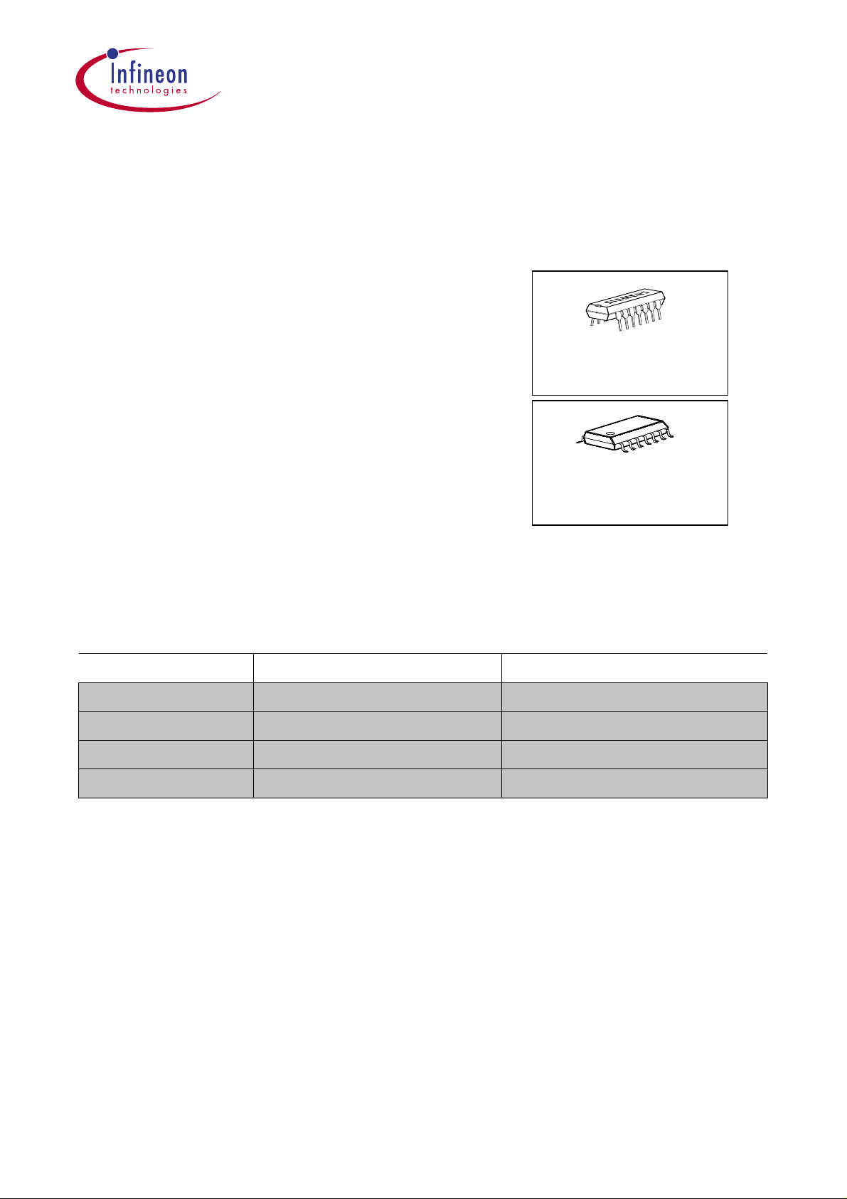
P-DIP-14-3
P-DSO-14-3
Type Ordering Code Package
TDA 16846 Q67000-A9377 P-DIP-14-3
TDA 16847 Q67000-A9378 P-DIP-14-3
TDA 16846G Q67006-A9430 P-DSO-14-3
TDA 16847G Q67006-A9412 P-DSO-14-3
1.2 Description
The TDA 16846 is optimized to control free running or fixed frequency flyback converters
with or without Power Factor Correction (Current Pump). To provide low power
consumption at light loads, this device reduces the switching frequency continuously
with load, towards an adj ust able mini mu m (e. g. 20 kHz i n sta ndby m ode) . Addition ally,
the start up current is ve ry low. To avoid switching stresses of the power devices, the
power transistor is always switched on at minimum voltage. A special circuit is
V
implemented to avo id jitter. The device has sev eral protec tion functions:
undervoltage, main s under volta ge, c urrent limit ing and 2 f ree u sabl e fa ult com par ato rs.
Regulation can be done by using the internal error amplifier or an opto coupler feedback
(additional input). The output driver is ideally suited for driving a power MOSFET, but it
can also be used for a bipolar transi stor. Fixed frequency and synchronized op eration
are also possible.
over- a nd
CC
Data Sheet 3 2000-01-14

TDA 16846
TDA 16847
The TDA 16846 is suited for TV-, VCR- sets and SAT receivers. It also can be good used
in PC monitors.
The TDA 16847 is i denti cal with TDA 16846 but has an additional power measurement
output (pin 8) which can be used for a Temporary High Power Circuit.
OTC
PCS
RZI
SRC
OCI
FC2
SYN N.C./PMO
1
2
3
4
5
6
7
Figure 1 Pin Configuration (top view)
1.3 Pin Definitions and Functions
Pin Symbol Function
1 OTC Off Time Circuit
14
13
12
11
10
9
8
AEP02647
VCC
OUT
GND
PVC
FC1
REF
2 PCS Primary Current Simulation
3 RZI Regulation and Zero Crossing Input
4 SRC Soft-Start and Regulat ion Capac itor
5 OCI Opto Coupler Input
6 FC2 Fault Comparator 2
7 SYN Synchronization Input
8 N.C./PMO Not Connected (TDA 16846)/PMO (TDA 16847)
9 REF Reference Voltage and Current
10 FC1 Fault Comparator 1
11 PVC Primary Voltag e Check
12 GND Ground
13 OUT Output
14 VCC Supply Voltage
Data Sheet 4 2000-01-14

TDA 16846
TDA 16847
1.4 Short Descri p tio n of the P in Fu nction s
Pin Function
1 A parallel RC-circuit between this pin and ground determines the ringing
suppression time and the standby-frequ ency.
2 A capacitor between this pin and ground and a resistor between this pin and
the positive terminal of the primary elcap quantifies the max. possible output
power of the SMPS.
3 This is the input of the error amplifier and the zero crossing input. The output
of a voltage divider between the control winding and ground is connect ed to
this input. If the pulses at pin 3 exceed a 5 V threshold, the control voltage at
pin 4 is lowered.
4 This is the pin for the control voltage. A capacitor has to be connected
between this pin and ground. The value of this capacitor determines the
duration of the softstart and the speed of the control.
5 If an opto coupler for the control is used, it’s output has to be connected
between this pin and ground. The voltage divider at pin 3 has then to be
changed, so that the pulses at pin 3 are below 5 V .
6 Fault comparator 2: If a voltage > 1.2 V is applied to this pin, the SMPS stops.
7 If fixed frequency mode is wanted, a parallel RC circuit has to be connected
between this pin and ground. The RC-value determines the freque ncy. If
synchronized mode is wanted, sync pulses have to be fed into this pin.
8 Not connected (TDA 16846). / This is the power measurement output of the
Temporary High Power Circuit. A capacitor and a RC-circuit has to be
connected between this pin and ground (TDA 16847).
9 Output for reference voltage (5 V). With a resistor between this pin and ground
the fault comparator 2 (pin 6) is enabled.
10 Fault comparator 1: If a voltage > 1 V is applied to this pin, the SMPS stops.
11 This is the input of the primary voltage check. The voltage at the anode of the
primary elcap has to be fed to this pin via a voltage divider. If the voltage of
this pin falls below 1 V, the SMPS is switched off. A second function of this pin
is the primary voltage dependent fold back point correction (only active in free
running mode).
12 Common ground.
13 Output signal. This pin has to be connected across a serial resist or with the
gate of the power transistor.
14 Connection for supply voltage and startup capacitor. After startup the supply
voltage is produced by the control winding of the transformer and rectified by
an external diode.
Data Sheet 5 2000-01-14
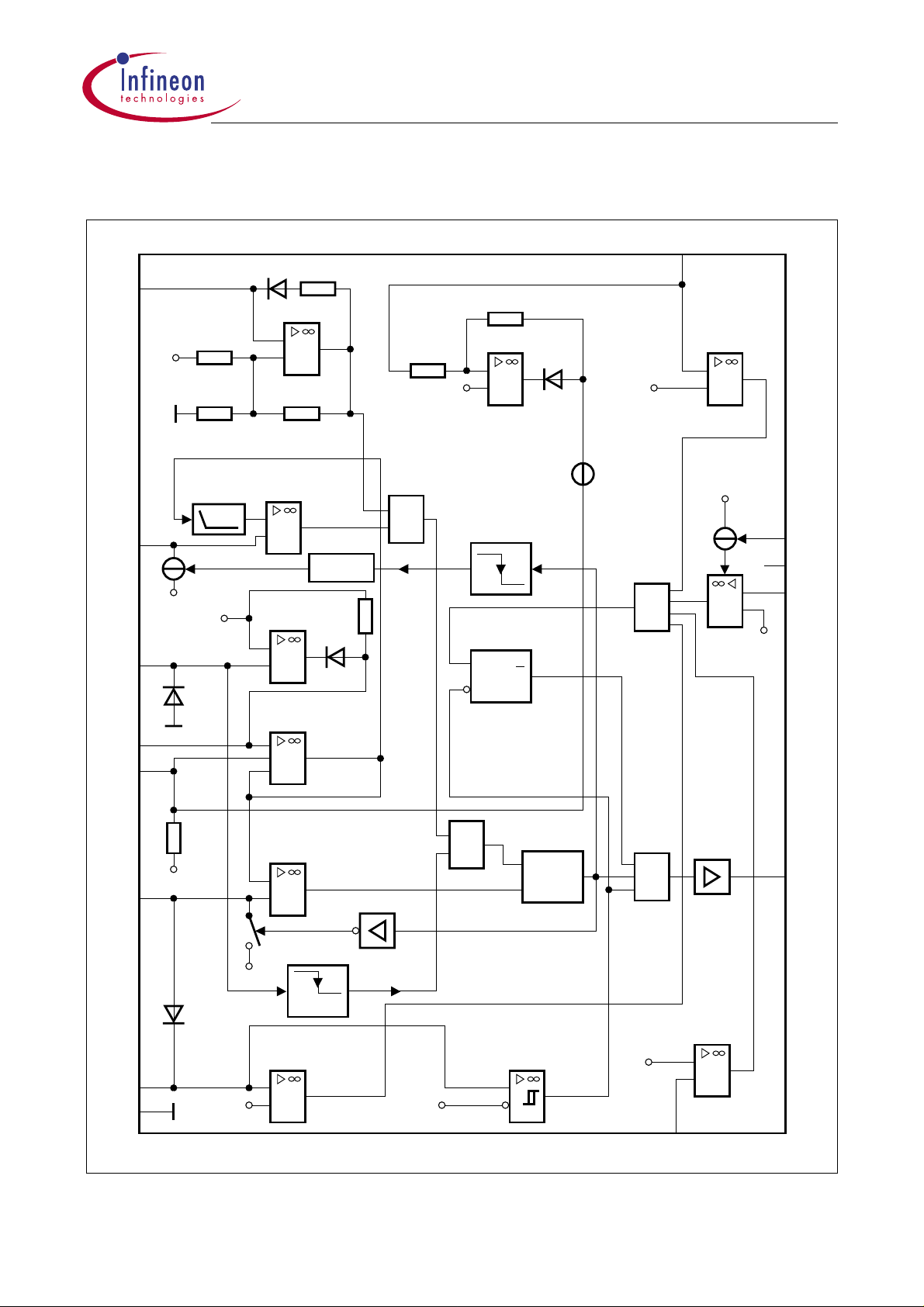
1.5 Block Diagrams
R
SYN
OTC
RZI
SRC
OCI
7
5 V
1
3
4
5
3.5 V
R
7
30 k
Ω
R
8
75 k
Ω
Control Voltage
Limit
2 V
CS1
5 V
D3
D4
Off Time
Comparator
+
-
Error
Amplifier
Buffer for
Control Voltage
KSY
+
R
3
15 k
Ω
RSTC/RSTF
+
-
+
+
-
4
D2
TDA 16846
TDA 16847
PVC
G4
1
11
Primary
Voltage
Check
+
V
CC
FC2
+
-
1.2 V
9
8
6
REF
N.C.
FC2
Fold Back Point Correction
R
x 1/3
6
R
6
PVA
+
D5
1 V
1.5 V
-
G1
+
3.5 V
1
ED2
R
2
Error-
Flipflop
S
Q
R
On Time
Flipflop
S
Q
R
G3
&
Output
Driver
13
OUT
PCS
R
1
20 k
Ω
5 V
2
On Time
Comparator
+
I
1
&
G2
ED1
Zero Crossing
Signal
15/8 V
Supply
Voltage
Comparator
+
-
1 V
10
FC1
FC1
+
AEB02648
V
CC
GND
1.5 V
D1
Startup
Diode
< 25 mV
Overvoltage
Comparator
14
12
1)
The input with the lower voltage becomes operative
16 V
+
-
Figure 2 TDA 16846
Data Sheet 6 2000-01-14
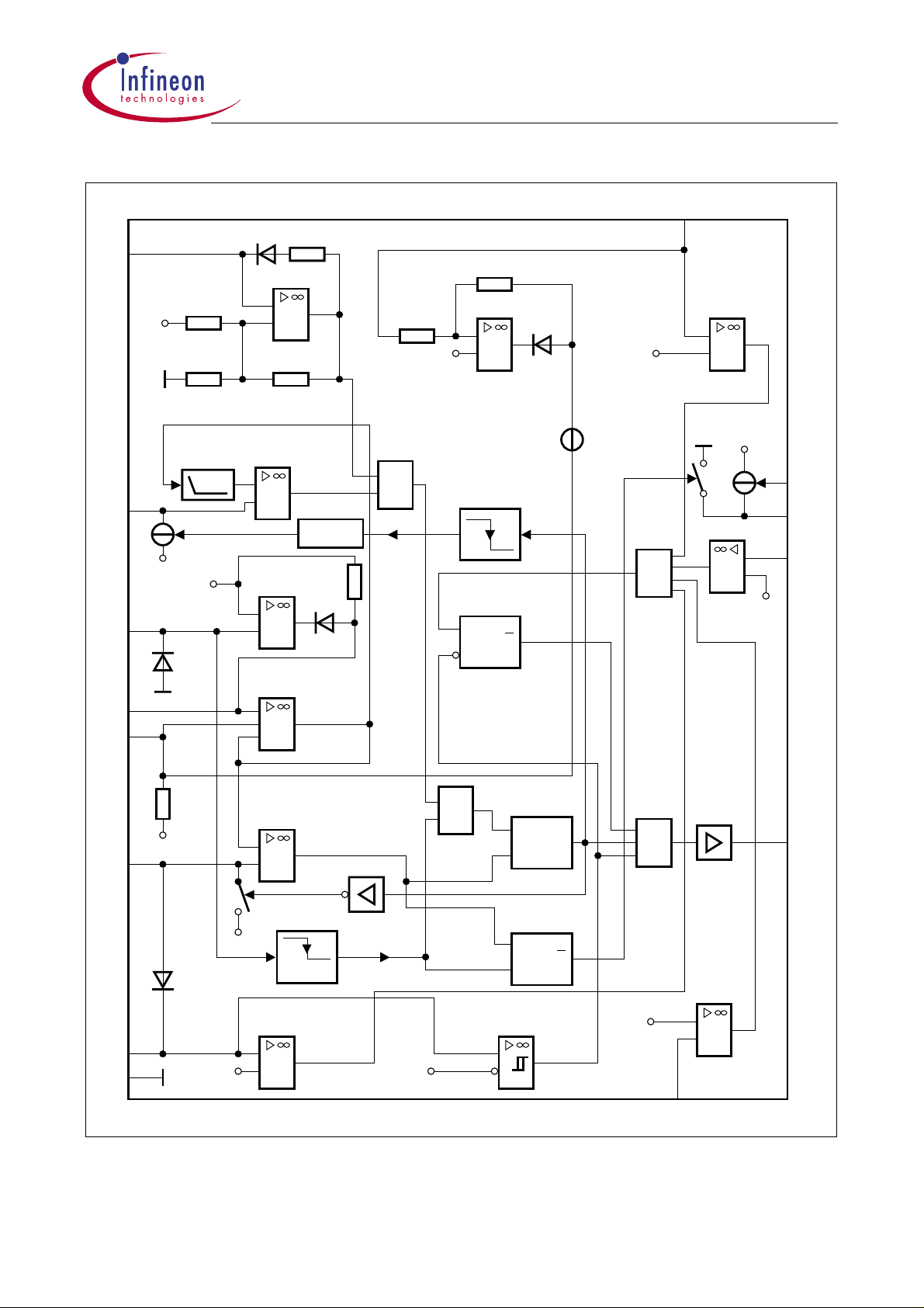
SYN
OTC
RZI
SRC
OCI
7
5 V
1
3.5 V
3
4
5
R
7
30 k
Ω
R
8
75 k
Ω
Control Voltage
Limit
2 V
CS1
5 V
D3
R
D4
4
KSY
+
R
3
15 k
Ω
Off Time
Comparator
+
-
RSTC/RSTF
Error
Amplifier
+
-
Buffer for
Control Voltage
+
+
-
R
D2
1)
TDA 16846
TDA 16847
PVC
G4
1
11
Primary
Voltage
Check
S2
+
V
FC2
CC
+
-
1.2 V
9
8
6
REF
PMO
FC2
Fold Back Point Correction
R
x 1/3
6
R
6
PVA
+
D5
1 V
1.5 V
-
G1
+
3.5 V
1
ED2
2
Error-
Flipflop
S
Q
R
R
PCS
1
20 k
Ω
5 V
2
On Time
Comparator
+
S1
ED1
1.5 V
D1
Startup
Diode
< 25 mV
Overvoltage
Comparator
14
V
CC
GND
12
1)
The input with the lower voltage becomes operative
16 V
+
-
Figure 3 TDA 16847
I
1
15/8 V
&
G2
Zero
Crossing
Signal
Supply Voltage
Comparator
On Time
Flipflop
S
Q
R
Discharge Time
Flipflop
S
Q
R
+
-
1 V
G3
&
10
FC1
Output
Driver
FC1
-
+
13
AEB02737
OUT
Data Sheet 7 2000-01-14
2 Functional Descript io n
Start Up Behaviour (Pin 14)
TDA 16846
TDA 16847
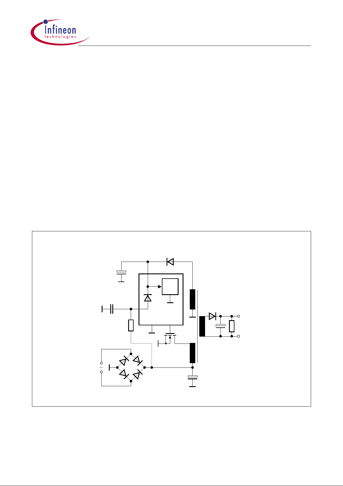
When power is applied to the c hip and the vol tage
V
upper threshold (
) of the Supply Voltage Comparator (SVC), input current I14 will be
ON
V
at Pin 14 (VCC) is less than the
14
less than 100 µA. The chip is not active and driver output (Pin 13) and cont rol output
V
(Pin 4) will be actively held low. When
I
chip starts wor king and
V
) the chip starts again at his initial condition. Figure 4 shows the start-up circuit and
(
OFF
Figure 5 shows the voltage
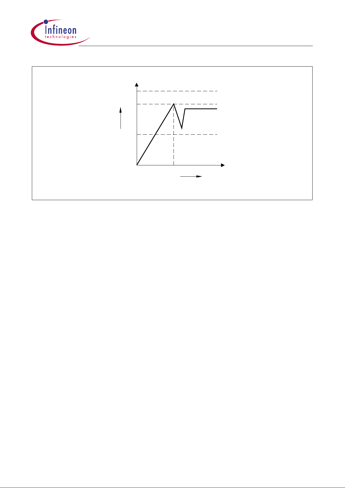
increases. When V14 falls below the lower SVC t hreshold
14
V
during start up. Charging of C14 is done by resistor R2 of
14
exceeds the upper SVC threshold (VON) the
14
the “Primary Current Simu lation” (see later) and t he internal diode D 1, so no additional
C
start up resistor is needed. The capacitor
delivers the supply current until the
14
auxiliary windi ng of the transf ormer supplies the chip with curr ent through the e xternal
diode D14.
It is recommended to sw itch a sm all RF snubber capacitor of e.g. 100 nF para llel to the
electrolytic capacitor at pin 14 as shown in the application circuits in Figures 15, 16, and
17.
D14
V
C
14
C
2
PCS
CC
14
SVC
TR
D1
2
R
2
TDA 16846
V
Out
C
p
AES02649
Figure 4 Startup Circuit
Data Sheet 8 2000-01-14
TDA 16846
TDA 16847
V
max
V
14
V
On
V
Off
Startup Operation
t
AED02650
Figure 5 Startup Voltage Diagram
Primary Current Simulation PCS (Pin 2) / Current Limiting
A voltage proportional to the current of the power transistor is generated at Pin 2 by the
RC-combination R2, C2 (Figure 4). The voltage at Pin 2 is forced to 1.5 V when the
C
power transistor is switched off and during its switch on time
V
the rectified mains. The relation of
:
V
2
L
The vol t ag e
: Primary inductance of the transformer
primary
V
is applied to one input of the On Time Comparator ONTC (see Figure 2).
2
and the current in the power transistor (I
2
1,5 V
L
primaryIprimary
------------------------------- -+=
×
R2C
×
2
is charged by R2 from
2
) is
primary
The other input is the control voltage. If V2 exceeds the control voltage, the driver
switches off (curr ent limiting) . The maxi mum val ue of the control voltage is the i nternal
reference voltage 5 V, so the maximum current in the power transistor (
:
I
Mprimary
) is
3,5 V R2× C2×
I
Mprimary
--------------------------------------=
L
primary
The control voltage can be reduced by either the Error Amplifier EA (current mode
regulation), or by an opto coupler at Pin 5 (re gulation with opto coupler isolation) or by
V
the voltage
Data Sheet 9 2000-01-14
at Pin 11 (Fold Back Point Correction).
11
 Loading...