

Page 1

Data Sheet, Version1.3, July 2003
TDA 16846
TDA 16846-2
TDA 16847
TDA 16847-2
Controller for Switch Mode Power
Supplies Supporting Low Power
Standby and Power Factor
Power Management & Supply
Never stop thinking.
Page 2

TDA 16846/TDA 16846-2
Revision History: Current Version: 2003-07-31
Previous Version Data Sheet TDA 16846: 2000-01-14
Previous Version Data Sheet TDA 16846-2: 2002-07-30
Page
(in previous
Version)
20
21
Page
(in current
Version)
20
21
Subjects (major changes since last revision)
The data sheets for TDA 16846 and TDA 16846-2 have been
combined in this version. Some measuring values are updated:
V
Pin 1 basic value 1
1B1
Pin 2 discharge current
Pin 14 overvoltage
V
14OVmax
Pin 3 delay to switch on
R
I
1min
4ch
Pin 4 charge current
Pull high resistor
and V
I
2DC min
t
slightly decreased.
3d
and discharge current I
changed from 18kOhm to 15 kOhm acc ording
slightly changed.
1B2
changed from 0.5 mA to 0.6 mA.
threshold changed from 17.0 V to 17.1 V.
added.
4DCH
to the data sheet for TDA 16846.
22
23
22
23
Pin 7 charge current
and upper threshold V
7 min
Pin 13 rise and fall time a dapted acco rding to
V
13aclow
slightly decreased (only TDA 16846-2, TDA 16847-2).
C
13
small changed.
7Hmin
= 1nF (prev. 10 nF).
I
TDA 16846-2/TDA 16847-2:
Improvements of TDA 16846-2/TDA16847-2 compared with TDA 16846/TDA16847
Pin 5 OCI Expanded input voltage range down to zero, series resistor between
pin 5 and ground is no longer necessary.
Pin 7 SYN Improved startup to prevent the transformer from saturation also in
fixed frequency and synchronized mode.
Pin 11 PVC Noise-immunity improved by spike blanking.
Pin 13 OUT Reduced output voltage level for off state.
Pin 14 VCC Noise-immunity improved by spike blanking.
Edition 07.03
Published by Infineon Technologies AG
St.-Martin-Strasse 53
D-81541 München
© Infineon Technologies AG 2003
All Rights Reserved.
Attention please!
The information herein is given to describe certain components and shall not be considered as warranted characteristics.
Terms of delivery and rights to technical change reserved.
We hereby disclaim any and all warranties, including but not limited to warranties of non-infringement, regarding circuits, descriptions and
charts stated herein.
Infineon Technologiesis an approved CECC manufacturer.
Information
For further information on technology, delivery terms and conditions and prices please contact your nearest Infineon Technologies Office
in Germany or our Infineon Technologies Representatives worldwide.
Warnings
Due to technical requirements components may contain dangerous substances. For information on the types in question please contact
your nearest Infineon Technologies Office.
Infineon Technologies Components may only be used in life-support devices or systems with the express written approval of Infineon Technologies, if a failure of such components can reasonably be expected to cause the failure of that life-support device or system, or to affect
the safety or effectiveness of that device or system. Life support devices or systems are intended to be implanted in the human body, or to
support and/or maintain and sustain and/or protect human life. If they fail, it is reasonable to assume that the health of the user or other
persons may be endangered.
Page 3
Controller for Switch Mode Power Supplies
Supporting Low Power Standby and Power
Factor Correction
1Overview
1.1 Features
• Line Current Consumption with PFC
• Low Power Consumption
• Stable and Adjustable Standby Frequency
• Very Low Start-up Current
• Soft-Start for Quiet Start-up
• Free usable Fault Comparators
• Synchronization and Fixed Frequen cy Ci rcuits
• Over- and Undervoltage Lockout
• Switch Off at Mains Undervoltage
• Temporary High Power Circuit (only TDA 16847-2)
• Mains Voltage Dependent Fold Back Point Correction
• Continuous Frequency Reduction with Decreasing Load
• Adjustable and Voltage Dependent Ringing Suppression Time
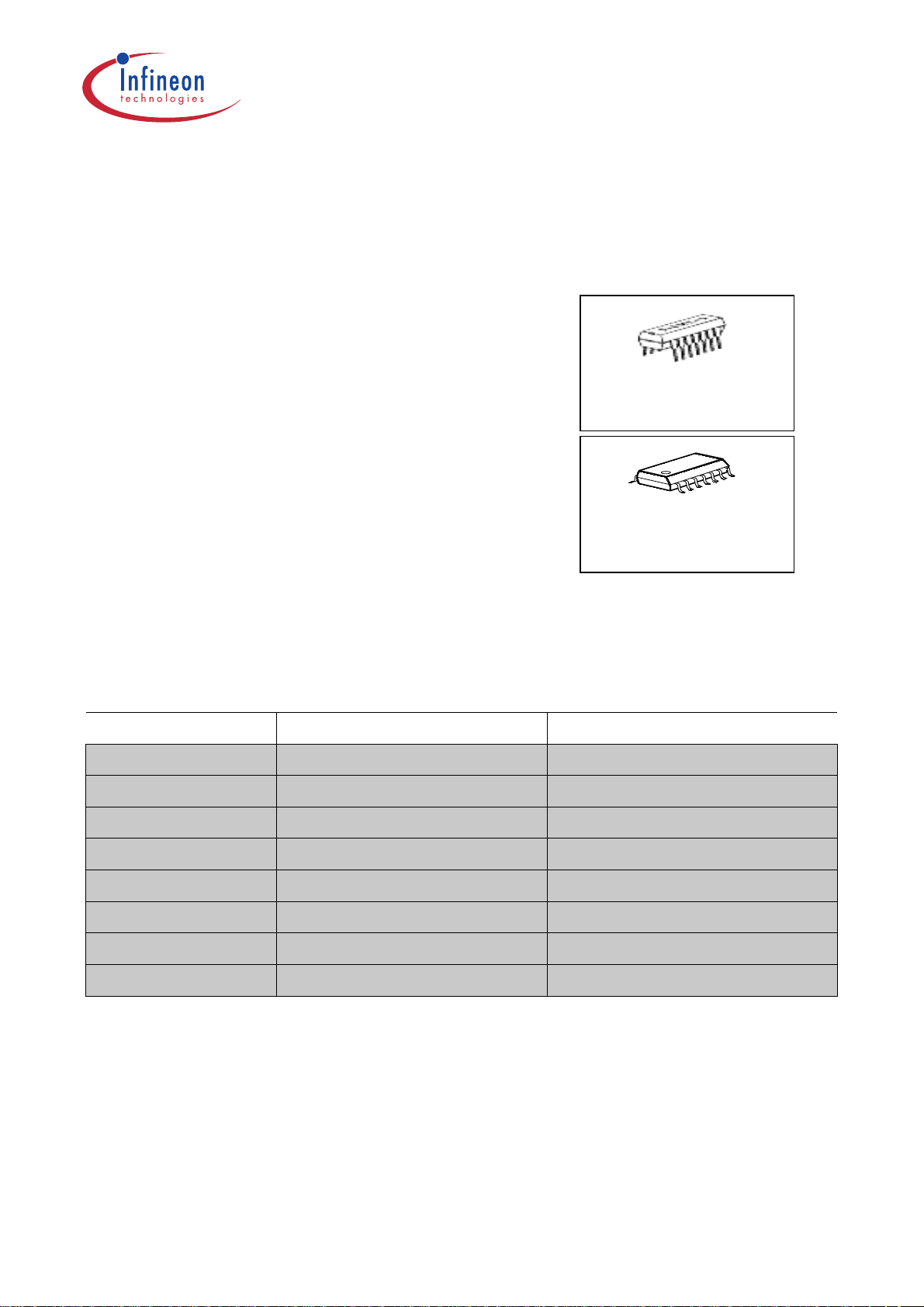
P-DIP-14-3
P-DSO-14-3
TDA 16846
TDA 16846-2
Bipolar IC
Type Ordering Code Package
TDA 16846 Q67000-A9377 P-DIP-14-3
TDA 16847 Q67000-A9378 P-DIP-14-3
TDA 16846G Q67006-A9430 P-DSO-14-3
TDA 16847G Q67006-A9412 P-DSO-14-3
TDA 16846-2 Q67040-S4494 P-DIP-14-3
TDA 16847-2 Q67040-S4496 P-DIP-14-3
TDA 16846-2G Q67040-S4495 P-DSO-14-3
TDA 16847-2G Q67040-S4497 P-DSO-14-3
1.2 Description
The TDA 16846-2 (this name is used in the description for all types) is optimized to
control free running or fixed f requency flyback con verters with or witho ut Power Factor
Correction (Current Pump). To provide low power consumption at light loads, this device
reduces the switching frequency in small steps with load, towards an adjustable
minimum (e. g. 20 kHz in standby mode). Additionally, the startup current is very low. To
avoid switching stress on the power devices, the power transistor is always switched on
at minimum voltage. A special circuit is implemented to avoid jitter. The device has
Data Sheet 3 2003-07-31
Page 4
TDA 16846
TDA 16846-2
several protection function s: VCC over- and undervoltage, ma ins undervoltage, current
limiting and 2 free usable fault comparators. Regulation can be done by using the
internal error amplifier or an opto co upler feedbac k (additional in put). The output driv er
is ideally suited for driving a power MOSFET. Fixed frequency and synchronized
operation are also possible.
The TDA 16846-2 is suited for TV-, VCR- sets, SAT receivers and other sets for
consumer electronics. It also can be used in PC monitors.
The TDA 16847-2 is identical with TDA 16846-2 but has an additional power
measurement output (pin 8) which can be used as a Temporary High Power Circuit.
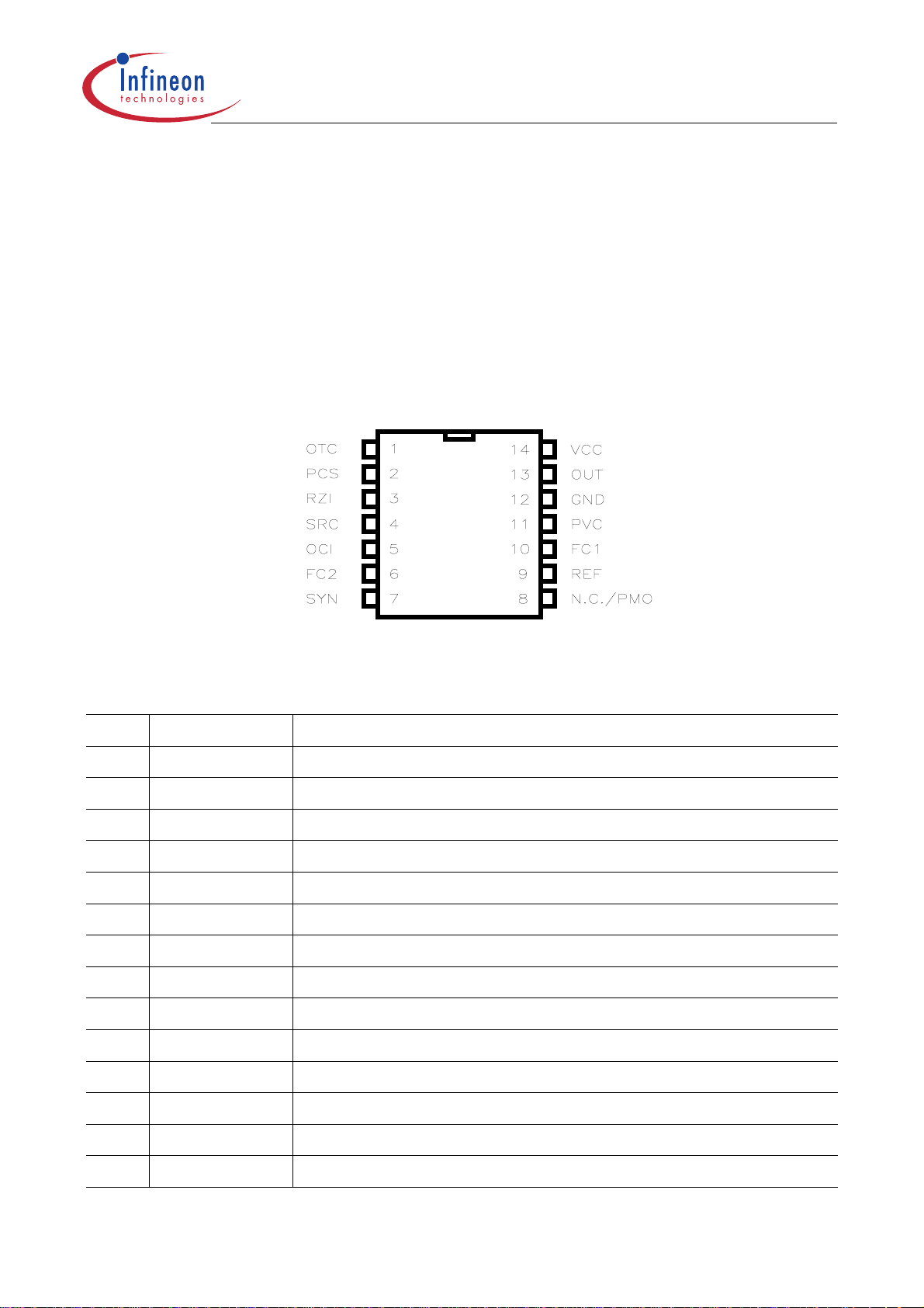
Figure 1 Pin Configuration (top view)
1.3 Pin Definitions and Functions
Pin Symbol Function
1 OTC Off Time Circuit
2 PCS Primary Current Simulation
3 RZI Regulation and Zero Crossing Input
4 SRC Soft-Start and Regulation Capacitor
5 OCI Opto Coupler Input
6 FC2 Fault Comparator 2
7 SYN Synchronization Input
8 N.C./PMO Not Connected (TDA 16846-2) / PMO (TDA 16847-2)
9 REF Reference Voltage and Current
10 FC1 Fault Comparator 1
11 PVC Primary Voltage Check
12 GND Ground
13 OUT Output
14 VCC Supply Voltage
Data Sheet 4 2003-07-31
Page 5

TDA 16846
TDA 16846-2
1.4 Short Description of the Pin Functions
Pin Function
1 A parallel RC-circuit between this pin and ground determines the ringing
suppression time and the standby-frequency.
2 A capacitor between this pin and ground and a resistor between this pin and
the positive terminal of the primary electrolytic capacitor quantifies the max.
possible output power of the SMPS.
3 This is the input of the error amplifier and the zero crossing input. The output
of a voltage divider between the control winding and ground is connected to
this input. If the pulses at pin 3 exceed a 5 V threshold, the control voltage at
pin 4 is lowered.
4 This is the pin for the control voltage. A capacitor has to be connected
between this pin and ground. The value of this capacitor determines the
duration of the softstart and the speed of the control (primary regulation).
5 If an opto coupler for the control is used, its output has to be connected
between this pin and ground. The voltage divider at pin 3 has then to be
changed, so that the pulses at pin 3 are below 5 V.
6 Fault comparator 2: A voltage > 1.2 V at this pin stops the SMPS (v.also pin 9).
7 If fixed frequency mode is wanted, a parallel RC circuit has to be connected
between this pin and ground. The RC-value determines the frequency. If
synchronized mode is wanted, sync pulses have to be fed into this pin.
8 TDA 16846-2: Not connected. TDA 16847-2: This is the power measurement
output of the Temporary High Power Circuit. A capacitor and a RC-circuit has
to be connected between this pin and ground.
9 Output for the reference voltage (5 V). With a resistor between this pin and
ground the fault comparator 2 (pin 6) is enabled.
10 Fault comparator 1: If a voltage > 1 V is applied to this pin, the SMPS stops.
11 This is the input of the primary voltage check. The voltage at the anode of the
primary electrolytic capacitor has to be fed to this pin via a voltage divider. If
the voltage of this pin falls below 1 V, the SMPS is switched off. A second
function of this pin is the primary voltage dependent fold back point correction
(only active in free running mode).
12 Common ground.
13 Output signal. This pin has to be connected via a series resistor to the gate of
the power transistor.
14 Connection for supply voltage and startup capacitor. After startup, the supply
voltage is produced by the control winding of the transformer and rectified by
an external diode.
Data Sheet 5 2003-07-31
Page 6
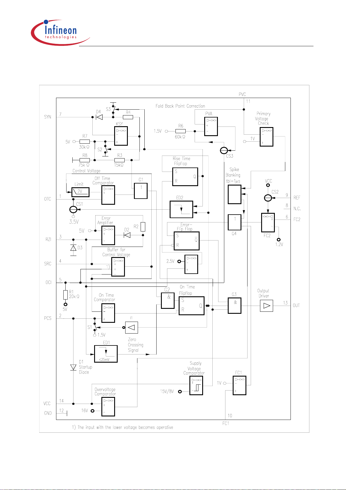
1.5 Block Diagrams
TDA 16846
TDA 16846-2
Figure 2 TDA 16846-2
Data Sheet 6 2003-07-31
Page 7
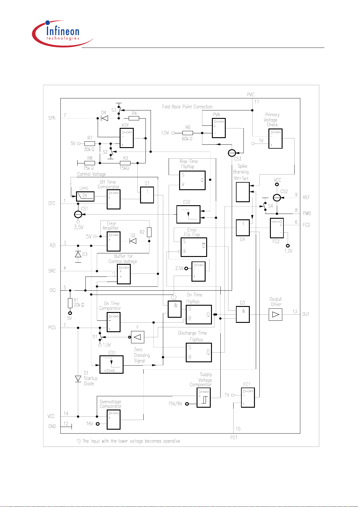
TDA 16846
TDA 16846-2
Figure 3 TDA 16847-2
Data Sheet 7 2003-07-31
Page 8
TDA 16846
TDA 16846-2
2 Functional Description
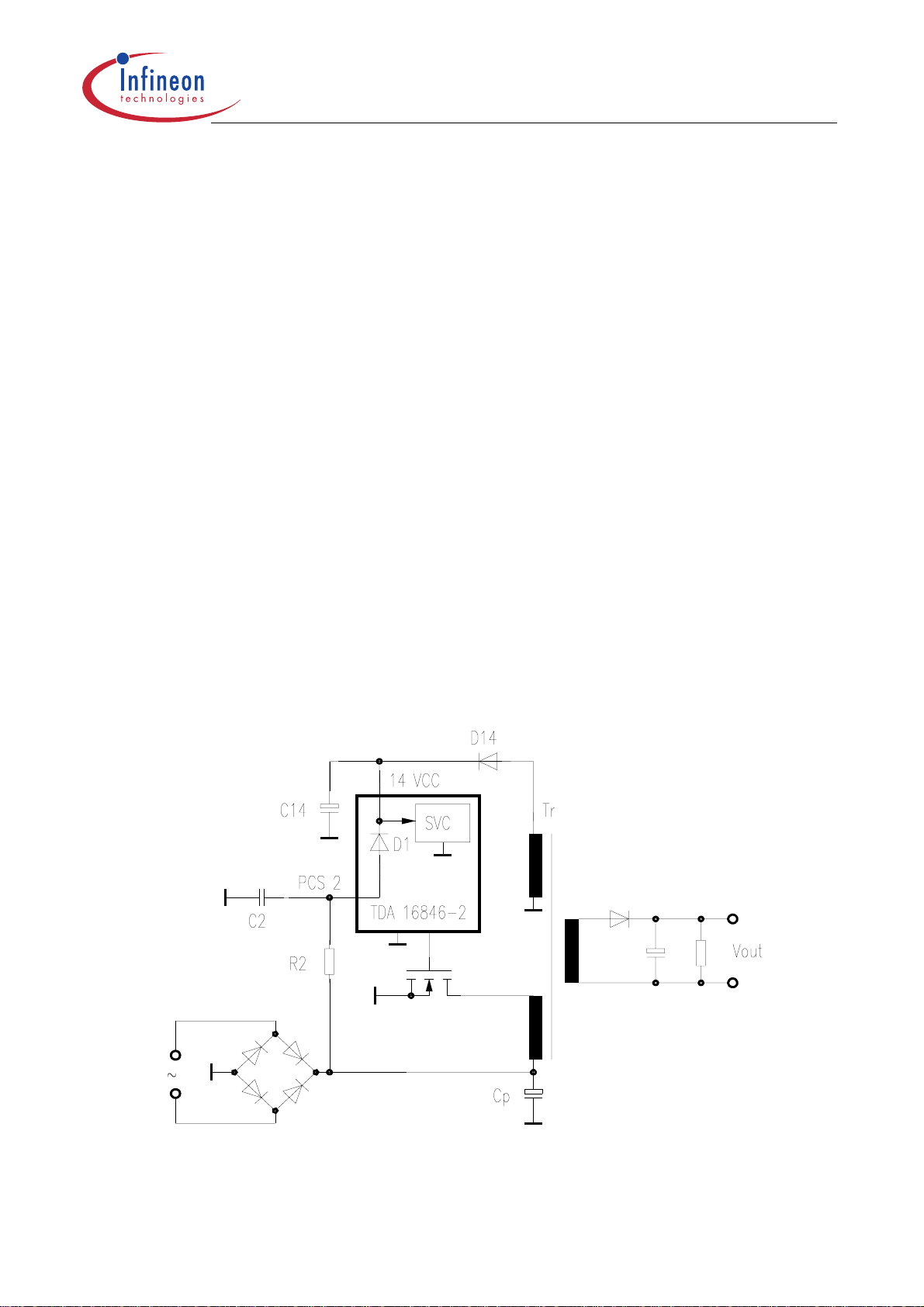
Start Up Behaviour (Pin 14)
V
When power is applied to the chip and the vol tage
V
upper threshold (
I
will be less than 100 µA. The chip is not active (off state) and driver output (Pin 13)
14
) of the Supply Voltage Comparator (SVC), the n the input current
ON
and control output (Pin 4) will be active ly held low. When
threshold (
SVC threshold (
start-up circuit and Figure 5 shows the vo ltage
done by resistor
V
) the chip starts working and I14 increases. When V14 falls below the lower
ON
V
) the chip starts again from its initi al condi tion. Figure 4 shows t he
OFF
V
R
of the “Primary Current Simulation” (see later) and the internal diode
2
D1, so no additional start up resistor is needed. The capacito r
current until the auxiliary winding of the transformer supplies the chip with current
through the external diode D14.
at Pin 14 (VCC) is less than the
14
V
exceeds the upper SVC
14
during start up. Chargi ng of C14 is
14
C
delivers the supply
14
It is recommended to apply a small RF snubber cap acitor of e.g. 100 nF parallel to t he
electrolytic capacitor at pin 14 as shown in the application circuits in Figures 15, 16 , and
17.
To avoid multiple pulses during start up in fixed frequency mode (danger of transformer
saturation), the IC works in freerunni ng mode un til th e pulses at pin 3 (RZ I) exceed the
2.5 V threshold (only TDA 16846-2, TDA 16847-2).
Figure 4 Startup Circuit
Data Sheet 8 2003-07-31
Page 9
TDA 16846
TDA 16846-2
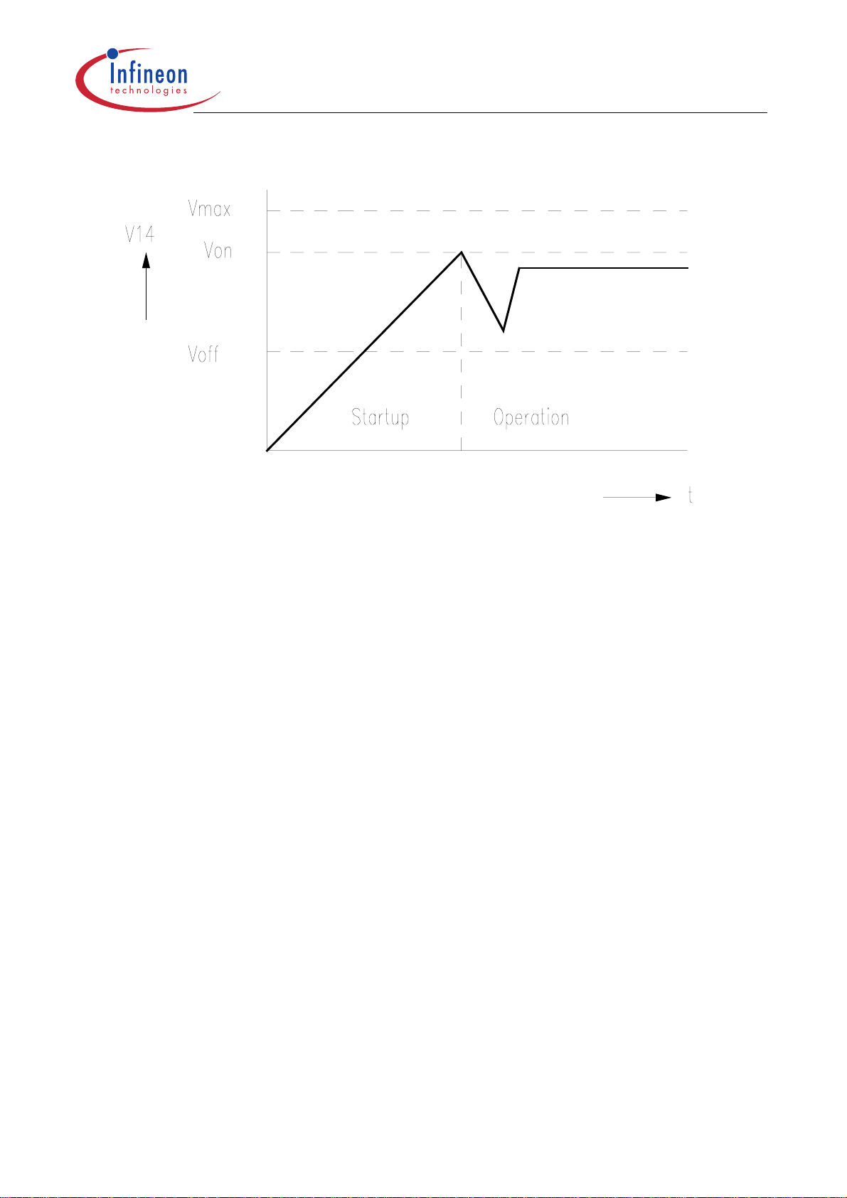
Figure 5 Startup Voltage Diagram
Primary Current Simulation PCS (Pin 2) / Current Limiting
A voltage proportional to the current of the power transistor is generated at Pin 2 by the
RC-combination
power transistor is switched off an d during its switch on time
the rectified mains. The equation of
:
L
: Primary inductance of the transformer
primary
The voltage
The other input is the control voltage. If
R
, C2 (Figure 4). The voltage at Pin 2 is forced to 1.5 V when the
2
C
is charged by R2 from
2
V
and the current in the power transistor (I
2
L
V
V
is applied to one input of the On Time Comparator ONTC (see Figure 2).
2
1,5 V
2
primaryIprimary
--------------------------------+=
V
×
R2C
×
2
exceeds the control voltage, the driver
2
primary
) is
switches off (current limiting ). The maximum valu e of the control vol tage is the internal
reference voltage 5 V, so the maximum current in the power transistor (
:
I
Mprimary
) is
I
Mprimary
--------------------------------------=
L
primary
The control voltage can be reduced by either the Error Amplifier EA (current mode
regulation), or by an opto co upler at Pin 5 (regulation with opto coup ler isolation) or by
3,5 V R2× C2×
the voltage
Data Sheet 9 2003-07-31
V
at Pin 11 (Fold Back Point Correction).
11
Page 10

TDA 16846
TDA 16846-2
Fold Back Point Correction PVC (Pin 11)
V
is derived from a voltag e divider connected to the rectified mains an d reduces the
11
limit of the possible current maximum in the power transistor if the mains voltage
increases. I.e. this limit is indep endent of the mains (only active in free running mode).
The maximum current (
:
Off-Time Circuit OTC (Pin 1)
Figure 6 shows the Off-Time Circuit which determines t he load dependent frequency
curve. When the driver switches off (Figure 7) the capacitor
I
(approx. 0.5 mA, fo r extended ringing suppre ssion time). As soon as the voltage at
1L
pin 3 reaches the level
I
(approx. 1 mA, for normal ringing suppression time). This current flows until the
1H
capacitor’s voltage reaches 3.5 V. The charge time TC1 is
:
I
Mprimary
V
3L
) depending on the voltage V11 at Pin 11 is
I
Mprimary
4V V113⁄–()R
------------------------------------------------------------=
L
primary
C
××
2
2
C
is charged first by current
1
(2.5 V), the charging current is switched to the higher val ue
C
1,5 V×
1
TC1
-------------------------
≈
1mA
For proper operation of the special internal anti- jitter circuit, TC1 (rising time for I1H only)
should have the same value as the re sonanc e time “tR” of the power ci rcui t (Figure 7).
C
After charging
R
resistor
. The voltage V1 at Pin 1 is ap pli ed to the Off-Time Comparator (OFTC ). T he
1
up to 3.5 V the current source is disconnected and C1 is discharged by
1
other input of OFTC is the control vol tage. The va lue of the c ontrol voltag e at the inp ut
of OFTC is limited to a minimum of 2 V (for stable frequency at very light load). The OnTime Flip Flop (ONTF) is set, if the output of OFTC is high
1)
and the voltage V3 at Pin 3
falls below 25 mV (zero crossing signal is high). This ensures switching on of the power
transistor at minimum voltage. If no zero crossing signal is coming into pin 3, the power
transistor is switched on after an additional delay until
OFTCD). As long as
suppress wrong zero cros sings of
after switch-off. The discharge time of
1)
i.e. V1 is less than the limited control voltage.
.
V
is higher than the limit ed control voltage, ON TF is disabled to
1
V
, due to parasitic oscillatio ns from the transformer
3
C
is a function of the control voltage.
1
V
falls below 1.5 V (see Figure 6,
1
Control Voltage Output Power Off-time TD1
1.5 - 2 V Low Constant (TD1
), const. frequency stand by
MAX.
2 - 3.5 V Medium Decreasing
3.5 - 5 V High Free running, switch-on at first minimum
Data Sheet 10 2003-07-31
Page 11

TDA 16846
TDA 16846-2
If the control voltage is below 2 V (at low output power) the “off-time” is maximum and
constant
TD1
max
056, R
× C1×≈
1
During the discharge time tD1, V1 must not fall below the limit
is not guaranteed.
V
, otherwise the function
1L
Figure 6 Off-Time-Circuit
Data Sheet 11 2003-07-31
Page 12

TDA 16846
TDA 16846-2
Figure 7 Pulse Diagram of Off-Time-Circuit
Figure 8 shows the converters switching frequency as a function of the output power.
Figure 8 Load Dependent Frequency Curve
Data Sheet 12 2003-07-31
Page 13

TDA 16846
TDA 16846-2
Error Amplifier EA / Soft-Start (Pin 3, Pin 4)
Figure 9 shows the simplified Error Amplifier circuit. The positive input of the Error
Amplifier (EA) is the reference voltage 5 V. The negative input is the pulsed output
voltage from the auxiliary winding, divided by
dimensioned only for delaying zero crossings and smoothing the first spike after switchoff. Smoothing of the regulation voltage is done with the soft start capacitor
During start up
regulation
C
is charged with a current of approx. 2 µA (Soft Start). For primary
4
C
is charged and discharged with pulsed currents. Figure 10 shows the
4
voltage diagrams of the Error Amplifier circuit.
R
and R32. The capacitor C3 is
31
C
at Pin 4.
4
Figure 9 Error Amplifier
Figure 10 Regulation Pulse Diagram
Data Sheet 13 2003-07-31
Page 14

TDA 16846
TDA 16846-2
Fixed Frequency and Synchronization Circuit SYN (Pin 7)
Figure 11 shows the Fixed Frequency and Synchronization Circuit. The circuit is
disabled when Pin 7 is not connected or connected to pin 9 (Vref, to avoid noise
sensitivity). With
1 mA and disc harged slowly b y
beginning of the charge phase. The switching frequency is (charge time ignored)
:
When the oscillator circuit is working the Fold Back Point Correction is disabled (not
necessary in fixed frequency mode). “Switch on” is only possible when a “zero crossing”
has occurred at Pin 3, otherwi se “switch-on” will be delayed (Figure 12).
R
and C7 at Pin 7 the circuit is working. C7 is charged fast with approx.
7
R
(Figure 11). The power transistor is switched on at
7
08,
--------------
f
≈
R7C
×
7
Figure 11 Synchronization and Fixed Frequency Circuit
Data Sheet 14 2003-07-31
Page 15

TDA 16846
TDA 16846-2
Figure 12 Pulse Diagram for Fixed Frequency Circuit
Synchronization mode is also possible. The s ynchronization frequenc y must be higher
than the oscillator frequency.
Figure 13 Ext. Synchronization Circuit
Data Sheet 15 2003-07-31
Page 16

TDA 16846
TDA 16846-2
3 Protection Functions
The chip has several protection functions:
Current Limiting
See “Primary Current Simulation PCS (Pin 2) / Current L imiting” and “Fold Ba ck Point
Correction PVC (Pin 11)”.
Over- and Undervoltage Lockout OV/SVC (Pin 14)
V
When
Flip Flop ERR is set and the output driver is shut-down. When
SVC threshold, ERR is reset and the driver output (Pin 13) and the soft-start (Pin 4) are
shut down and actively held low.
at Pin 14 exceeds 16.5 V, e. g. due to a fault in the regulation circuit, the Error
14
V
goes below the lower
14
Primary Voltage Check PVC (Pin 11)
When the voltage
V
at Pin 11 go es below 1 V the Error Flip Fl op (ERR) is set. E.g. a
11
voltage divider from the rectified mains at Pin 11 prevents high input currents at a too low
input voltage.
Free Usable Fault Comparator FC1 (Pin 10)
When the voltage at Pin 10 exceeds 1 V, the Error Flip Flop (ERR) is set. This c an be
used e. g. for mains overvoltage shutdown.
Free Usable Fault Comparator FC2 (Pin 6)
When the voltage at Pin 6 exceeds 1.2 V, the Error Flip Flop (ERR) is set. A resis tor
between Pin 9 (REF) and ground is necessary to enable this fault comparator.
Voltage dependent Ringing Suppression Time
During start-up and short-circuit operation, the output voltage of the converter is low and
parasitic zero crossings are applied for a longer time at Pin 3. Therefore the Ringing
Suppression Time TC1 (see “Off-Time Circuit OTC (Pin 1)”) is extended with a factor of
2.2 at a low output voltage. The voltage at pin 1 must not fall below the limit V
1L.
Data Sheet 16 2003-07-31
Page 17

TDA 16846
TDA 16846-2
4 Temporary High Power Circuit FC2, PMO, REF
(Pin 6, 8, 9, TDA 16847-2)
Figure 14 shows the Temporary High Power Circuit:
Figure 14
The Temporary High Power Circuit (THPC) consists of two parts:
Firstly, a power measurement circuit is implemented: The capacitor
charged with a constant current
I
during the discharge time of the flyback transformer
8
and grounded the other t ime. Thus the average of the s awtooth voltage
C
at Pin8 is
8
V
at Pin 8 is
8
proportional to the converter´s output power (at con stant output voltages). The charge
current
I
for C8 is set by the resistor R9 at Pin 9:
8
I
=5V/R
8
9
Data Sheet 17 2003-07-31
Page 18

TDA 16846
TDA 16846-2
Secondly, a High Power Shutdown Comparator (FC2) is implemented: When the voltage
V
at Pin 6 exceeds 1.2 V the Error Flip Flop (ERR) is set. The output voltage of the
6
power measurement circuit (Pin 8) is smoothed by
shutdown” input at Pin 6. The relati on between this voltage
the converter
P is approximately:
R
and applied to the “high power
8/C6
V
and the output powe r of
6
V
6
L
Secondary
V
OUT
So the time constant of
: The transformers secondary inductance
: The converters output voltage
R
R
≈ (P × L
9/C8
× C8≈ (PSD× L
9
Secondary
for a certain high power shutdown level PSD is:
× 5V)/(V
Secondary
2
× C8× R9)
OUT
× 4.2)/V
2
OUT
The converters high p ower shutdown level ca n be adjusted lower (by R9, C8) than the
current limit level (see “current limiting”). Thus because of the delay
R
, the converter
8/C6
can deliver maximum output power (current limit level) for a certain time (e. g. for power
pulses like motor start current) and a power below the high power shutdown level for an
unlimited time. This is of advantage because the thermal dimensioning of the power
devices needs to be d one for the lower p ower level only . Once the v oltage
1.2 V no m ore charging or dischargi ng happens at Pin 8. The voltage
V
exceeds
6
V
remains high
6
due to the bias current out of FC2 and the converter remains switched-off. Reset can be
done either by plugging-off the supply from the mains or by a high value resistor
R
(Figure 14). R6 causes a reset every few seconds. When Pin 9 is not connected or gets
too little current (I9 < I9FC2), the temporary high power circuit is disabled.
6
Data Sheet 18 2003-07-31
Page 19

TDA 16846
TDA 16846-2
5 Electrical Characteristics
5.1 Absolute Maximum Ratings
All voltages listed are referenced to ground (0 V, VSS) except where noted.
Parameter Symbol Limit Values Unit Remarks
min. max.
Supply Voltage at Pin 14
V
CC
–0.3 17 V –
Voltage at Pin 1, 4, 5, 6, 7, 9, 10 – – 0.3 6 V –
Voltage at Pin 2, 8, 11 – – 0.3 17 V –
Startup current into Pin 2
Voltage at Pin 3
Current into Pin 3
Current into Pin 9
Current into Pin 13
I
2
RZI
I
REF
I
OUT
1mA
6V
–10
mA
V
–1 – mA –
– 100
100 mA
mA
V
V
< – 0.3 V
3
> V
13
13
CC
< 0 V
ESD Protection – – 2 kV MIL STD 883C
method 3015.6,
100 pF, 1500 Ω
Storage Temperature
Operating Junction Temperature
Thermal Resistance
T
T
R
stg
J
thJA
– 65 125 °C–
– 25 125 °C–
– 110 K/W P-DIP-14-3
Junction-Ambient
Soldering Temperature – – 260 °C–
Soldering Time – – 10 s –
Note: Stress beyond the above listed values may cause permanent damage to the
device. Exposure to absolute maximum rated conditions for extended periods may
affect device reliability.
Data Sheet 19 2003-07-31
Page 20

TDA 16846
TDA 16846-2
5.2 Characteristics
Unless othe rwise stated, – 25 °C<Tj< 125 °C, VCC=12V
Parameter Symbol Limit Values Unit Test Condition
min. typ. max.
Supply Voltage and Startup Circuit VCC (Pin 14)
Overvoltage threshold
Turn-ON threshold
Turn-OFF threshold
Delta-OV-
V
14 ON
Supply current, OFF
Supply current, ON
V
14
OV
V
14
ON
V
14
OFF
–0.5––V–
I
14OFF
I
14ON
15.7 16.5 17.1 V
14.5 15 15.5 V –
7.5 8 8.5 V –
–40100µA VCC = V
– 5 8 mA Output low
Primary Current Simulation PCS (Pin 2) / Current Limiting
Basic value V
Peak value
Discharge current
V
I
2DC
2
2
1.45 1.5 1.55 V I2 = 100 µA
4.85 5 5.15 V V11 = 1.2 V
0.6 1.0 2.5 mA V2 = 3 V
Bias current Pin 2 – – 1.0 – 0.3 – µA
Fold Back Point Correction PVC (Pin 11)
mV
V
2
= 2 V
14
ON
-100
Peak value V
5
Bias current Pin 11 – – 1.0 – 0.3 – µA
3.8 4.1 4.3 V V11 = 4.5 V
V
= 1.5 V
11
Off-Time Circuit OTC (Pin 1)
Charge current I
Charge current I
Peak value V
Basic value 1
Basic value 2
V
Lower limit V
1
V
V
1H
1L
1P
1B1
1B2
1L
Bias current Pin 1 – – 1.1 – 0.4 – µA
Data Sheet 20 2003-07-31
0.9 1.1 1.4 mA V3 > V
0.35 0.5 0.65 mA V3 < V
3.38 3.5 3.62 V –
1.9 2 2.1 V –
1.44 1.5 1.58 V –
80 140 mV
V
= 2.2 V
1
3L
3L
Page 21

TDA 16846
TDA 16846-2
5.2 Characteristics (cont’d)
Unless otherwise stated, – 25 °C<Tj<125°C, VCC=12V
Parameter Symbol Limit Values Unit Test Condition
min. typ. max.
Zero Crossing Input RZI (Pin 3)
Zero crossing threshold
15 25 35 mV –
(Pin 3)
Delay to switch-on
t
3d
250 350 460 ns –
Bias current Pin 3 – –2 – 1.2 – µA
Error Amplifier Input RZI (Pin 3)
Input threshold (Pin 3) V
Low voltage threshold (Pin 3)
V
EATH
3L
4.85 5 5.15 V –
2.4 2.5 2.6 V –
Bias current Pin 3 – – – 0.9 – µA
Softstart and Regulation Voltage SRC (Pin 4)
Soft-start charge current
I
4CHS
– 2.5 – 1.8 – 1.2 µA V4 = 2 V
(Pin 4)
Charge current Pin 4
Discharge current Pin 4
I
4CH
I
4DCH
-0.9 -0.7 -0.5 mA
0.9 1.4 1.9 mA
V
V
3
3
= 0 V
= 3 V
Opto Coupler Input OCI (Pin 5)
Input voltage range (TDA
V
5
0.3 – 6 V –
16846, TDA 16847)
Input voltage range (TDA
V
5
0–6V–
16846-2, TDA 16847-2)
Pull high resistor to
Data Sheet 21 2003-07-31
V
REF
R
1
15 20 28 kΩ –
Page 22

TDA 16846
TDA 16846-2
5.2 Characteristics (cont’d)
Unless othe rwise stated, – 25 °C<Tj< 125 °C, VCC=12V
Parameter Symbol Limit Values Unit Test Condition
min. typ. max.
Fixed Frequency and Synchronization Circuit SYN (Pin 7)
Charge current
Upper threshold
Lower threshold
Input voltage range
I
V
V
V
7
7H
7L1
7L2
-0.9 -1.3 -1.6 mA –
3.4 3.6 3.7 V –
1.53 1.6 1.67 V –
0.4 6 V –
Bias current Pin 7 – – 2.4 – 1.8 – 1.1 µA
Primary Voltage Check PVC (Pin 11)
Threshold V
11
0.95 1 1.06 V –
Reference Voltage REF (Pin 9)
Voltage at Pin 9 V
Current to enable FC2
9
I
9FC2
4.8 5 5.15 V I9=–100µA
–18 –7 µA
V
7
=4 V
Data Sheet 22 2003-07-31
Page 23

TDA 16846
TDA 16846-2
5.2 Characteristics (cont’d)
Unless otherwise stated, – 25 °C<Tj<125°C, VCC=12V
Parameter Symbol Limit Values Unit Test Condition
min. typ. max.
Fault Comparator FC2 (Pin 6)
HPC Threshold
Bias Current Pin 6 – – 1.0 – 0.3 0.1 µA
V
6
1.12 1.2 1.28 V –
V
=0.8V
6
Fault Comparator FC1 (Pin 10)
Threshold V
10
Bias current Pin 10 – 0.35 0.65 0.95 µA
0.95 1 1.06 V –
V
10
=0.8V
Power Measurement Output PMO (Pin 8, only TDA 16847, TDA 16847-2)
Charge current Pin 8 I
8
–110 –100 –90 µA I9=–100µA
Output Driver OUT (Pin 13)
Output voltage low state V
Output voltage high state
Output voltage during low
V
(TDA 16846, TDA 16847)
14
V
V
13
13
13
low
high
aclow
1.1 1.8 2.4 V I13 = 100 mA
9.2 10 11 V I13 = – 100 mA
0.8 1.8 2.5 V I13 = 10 mA,
V
= 7 V
14
Output voltage during low
V
(TDA 16846-2, TDA
14
V
13
aclow
0.5 1 1.5 V I13 = 10 mA,
V
= 7 V
14
16847-2)
C
Rise time – 30 50 100 ns
Fall time – 102050ns
= 1 nF,
13
V
=2…8V
13
C
= 1 nF,
13
V
=2…8V
13
Note: The listed characteristics are en sured over the op erating range of t he integrated
circuit. Typical c haracte ristics spec ify me an val ues e xpected over the pro duction
spread. If not otherwise spe cified, typi cal characte ristics appl y at
T
= 25 °C and
A
the given supply voltage.
Data Sheet 23 2003-07-31
Page 24

TDA 16846
TDA 16846-2
Figure 15 Circuit Diagram for Application with PFC
Data Sheet 24 2003-07-31
Page 25

TDA 16846
TDA 16846-2
Figure 16 Circuit Diagram for Standard Application
Data Sheet 25 2003-07-31
Page 26

TDA 16846
TDA 16846-2
Figure 17 Circuit Diagram for Application with Temporary High Power Circuit
Data Sheet 26 2003-07-31
Page 27

Package Outlines
P-DIP-14-3
(Plastic Dual In-line Package)
TDA 16846
TDA 16846-2
Sorts of Packing
Package outlines for tubes, trays etc. are contained in our
Data Book "Package Information".
GPD05584
Dimensions in mm
Data Sheet 27 2003-07-31
Page 28

P-DSO-14-3
(Plastic Dual In-line Package)
TDA 16846
TDA 16846-2
Sorts of Packing
Package outlines for tubes, trays etc. are contained in our
Data Book "Package Information".
Dimensions in mm
Data Sheet 28 2003-07-31
Page 29

This datasheet has been download from:
www.datasheetcatalog.com
Datasheets for electronics components.
 Loading...