

Page 1

User Manual Please read the Important Notice and Warnings at the end of this document V1.0
www.infineon.com
TriBoard TC3X3 TH V1.0 and TriBoard TC3X3 V1.0 2020-05
TriBoard TC3X3
TriBoard Manual TC3X3
Hardware: TriBoard TC3X3 TH V1.0 and TriBoard TC3X3 V1.0
About this document
Scope and purpose
The User Manual provide information about using, configuration and connecting the TriBoard with Infineon
AURIX™ TC3X3 TQFP device (0.4mm pitch). The manual provide information for different hardware types. There
exist different hardware with Through Hole socket (TriBoard TC3X3 TH) and soldered devices (TriBoard TC3X3).
The schematic is identically for the all boards if not other mentioned in chapter schematic. The placing on the
boards is the same, all components are on the same location.
Intended audience
Design, verfication, test and software engineers will use this document to get an understanding of the
functionality and connections of the TriBoard.
Page 2

TriBoard Manual TC3X3
Hardware: TriBoard TC3X3 TH V1.0 and TriBoard TC3X3 V1.0
Table of Contents
Table of Contents
About this document. . . . . . . . . . . . . . . . . . . . . . . . . . . . . . . . . . . . . . . . . . . . . . . . . . . . . . . . . Preface-1
Table of Contents . . . . . . . . . . . . . . . . . . . . . . . . . . . . . . . . . . . . . . . . . . . . . . . . . . . . . . . . . . . . . . TOC-2
1 Introduction . . . . . . . . . . . . . . . . . . . . . . . . . . . . . . . . . . . . . . . . . . . . . . . . . . . . . . . . . . . . . . . . . . . . . 1-1
2 Features . . . . . . . . . . . . . . . . . . . . . . . . . . . . . . . . . . . . . . . . . . . . . . . . . . . . . . . . . . . . . . . . . . . . . . . . . 2-1
2.1 Summary of Features . . . . . . . . . . . . . . . . . . . . . . . . . . . . . . . . . . . . . . . . . . . . . . . . . . . . . . . . . . . . . . . . . . . . . . . 2-1
2.2 Block Diagram . . . . . . . . . . . . . . . . . . . . . . . . . . . . . . . . . . . . . . . . . . . . . . . . . . . . . . . . . . . . . . . . . . . . . . . . . . . . . 2-2
2.3 Placement . . . . . . . . . . . . . . . . . . . . . . . . . . . . . . . . . . . . . . . . . . . . . . . . . . . . . . . . . . . . . . . . . . . . . . . . . . . . . . . . . 2-3
3 TriBoard Information . . . . . . . . . . . . . . . . . . . . . . . . . . . . . . . . . . . . . . . . . . . . . . . . . . . . . . . . . . . . . . 3-1
3.1 Soldered board . . . . . . . . . . . . . . . . . . . . . . . . . . . . . . . . . . . . . . . . . . . . . . . . . . . . . . . . . . . . . . . . . . . . . . . . . . . . 3-1
3.2 Socketed board . . . . . . . . . . . . . . . . . . . . . . . . . . . . . . . . . . . . . . . . . . . . . . . . . . . . . . . . . . . . . . . . . . . . . . . . . . . . 3-1
3.2.1 Usable devices . . . . . . . . . . . . . . . . . . . . . . . . . . . . . . . . . . . . . . . . . . . . . . . . . . . . . . . . . . . . . . . . . . . . . . . . . . . 3-1
3.2.2 Restricted usable devices . . . . . . . . . . . . . . . . . . . . . . . . . . . . . . . . . . . . . . . . . . . . . . . . . . . . . . . . . . . . . . . . . . 3-1
3.3 Power Supply . . . . . . . . . . . . . . . . . . . . . . . . . . . . . . . . . . . . . . . . . . . . . . . . . . . . . . . . . . . . . . . . . . . . . . . . . . . . . . 3-1
3.3.1 Failsafe handling . . . . . . . . . . . . . . . . . . . . . . . . . . . . . . . . . . . . . . . . . . . . . . . . . . . . . . . . . . . . . . . . . . . . . . . . . 3-2
3.4 LEDs . . . . . . . . . . . . . . . . . . . . . . . . . . . . . . . . . . . . . . . . . . . . . . . . . . . . . . . . . . . . . . . . . . . . . . . . . . . . . . . . . . . . . . 3-2
3.5 Clock . . . . . . . . . . . . . . . . . . . . . . . . . . . . . . . . . . . . . . . . . . . . . . . . . . . . . . . . . . . . . . . . . . . . . . . . . . . . . . . . . . . . . . 3-3
3.6 USB Connector . . . . . . . . . . . . . . . . . . . . . . . . . . . . . . . . . . . . . . . . . . . . . . . . . . . . . . . . . . . . . . . . . . . . . . . . . . . . . 3-3
3.6.1 Serial Connection to PC . . . . . . . . . . . . . . . . . . . . . . . . . . . . . . . . . . . . . . . . . . . . . . . . . . . . . . . . . . . . . . . . . . . 3-3
3.6.2 miniWiggler JDS . . . . . . . . . . . . . . . . . . . . . . . . . . . . . . . . . . . . . . . . . . . . . . . . . . . . . . . . . . . . . . . . . . . . . . . . . . 3-4
3.7 FlexRay™ (E-RAY) . . . . . . . . . . . . . . . . . . . . . . . . . . . . . . . . . . . . . . . . . . . . . . . . . . . . . . . . . . . . . . . . . . . . . . . . . . . 3-4
3.8 Serial EEPROM . . . . . . . . . . . . . . . . . . . . . . . . . . . . . . . . . . . . . . . . . . . . . . . . . . . . . . . . . . . . . . . . . . . . . . . . . . . . . 3-4
3.9 MultiCAN . . . . . . . . . . . . . . . . . . . . . . . . . . . . . . . . . . . . . . . . . . . . . . . . . . . . . . . . . . . . . . . . . . . . . . . . . . . . . . . . . . 3-4
3.10 LIN . . . . . . . . . . . . . . . . . . . . . . . . . . . . . . . . . . . . . . . . . . . . . . . . . . . . . . . . . . . . . . . . . . . . . . . . . . . . . . . . . . . . . . . . 3-4
3.11 ADC . . . . . . . . . . . . . . . . . . . . . . . . . . . . . . . . . . . . . . . . . . . . . . . . . . . . . . . . . . . . . . . . . . . . . . . . . . . . . . . . . . . . . . . 3-5
3.12 Other peripherals . . . . . . . . . . . . . . . . . . . . . . . . . . . . . . . . . . . . . . . . . . . . . . . . . . . . . . . . . . . . . . . . . . . . . . . . . . 3-7
3.13 Toggle LED’s . . . . . . . . . . . . . . . . . . . . . . . . . . . . . . . . . . . . . . . . . . . . . . . . . . . . . . . . . . . . . . . . . . . . . . . . . . . . . . . 3-7
3.14 Buttons . . . . . . . . . . . . . . . . . . . . . . . . . . . . . . . . . . . . . . . . . . . . . . . . . . . . . . . . . . . . . . . . . . . . . . . . . . . . . . . . . . . 3-7
3.15 Debug System . . . . . . . . . . . . . . . . . . . . . . . . . . . . . . . . . . . . . . . . . . . . . . . . . . . . . . . . . . . . . . . . . . . . . . . . . . . . . 3-7
3.15.1 OCDS1 . . . . . . . . . . . . . . . . . . . . . . . . . . . . . . . . . . . . . . . . . . . . . . . . . . . . . . . . . . . . . . . . . . . . . . . . . . . . . . . . . . . 3-7
3.15.2 DAP . . . . . . . . . . . . . . . . . . . . . . . . . . . . . . . . . . . . . . . . . . . . . . . . . . . . . . . . . . . . . . . . . . . . . . . . . . . . . . . . . . . . . 3-7
3.15.3 DAP_SCR . . . . . . . . . . . . . . . . . . . . . . . . . . . . . . . . . . . . . . . . . . . . . . . . . . . . . . . . . . . . . . . . . . . . . . . . . . . . . . . . 3-7
3.15.4 High speed with DAP . . . . . . . . . . . . . . . . . . . . . . . . . . . . . . . . . . . . . . . . . . . . . . . . . . . . . . . . . . . . . . . . . . . . . . 3-8
3.15.5 ETK connector (optional) . . . . . . . . . . . . . . . . . . . . . . . . . . . . . . . . . . . . . . . . . . . . . . . . . . . . . . . . . . . . . . . . . . 3-8
3.15.6 EmW Power (optional) . . . . . . . . . . . . . . . . . . . . . . . . . . . . . . . . . . . . . . . . . . . . . . . . . . . . . . . . . . . . . . . . . . . . 3-8
4 TriBoard Configuration . . . . . . . . . . . . . . . . . . . . . . . . . . . . . . . . . . . . . . . . . . . . . . . . . . . . . . . . . . . . 4-1
4.1 HW Boot Configuration . . . . . . . . . . . . . . . . . . . . . . . . . . . . . . . . . . . . . . . . . . . . . . . . . . . . . . . . . . . . . . . . . . . . . 4-1
4.1.1 Default Pad State . . . . . . . . . . . . . . . . . . . . . . . . . . . . . . . . . . . . . . . . . . . . . . . . . . . . . . . . . . . . . . . . . . . . . . . . . 4-1
4.1.2 Bootmode . . . . . . . . . . . . . . . . . . . . . . . . . . . . . . . . . . . . . . . . . . . . . . . . . . . . . . . . . . . . . . . . . . . . . . . . . . . . . . . 4-1
4.2 Assembly Options . . . . . . . . . . . . . . . . . . . . . . . . . . . . . . . . . . . . . . . . . . . . . . . . . . . . . . . . . . . . . . . . . . . . . . . . . . 4-2
4.2.1 General optional resistors . . . . . . . . . . . . . . . . . . . . . . . . . . . . . . . . . . . . . . . . . . . . . . . . . . . . . . . . . . . . . . . . . 4-2
4.2.2 Resistors for peripherals . . . . . . . . . . . . . . . . . . . . . . . . . . . . . . . . . . . . . . . . . . . . . . . . . . . . . . . . . . . . . . . . . . 4-4
5 Signal (on board used) Description . . . . . . . . . . . . . . . . . . . . . . . . . . . . . . . . . . . . . . . . . . . . . . . . . . 5-1
5.1 Power Signals . . . . . . . . . . . . . . . . . . . . . . . . . . . . . . . . . . . . . . . . . . . . . . . . . . . . . . . . . . . . . . . . . . . . . . . . . . . . . . 5-1
5.2 Reset Signals . . . . . . . . . . . . . . . . . . . . . . . . . . . . . . . . . . . . . . . . . . . . . . . . . . . . . . . . . . . . . . . . . . . . . . . . . . . . . . 5-1
5.3 Config Signals . . . . . . . . . . . . . . . . . . . . . . . . . . . . . . . . . . . . . . . . . . . . . . . . . . . . . . . . . . . . . . . . . . . . . . . . . . . . . . 5-2
5.4 Clock Signals . . . . . . . . . . . . . . . . . . . . . . . . . . . . . . . . . . . . . . . . . . . . . . . . . . . . . . . . . . . . . . . . . . . . . . . . . . . . . . 5-2
User Manual TOC-2 V1.0
TriBoard TC3X3 TH V1.0 and TriBoard TC3X3 V1.0 2020-05
Page 3

TriBoard Manual TC3X3
Hardware: TriBoard TC3X3 TH V1.0 and TriBoard TC3X3 V1.0
Table of Contents
5.5 Debug Signals . . . . . . . . . . . . . . . . . . . . . . . . . . . . . . . . . . . . . . . . . . . . . . . . . . . . . . . . . . . . . . . . . . . . . . . . . . . . . . 5-2
5.6 Peripheral Signals . . . . . . . . . . . . . . . . . . . . . . . . . . . . . . . . . . . . . . . . . . . . . . . . . . . . . . . . . . . . . . . . . . . . . . . . . . 5-2
6 Connector Pin Assignment . . . . . . . . . . . . . . . . . . . . . . . . . . . . . . . . . . . . . . . . . . . . . . . . . . . . . . . . . 6-1
6.1 On Board only used signals . . . . . . . . . . . . . . . . . . . . . . . . . . . . . . . . . . . . . . . . . . . . . . . . . . . . . . . . . . . . . . . . . . 6-1
6.2 TC3X3 Connector / Top View . . . . . . . . . . . . . . . . . . . . . . . . . . . . . . . . . . . . . . . . . . . . . . . . . . . . . . . . . . . . . . . . . 6-2
6.3 Power connector pinout . . . . . . . . . . . . . . . . . . . . . . . . . . . . . . . . . . . . . . . . . . . . . . . . . . . . . . . . . . . . . . . . . . . . 6-4
6.4 USB connector pinout . . . . . . . . . . . . . . . . . . . . . . . . . . . . . . . . . . . . . . . . . . . . . . . . . . . . . . . . . . . . . . . . . . . . . . 6-4
6.5 FlexRay™ (ERAY) connector pinout . . . . . . . . . . . . . . . . . . . . . . . . . . . . . . . . . . . . . . . . . . . . . . . . . . . . . . . . . . . 6-4
6.6 CAN connector pinout . . . . . . . . . . . . . . . . . . . . . . . . . . . . . . . . . . . . . . . . . . . . . . . . . . . . . . . . . . . . . . . . . . . . . . 6-4
6.7 LIN connector pinout . . . . . . . . . . . . . . . . . . . . . . . . . . . . . . . . . . . . . . . . . . . . . . . . . . . . . . . . . . . . . . . . . . . . . . . 6-5
6.8 OCDS1 connector pinout . . . . . . . . . . . . . . . . . . . . . . . . . . . . . . . . . . . . . . . . . . . . . . . . . . . . . . . . . . . . . . . . . . . . 6-5
6.9 DAP connector pinout . . . . . . . . . . . . . . . . . . . . . . . . . . . . . . . . . . . . . . . . . . . . . . . . . . . . . . . . . . . . . . . . . . . . . . 6-5
6.10 ETK connector pinout . . . . . . . . . . . . . . . . . . . . . . . . . . . . . . . . . . . . . . . . . . . . . . . . . . . . . . . . . . . . . . . . . . . . . . . 6-6
6.11 Ethernet miniWiggler power connector pinout . . . . . . . . . . . . . . . . . . . . . . . . . . . . . . . . . . . . . . . . . . . . . . . . 6-6
7 Schematic and Layout . . . . . . . . . . . . . . . . . . . . . . . . . . . . . . . . . . . . . . . . . . . . . . . . . . . . . . . . . . . . . 7-1
7.1 Known problems . . . . . . . . . . . . . . . . . . . . . . . . . . . . . . . . . . . . . . . . . . . . . . . . . . . . . . . . . . . . . . . . . . . . . . . . . . . 7-1
7.1.1 Known problems on TriBoard TC3X3 TH V1.0 . . . . . . . . . . . . . . . . . . . . . . . . . . . . . . . . . . . . . . . . . . . . . . . . 7-1
7.1.2 Known problems on TriBoard TC3X3 V1.0 . . . . . . . . . . . . . . . . . . . . . . . . . . . . . . . . . . . . . . . . . . . . . . . . . . . 7-1
7.2 Schematic . . . . . . . . . . . . . . . . . . . . . . . . . . . . . . . . . . . . . . . . . . . . . . . . . . . . . . . . . . . . . . . . . . . . . . . . . . . . . . . . . 7-1
7.3 Layout . . . . . . . . . . . . . . . . . . . . . . . . . . . . . . . . . . . . . . . . . . . . . . . . . . . . . . . . . . . . . . . . . . . . . . . . . . . . . . . . . . . . 7-9
7.4 Layout with Dimensioning . . . . . . . . . . . . . . . . . . . . . . . . . . . . . . . . . . . . . . . . . . . . . . . . . . . . . . . . . . . . . . . . . 7-11
User Manual TOC-3 V1.0
TriBoard TC3X3 TH V1.0 and TriBoard TC3X3 V1.0 2020-05
Page 4

TriBoard Manual TC3X3
Hardware: TriBoard TC3X3 TH V1.0 and TriBoard TC3X3 V1.0
Introduction
1Introduction
We congratulate you on your purchase of the TriCore™ Evaluation Board. This kit is a versatile tool, providing
quick access to the capabilities of TriCore™’s powerful architecture.
Applications can be developed easily. The Evaluation Board is equipped with a variety of memories and
peripherals for connection to the environment. There is also an interface for the On Chip Debugging Features
(OCDS1 and DAP).
The Evaluation Board allows easily the development of TriCore™ applications with the corresponding tools.
Subsequently, the applications can be downloaded and can be tested with the powerful debugger software.
This TriBoard Hardware Manual familiarizes you with the TriCore™ Evaluation Board and guides you through the
initial configuration of the TriBoard.
For detailed technical information about the TC3X3 TQFP (e.g. TC333, TC323) please refer to the User Manual of
the used device.
User Manual 1-1 V1.0
TriBoard TC3X3 TH V1.0 and TriBoard TC3X3 V1.0 2020-05
Page 5

TriBoard Manual TC3X3
Hardware: TriBoard TC3X3 TH V1.0 and TriBoard TC3X3 V1.0
Features
2Features
2.1 Summary of Features
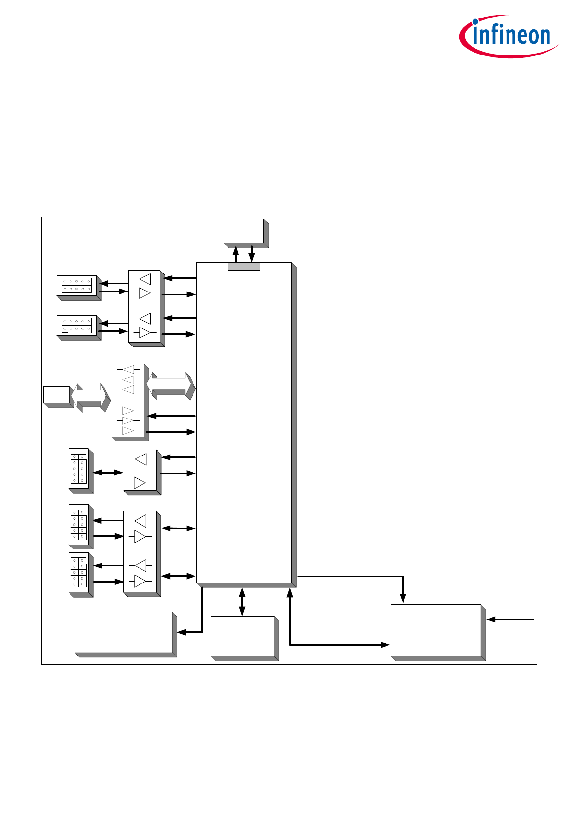
– Infineon’s TC3X3 (TC333, TC323) AURIX™ 2G Controller in TQFP-100 Package (0.4mm pitch)
–FlexRay™
– High Speed CAN Transceivers (CAN-FD capable)
– USB to UART bridge
–Serial Eeprom
–LIN Transceiver
– Crystal 20MHz (default) or External Clock
– USB miniWiggler JDS for easy debugging
– 8 Low Power Status LEDs
– 8-DIP switches for configuration
– access to all pins of controller
– 100mm x 160mm (EURO-Board)
1)
Transceivers
Connectors
The TC3X3 TriBoard offers a wide variety of connectors:
– Standard power connector
– Micro USB connector for ASC Interface (ASC0) and miniWiggler
– 16-pin header for JTAG interface (OCDS)
– 2 x 10-pin header for DAP and DAP_SCR
– 10pin (2x5) Header for LIN Transceiver (LIN)
– 2 x 10pin (2x5) Header for CAN High Speed Transceiver (CAN0 and CAN1)
– 2 x 10pin (2x5) Header for FlexRay™ (ERAY-A and ERAY-B)
– four 80-pin connectors (male) + four 80-pin connectors (female) with all I/O signals
– optional ETK connector
– optional 6pin (IEEE1394) Socket for HSCT
Components
– Infineon’s Multi Voltage Safety Micro Processor Supply TLF35584QV
– Three LEDs to validate power supply (5Volt / 3,3 Volt / 1,25 Volt)
– LED indicating safe state signal 2 from TLF35584
– LED indicating /HDRST (ESR0) active state
– LED indicating activ miniWiggler JDS
– LED switched via DAS software
– 2 x Infineon’s FlexRay™ Transceiver TLE9221SX
– 2 x Infineon’s High Speed CAN-Transceiver TLE9251VSJ
– Infineon’s LIN-Transceiver TLE 7259-3GE
– USB to UART bridge FT2232HL (FTDI)
– 8 general purpose LEDs
– 2K SPI Bus Serial Eeprom (MICROCHIP)
–Reset switch
–Enable switch
– Generic switch
1) FlexRay™ is a trademark of FlexRay Consortium.
User Manual 2-1 V1.0
TriBoard TC3X3 TH V1.0 and TriBoard TC3X3 V1.0 2020-05
Page 6
Micro
USB
miniWiggler
OCDS1
USB
XTAL
FlexRay
Transc eiver
Transc eiver
TxCAN03
TxCAN01
RxCAN03
RxCAN01
TC3X3
(e.g.
TC333,
TC323)
TriCore
TM
CPU
PLL
CAN0
CAN1
ERAY B ERAY A
TX0
RX0
8 LED s
(P20.10, P33.5 up to P33.7,
P20.11 up to P20.14)
Serial EEPROM
LIN
LIN
Transc eiver
TX1
RX1
QSPI1
WAKEUP
QSPI1
Multi Voltage Safety Micro
Processor Supply
TLF35584 QV
ENA
TriBoard Manual TC3X3
Hardware: TriBoard TC3X3 TH V1.0 and TriBoard TC3X3 V1.0
Features
– 4-pin Dip switch
Zero Ohm Bridges
Zero Ohm resistors give the flexibility to configure the systems functionality.
2.2 Block Diagram
Figure 2-1 TriBoard Block Schematic
User Manual 2-2 V1.0
TriBoard TC3X3 TH V1.0 and TriBoard TC3X3 V1.0 2020-05
Page 7
X402
X604
X406
X502
S202
R501
C501
C502
L501
L502
U501
D508
U502
S501
X501
X401
D504 D507
D506
D505
D309D308D307D306D305D304D303D302
X601
X602
X302 X301
T302
T301
U305
Y201
Y401
U401
D402
BU401
D401
C303
X303X304X305
S201
S502
X404
X603
U201
TriBoard Manual TC3X3
Hardware: TriBoard TC3X3 TH V1.0 and TriBoard TC3X3 V1.0
Features
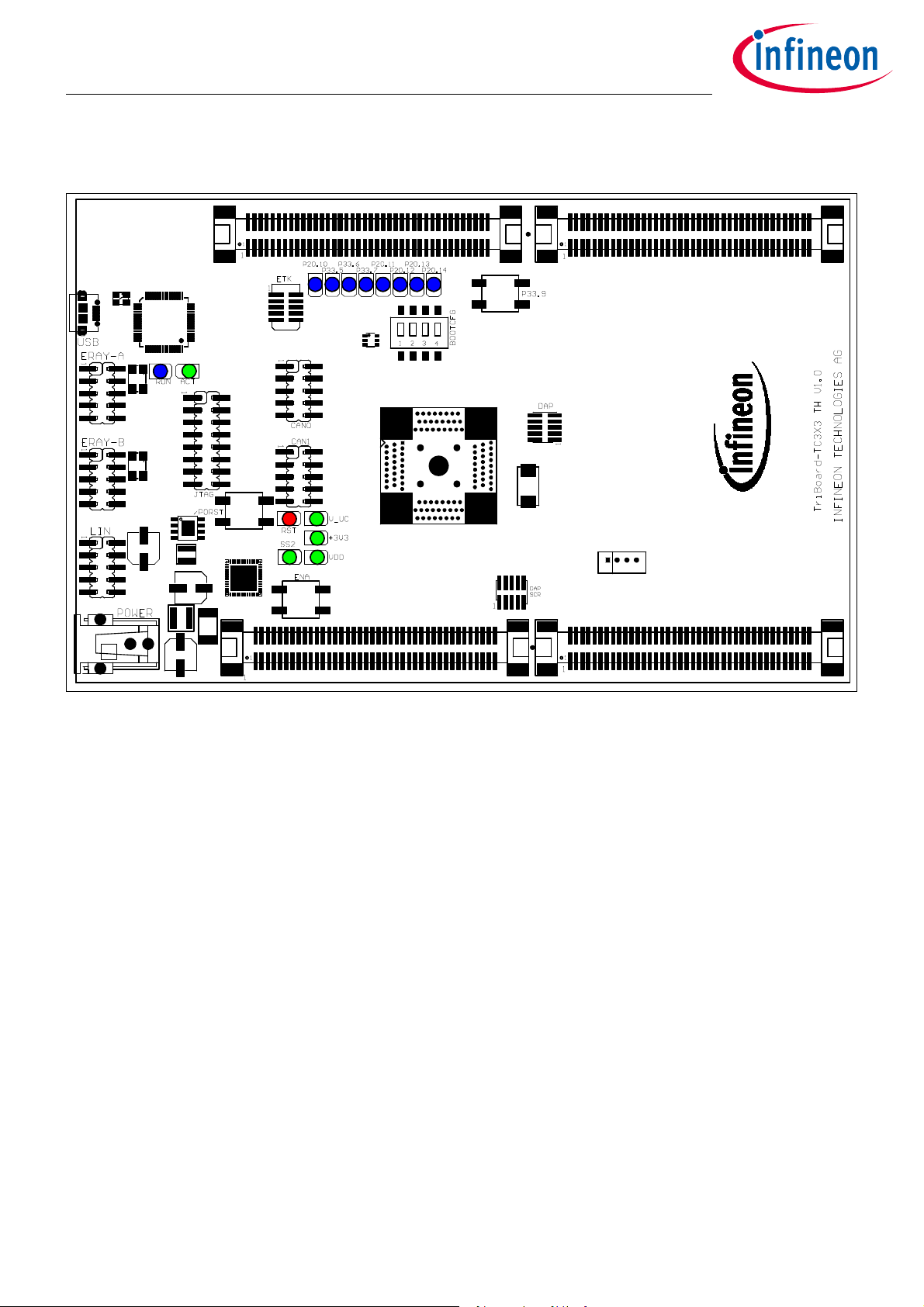
2.3 Placement
Figure 2-2
User Manual 2-3 V1.0
TriBoard TC3X3 TH V1.0 and TriBoard TC3X3 V1.0 2020-05
TriBoard TC3X3 (TH) V1.0 Placement
Page 8

TriBoard Manual TC3X3
Hardware: TriBoard TC3X3 TH V1.0 and TriBoard TC3X3 V1.0
TriBoard Information
3 TriBoard Information
3.1 Soldered board
TriBoard TC3X3 V1.0 is the soldered board and will be available only with usable devices. Please see also chapter
Usable devices.
3.2 Socketed board
TriBoard TC3X3 TH V1.0 is the socketed board.
3.2.1 Usable devices
Note: Note: Please check always the latest manual for complete list of usable/tested devices.
The board can be used with the following devices:
•TC333
• TC323 (planned, not yet tested)
3.2.2 Restricted usable devices
•None
3.3 Power Supply
All needed voltages are generated via Infineon’s Multi Voltage Safety Micro Processor Supply TLF35584QV and via
the microcontroller itself (+1,25V).
The supply device is available as two different devices:
TLF35584QVVS1 -> +5V standby voltage, +5V TriCore™ supply (V_UC)
TLF35584QVVS2 -> +3,3V standby voltage, +3,3V TriCore™ supply (V_UC)
Dependent of the assembled device the board works with 5V or 3,3V IO.
The TLF35584QV provide the following voltages:
+3,3V or +5V for standby (connected to VEVRSB)
+3,3V or +5V for TriCore™ (connected to VEXT)
+5V communcation supply (used by CAN and FlexRay™ transceivers)
+5V voltage reference (connected to VDDM and VAREFx)
+3,3V via LDO directly from pre regulator
Applying a stable supply voltage causes the power on reset after a short period. The three LED's (V_UC, +3.3V,
VDD) indicate the status of the on board generated voltages.
A manual power on reset is executed by pressing the reset button.
The Board has to be connected to a +3,5V to +40V DC power supply.
The power consumption is not specified yet but a supply with 12V and 500mA is recommended. The pinout for
the supply connector is shown in Figure 6-3. There can be used any standard power pack with a connector where
the positive line is surrounded by the ground line.
User Manual 3-1 V1.0
TriBoard TC3X3 TH V1.0 and TriBoard TC3X3 V1.0 2020-05
Page 9
R216
R213
R452
R429
R430
R214
R215
X402
R212
X604
R248
X406
R457
R346
X502
S202
R525
R348
R390
R256
R255
R241
R237
R235
R233
CB502
R509
R508
R507
R501
C504
C503
C501
C508
C509
C507
C502
CB501
L501
L502
U501
D508
C505
U502
CB510
R398
C519
R354
S501
X501
X401
D504 D507
D506
D505
D309
D308
D307
D306
D305
D304
D303
D302
X601
X602
X302 X301
T302 T 301
U305
R356
R355
R336
R335
R531
R439
C302 C301
R532
CB309
R396R394
R393R392
R391
R399
R324
R357 R337
Y201
R207
R206
C202
C201
R202
R203
CB204
R201
CB520
CB515
CB511
R428
R427
R426
R425
R424
R524
R344
CB402
R402
R403
CB408
Y401
U401
U404
CB401
R401
D402
L401
BU401
R411
C402
CB405
R423
D401
CB414
CB415
CB416
CB417
CB418
CB419
R444
R446
R454
R456
R455
R451
U406
U407
U408
C303
D301
R359
R361
R232
R234
R236
R240
X303X304X305
R205
R204
S201
R244
R245
R246
R249
CB205
R222
S502
X404
R395
C516
C517
R397
X603
U201
TriBoard Manual TC3X3
Hardware: TriBoard TC3X3 TH V1.0 and TriBoard TC3X3 V1.0
TriBoard Information
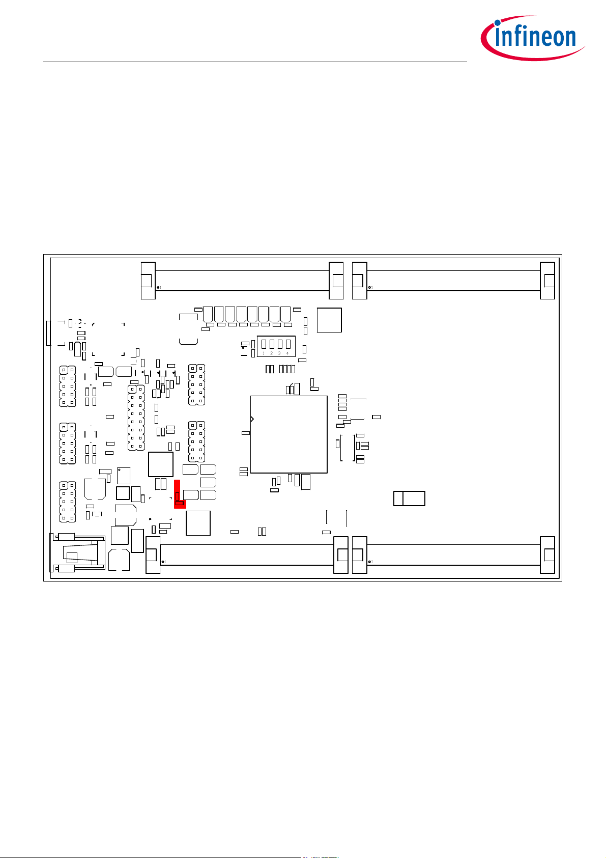
3.3.1 Failsafe handling
In case that the device don’t contains a program which disable or service the window watchdog and error pin
monitor of the TLF35584 then the TLF35584 is going to a FAILSAFE state where all supplies are switched off. This
state can be left via reconnect the power plug or via the ENA button (S502). In this case you must connect a
debugger which is able to disable the window watchdog and error pin monitor to reprogram the microcontroller.
In the default state of the board the switching to FAILSAFE state is switched off via resistor R508.
If you will use/evaluate all safety features of the TLF35584 make sure that R509 is assembled and R508 is not
assembled. Make sure that you have a proper initialization of TLF35584 in your softare.
Resistor R508 and R509 are red marked in the following Figure 3-1:
Figure 3-1 Resistors for TLF35584 Safety feature handling with switch on
3.4 LEDs
There are 15 LEDs on board:
– D302 up to D305 (blue) -> toogle LEDs connected to P22.10 and P33.5 ... P33.7
– D306 up to D309 (blue) -> toogle LEDs connected to P20.11 ... P20.14
– D504 RST (red) -> RESET LED indicate the reset state of the board (/ESR0)
– D505 VDD (green) ->VDD (+1,25V) power supply indication
– D506 +3V3 (green) -> +3,3V power supply indication
– D507 V_UC (green) -> +5V/+3,3V power supply indication
– D508 SS2 (green) -> safe state signal 2 indication
– D402 ACT (green) -> on board miniWiggler JDS is ACTIV
– D401 RUN (blue) -> Debug RUN mode (switched by DAS Server)
User Manual 3-2 V1.0
TriBoard TC3X3 TH V1.0 and TriBoard TC3X3 V1.0 2020-05
Page 10
CB409
R438
R437
R436
R312
R503
D502
C511
C512
D501
Q501
Q505
R506
R502
C510
R504
R505
D503
R520
R209
CB201
R320
R353
R352
R333
R334
R332
U304
U303
R351
R350
R358
R331
R330
R338
R304
R303
CB308
CB307
CB306
CB305
CB304
CB303
R342
R302
U302 U301
X701 X704
X702
Q503
Q504
Q502
R510
R512
R511
C515
R536
R535
R513
R534
R538
R317
R307
R537
CB518
CB516
CB51 2
CB302
CB301
R343
R323
R533
R221 R220
R322
R321
R340
R341
R311
R301
R319
R318
R316
R315
R309
R308
R306
R305
CB404
CB406
R405
R406
U402
R407
CB40 3
CB407
R409
R410
R415
R416
R417
R418
R414
R420
C406
R412
Q401
Q402
U403
R421
R422
C404
C405
CB410
CB411
CB412
R441
R442
R450
C401
R404
D403
C403
CB413
L402
U405
R413
R443
R445
R447
R448
R449
C304
CB310
R360
R362
R363
R364
R365
R521
U306
R408
R208
CB202
R431
R433
C203
C204
C205
C207
C208
Q403
R440
R419
C518
CB517
X703
TriBoard Manual TC3X3
Hardware: TriBoard TC3X3 TH V1.0 and TriBoard TC3X3 V1.0
TriBoard Information
3.5 Clock
On the board is a fixed crystal with 20MHz assembled. You can change this by replacing Y101 (soldered).
3.6 USB Connector
The USB connector is used for connection to a PC. Via the USB it is possible to power the board, using the ASCLIN0
as serial connection via USB and Debugging via DAS. For the pinout of USB socket see Figure 6-4.
NOTE: Before connecting the board to the PC, make sure that the actual DAS software is installed on the PC. For
actual DAS software please contact your local FAE.
The software can also be found on:
DAS website
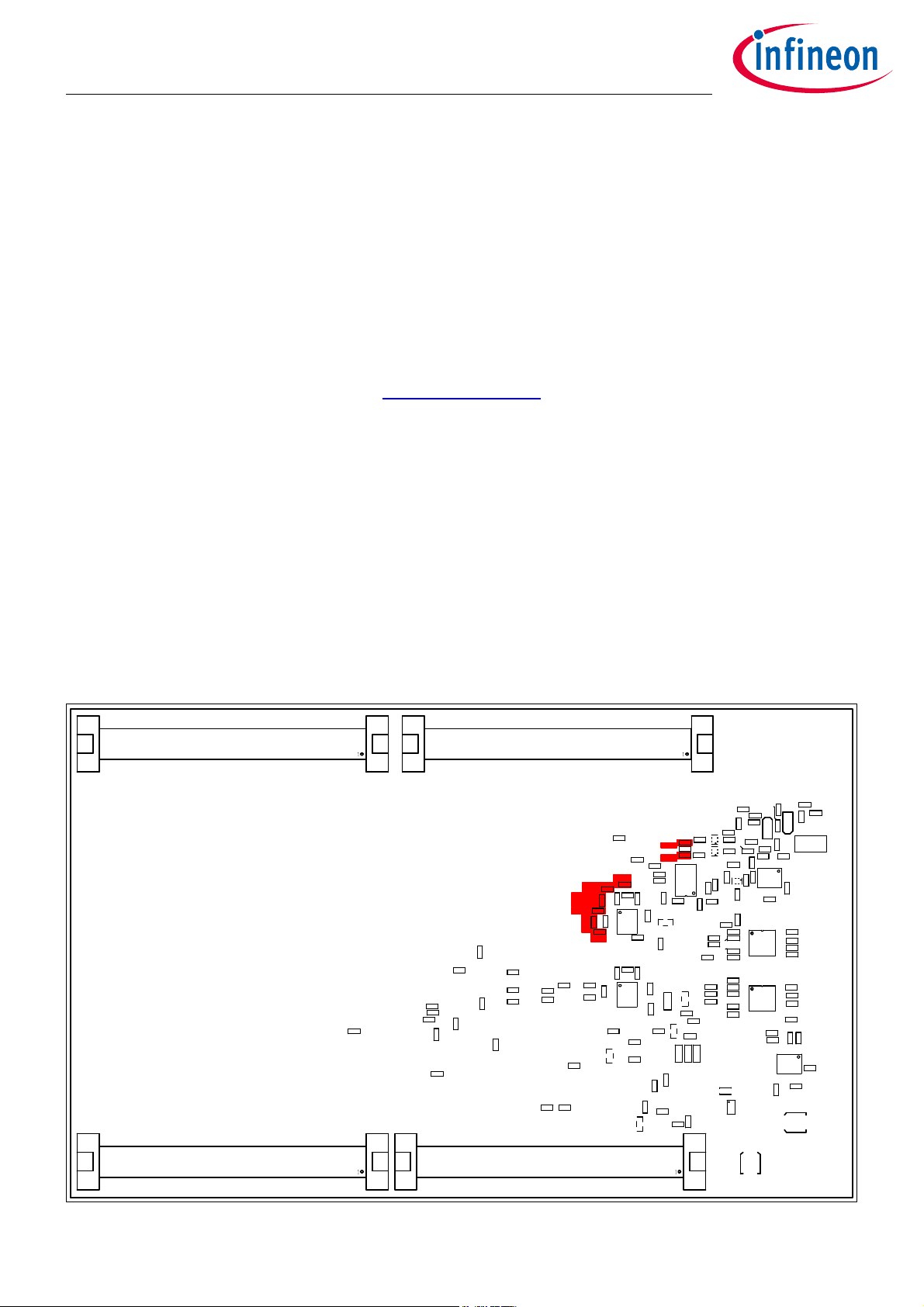
3.6.1 Serial Connection to PC
After the first connection of USB to a PC the needed driver will be installed automatically. During this there will
be created a new COM port on PC. This COM port can be used to communicate with the board via ASCLIN0 of the
device. Per default the ASCLIN0 is used on P14.0 and P14.1 (e.g. Generic Bootstrap Loader) . In case you will use
the Generic Bootstrap Loader via CAN or ASCLIN0 via P15.2 and P15.3 you must:
– remove R436 and R437 (this disconnect the serial connection from P14.0 and P14.1)
– remove R301 and R302 (this disconnect the CAN0 transceiver from P11.10 and P11.12)
– assemble R438 and R440 with 0R resistor (size 0603) to connect P15.2 and P15.3 to serial connection
– assemble R303 and R304 with 0R resistor (size 0603) to connect P14.0 and P14.1 to CAN0 transceiver
The mentioned resistors are red marked in Figure 3-2.
Figure 3-2 Resistors for ASC connection (ASC0)
User Manual 3-3 V1.0
TriBoard TC3X3 TH V1.0 and TriBoard TC3X3 V1.0 2020-05
Page 11

TriBoard Manual TC3X3
Hardware: TriBoard TC3X3 TH V1.0 and TriBoard TC3X3 V1.0
TriBoard Information
3.6.2 miniWiggler JDS
The miniWiggler JDS is a low cost debug tool which allows you access to the JTAG of the device. Make sure that
you have the latest DAS release. Debugging is possible via the DAS Server ‘UDAS‘. Please contact your prefered
debug vendor for support of DAS.
If you have connected the board to the PC and there runs the DAS server, then a working connection is visible via
the green ACTIV LED.
The status RUN LED is switched on/off through the DAS Server, depending on the used debugger (client).
IMPORTANT: Make sure that there is no or a tristated connection on X401 (OCDS1) and X402 (DAP) if the
ACTIV LED is on.
Per default the miniWiggler is connected to the DAP. If resistors R214, R215 and R216 assembled (default) then
the standard DAP is connected to miniWiggler. If all this resistors are not assembled then the miniWiggler can’t
be used. In this case only the DAP connectors X402 and X406 can be used. See Figure 3-6.
3.7 FlexRay™ (E-RAY)
The board has 2 IDC10 plugs for FlexRay™ Communication (channel A and B) with up to 10 Mbit/s. For the pinout
of the plugs see Figure 6-5. You can use a IDC female connector with crimpconnector, flat cable and SUB-D 9 plug
with crimpconnector to have a 1:1 adapter to SUB-D 9.
The transceiver are connected to the TriCore™ device via zero ohm resistors (R320 up to R324 and R340 up to
R344) which must be removed to use the ports outside.
ERAY-A can be connected to P02.0, P02.1 and P02.4. Transceiver for channel A can be enabled/disabled via P20.8.
The error state of transceiver channel A can be read out via P20.9.
ERAY-B is connected to P02.2, P02.3 and P02.5. Transceiver for channel B can be enabled/disabled via P02.6. The
error state of transceiver channel A can be read out via P02.7.
For more information look in the user manual for TC3X3 TQFP.
3.8 Serial EEPROM
The QSPI1 of the TC3X3 TQFP is connected to a serial EEPROM with a size of 2KBit (256 x 8). As chip select for this
EEPROM is used the port pin P23.1. P23.1 has no chip select functionality of QSPI. Therefore the software must
generate the chip select manual via bit banging. To disconnect (disable) the EEPROM remove resistor R348.
3.9 MultiCAN
On the board are two CAN transceiver connected to the CAN0 and CAN1 of TC3X3 TQFP. The transceivers are
connected to two IDC10 plug. For the pinout of IDC10 plug see Figure 6-6. You can use a IDC female connector
with crimpconnector, flat cable and SUB-D 9 plug with crimpconnector to have a 1:1 adapter to SUB-D 9.
The transceiver are connected to the TriCore™ device via zero ohm resistors (R301 up to R304 and R311 up to
R314) which must be removed to use the ports outside.
CAN0 can be used via P11.10 and P11.12 (CAN0 node 3, default) or P14.0 and P14.1 (CAN0 node 1). CAN1 can be
used via P15.2 and P15.3 (CAN0 node 1, default).
3.10 LIN
On the board is one LIN transceiver connected to the ASCLIN1 on TC3X3 TQFP (P15.0 and P15.1). The transceiver
are connected to one IDC10 plug. For the pinout of IDC10 plug see Figure 6-7. You can use a IDC female connector
with crimpconnector, flat cable and SUB-D 9 plug with crimpconnector to have a 1:1 adapter to SUB-D 9.
To disconnect the LIN remove resistor R364 and R365.
User Manual 3-4 V1.0
TriBoard TC3X3 TH V1.0 and TriBoard TC3X3 V1.0 2020-05
Page 12
CB409
R438
R437
R436
R312
R503
D502
C511
C512
D501
Q501
Q505
R506
R502
C510
R504
R505
D503
R520
R209
CB201
R320
R353
R352
R333
R334
R332
U304
U303
R351
R350
R358
R331
R330
R338
R304
R303
CB308
CB307
CB306
CB305
CB304
CB303
R342
R302
U302 U301
X701 X704
X702
Q503
Q504
Q502
R510
R512
R511
C515
R536
R535
R513
R534
R538
R317
R307
R537
CB518
CB516
CB51 2
CB302
CB301
R343
R323
R533
R221 R220
R322
R321
R340
R341
R311
R301
R319
R318
R316
R315
R309
R308
R306
R305
CB404
CB406
R405
R406
U402
R407
CB40 3
CB407
R409
R410
R415
R416
R417
R418
R414
R420
C406
R412
Q401
Q402
U403
R421
R422
C404
C405
CB410
CB411
CB412
R441
R442
R450
C401
R404
D403
C403
CB413
L402
U405
R413
R443
R445
R447
R448
R449
C304
CB310
R360
R362
R363
R364
R365
R521
U306
R408
R208
CB202
R431
R433
C203
C204
C205
C207
C208
Q403
R440
R419
C518
CB517
X703
TriBoard Manual TC3X3
Hardware: TriBoard TC3X3 TH V1.0 and TriBoard TC3X3 V1.0
TriBoard Information
The LIN can be used in master and in slave mode. For the master mode there is per default a pull-up of 1K (R360)
and a capacitor of 1nF (C304) on the BUS assembled. For using the LIN in slave mode the pull-up resistor R360
must be removed and maybe the capacitor changed to a smaller value (e.g. 220pF).
The mentioned resistor and capacitor are red marked in Figure 3-3
Figure 3-3 Components for LIN Master Mode
3.11 ADC
On this boards are 5 ADC channels prepared with a low pass filter. On pin AN5, AN11, AN12, AN32 and AN33 is
assembled a capacitor of 47nF and a serial resistor of 4,7K. The filter components are red marked in the following
figures (Figure 3-4 and Figure 3-5).
User Manual 3-5 V1.0
TriBoard TC3X3 TH V1.0 and TriBoard TC3X3 V1.0 2020-05
Page 13
R216
R213
R452
R429
R430
R214
R215
X402
R212
X604
R248
X406
R457
R346
X502
S202
R525
R348
R390
R256
R255
R241
R237
R235
R233
CB502
R509
R508
R507
R501
C504
C503
C501
C508
C509
C507
C502
CB501
L501
L502
U501
D508
C505
U502
CB510
R398
C519
R354
S501
X501
X401
D504 D507
D506
D505
D309
D308
D307
D306
D305
D304
D303
D302
X601
X602
X302 X301
T302 T301
U305
R356
R355
R336
R335
R531
R439
C302 C301
R532
CB309
R396R394
R393R392
R391
R399
R324
R357 R337
Y201
R207
R206
C202
C201
R202
R203
CB204
R201
CB520
CB515
CB511
R428
R427
R426
R425
R424
R524
R344
CB402
R402
R403
CB408
Y401
U401
U404
CB401
R401
D402
L401
BU401
R411
C402
CB405
R423
D401
CB414
CB415
CB416
CB417
CB418
CB419
R444
R446
R454
R456
R455
R451
U406
U407
U408
C303
D301
R359
R361
R232
R234
R236
R240
X303X304X305
R205
R204
S201
R244
R245
R246
R249
CB205
R222
S502
X404
R395
C516
C517
R397
X603
U201
CB409
R438
R437
R436
R312
R503
D502
C511
C512
D501
Q501
Q505
R506
R502
C510
R504
R505
D503
R520
R209
CB201
R320
R353
R352
R333
R334
R332
U304
U303
R351
R350
R358
R331
R330
R338
R304
R303
CB308
CB307
CB306
CB305
CB304
CB303
R342
R302
U302 U301
X701 X704
X702
Q503
Q504
Q502
R510
R512
R511
C515
R536
R535
R513
R534
R538
R317
R307
R537
CB518
CB516
CB51 2
CB302
CB301
R343
R323
R533
R221 R220
R322
R321
R340
R341
R311
R301
R319
R318
R316
R315
R309
R308
R306
R305
CB404
CB406
R405
R406
U402
R407
CB40 3
CB407
R409
R410
R415
R416
R417
R418
R414
R420
C406
R412
Q401
Q402
U403
R421
R422
C404
C405
CB410
CB411
CB412
R441
R442
R450
C401
R404
D403
C403
CB413
L402
U405
R413
R443
R445
R447
R448
R449
C304
CB310
R360
R362
R363
R364
R365
R521
U306
R408
R208
CB202
R431
R433
C203
C204
C205
C207
C208
Q403
R440
R419
C518
CB517
X703
TriBoard Manual TC3X3
Hardware: TriBoard TC3X3 TH V1.0 and TriBoard TC3X3 V1.0
TriBoard Information
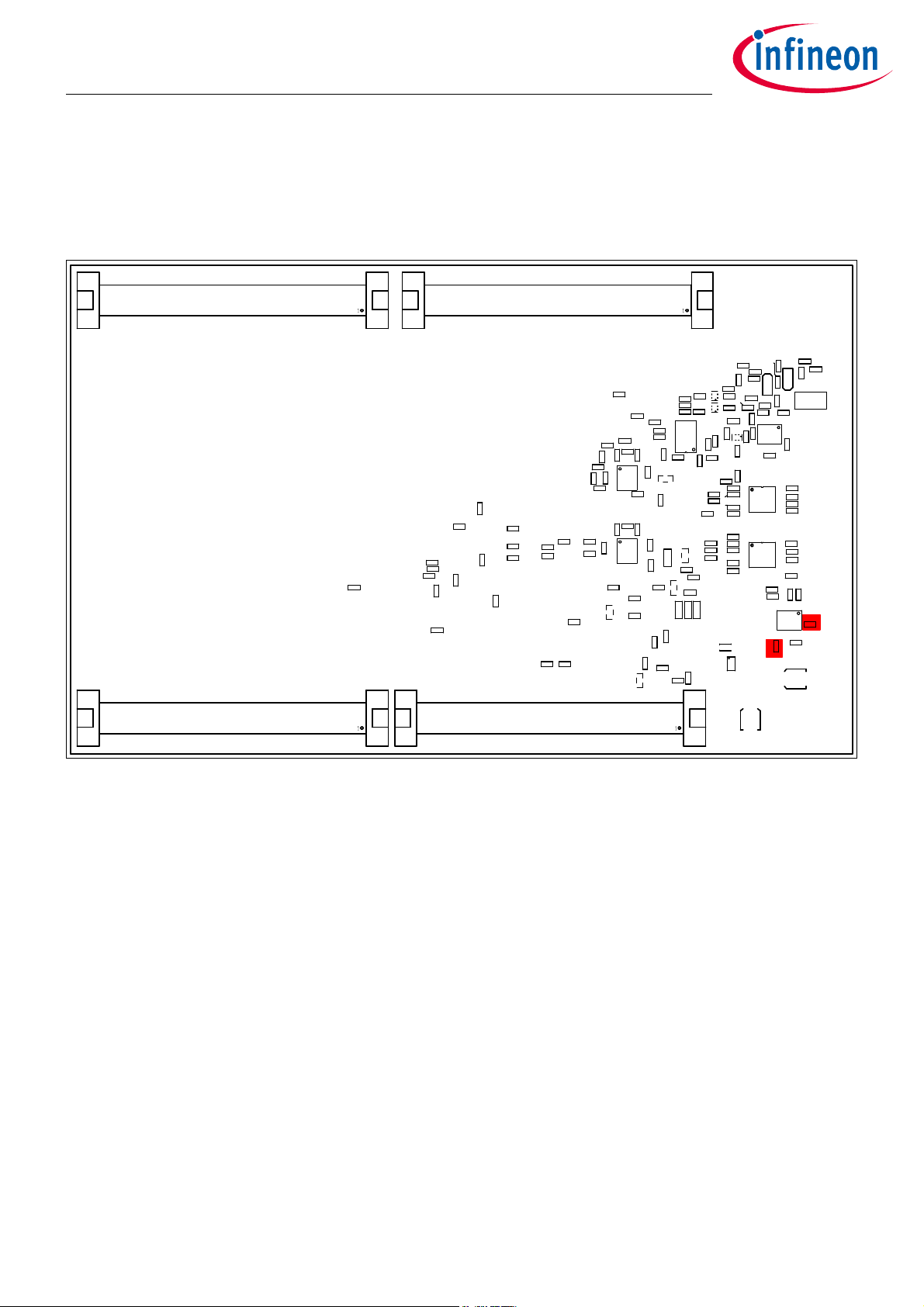
Figure 3-4 Filter components of ADC channels on Top Side
Figure 3-5 Filter components of ADC channels on Bottom Side
User Manual 3-6 V1.0
TriBoard TC3X3 TH V1.0 and TriBoard TC3X3 V1.0 2020-05
Page 14

TriBoard Manual TC3X3
Hardware: TriBoard TC3X3 TH V1.0 and TriBoard TC3X3 V1.0
TriBoard Information
3.12 Other peripherals
For all other peripherals there are no special plugs on the board. The peripheral signals are available on the
different connectors. See “Connector Pin Assignment” on Page 6-1.
3.13 Toggle LED’s
The status LED’s are low active and can be controlled by Software.
Port 20 pin 11 up to pin 14 are connected to single LED’s (D306... D309) and powered by the normal
microcontroller voltage.
Port 20 pin 10 and Port 33 pin 5 up to pin 7 are connected to single LED’s (D302... D305) and powered by the
standby voltage. This means that this LED’s can be are activ also when the board is in standby mode and only the
standby voltage available (port 33 is powered by VEVRSB pin which is connected to standby supply of TLF35584).
In this case the port pins are controlled by the standby controller if available.
Note: LED on P20.10 (D302) is always on if only VEVRSB is supplied.
3.14 Buttons
On the board are three buttons.
The reset button (S501) will apply a warm power on reset to the device.
The ENA button (S502) will be used to enable/wakeup the TLF35584.
The P33.9 button (S202) can be used by software as input. Also can this button used by the standby controller to
react on an event when only standby supply is available (e.g. wakeup the TLF35584 via P33.10).
3.15 Debug System
3.15.1 OCDS1
The OCDS1 signals are connected to the IDC16 plug (X401). They work with the port supply of Microcontroller (+5V
default or +3,3V). For pinout of the connector see Figure 6-8. You can connect any debugger to this connector.
The signals /BRKIN and /BRKOUT are not connected per default. If you need this signals in the connector then
assemble R424 and R425 or R426 with a 0R resistor.
If you connect a debug hardware make sure that the miniWiggler JDS (see “miniWiggler JDS” on Page 3-4) is not
activ (ACTIV LED is off) and on the DAP connector (X402) is no hardware connected or the hardware is tristated.
If the ACTIV LED is on, then stop the active DAS Server ’UDAS’ and/or remove the USB connection to the PC.
If R214 up to R216 not assembled then the connector is not usable.
3.15.2 DAP
The board comes with a DAP connector (X402). For pinout of this connector see Figure 6-9. You can connect a DAP
hardware here. If you use this connector make sure that the miniWiggler JDS is not activ (ACTIV LED is off) and a
connected OCDS1 hardware is disconnected or tristated.
3.15.3 DAP_SCR
Additional DAP connector (X406) is connected to DAP_SCR. This DAP can be used as private DAP connection to
the standby controller. For pinout of this connector see Figure 6-9. You can connect a DAP hardware here. This
DAP use P33.6 and P33.7 which are connected to LED on the board. Maybe it is necessary to remove R393 and
R394 if the speed of the connection is not fast enough.
User Manual 3-7 V1.0
TriBoard TC3X3 TH V1.0 and TriBoard TC3X3 V1.0 2020-05
Page 15

R216
R213
R452
R429
R430
R214
R215
X402
R212
X604
R248
X406
R457
R346
X502
S202
R525
R348
R390
R256
R255
R241
R237
R235
R233
CB502
R509
R508
R507
R501
C504
C503
C501
C508
C509
C507
C502
CB501
L501
L502
U501
D508
C505
U502
CB510
R398
C519
R354
S501
X501
X401
D504 D507
D506
D505
D309
D308
D307
D306
D305
D304
D303
D302
X601
X602
X302 X30 1
T302 T301
U305
R356
R355
R336
R335
R531
R439
C302 C301
R532
CB309
R396R394
R393R392
R391
R399
R324
R357 R337
Y201
R207
R206
C202
C201
R202
R203
CB204
R201
CB520
CB515
CB511
R428
R427
R426
R425
R424
R524
R344
CB402
R402
R403
CB408
Y401
U401
U404
CB401
R401
D402
L401
BU401
R411
C402
CB405
R423
D401
CB414
CB415
CB416
CB417
CB418
CB419
R444
R446
R454
R456
R455
R451
U406
U407
U408
C303
D301
R359
R361
R232
R234
R236
R240
X303X304X305
R205
R204
S201
R244
R245
R246
R249
CB205
R222
S502
X404
R395
C516
C517
R397
X603
U201
TriBoard Manual TC3X3
Hardware: TriBoard TC3X3 TH V1.0 and TriBoard TC3X3 V1.0
TriBoard Information
3.15.4 High speed with DAP
For use the DAP connection with 160 MHz you need to remove 3 resistors to have a very short connection between
device and connector. On the TC3X3 Triboard this 3 resistors are R214, R215 and R216 for DAP (red marked in
Figure 3-6). This resistors needs to be removed.
Important: When the re sistors are removed then only the D AP connector on th e board can be used . The on board
wiggler and the OCDS1 co nnector couldn’t be use (ar e disconnected) in this case, also the DAP/JTAG part of the
ETK connector couldn’t be used.
All resistors are red marked in the following figure:
Figure 3-6 Location of DAP resistors on Top Side
3.15.5 ETK connector (optional)
The TriBoard provide a 10 pin samtec connector (X404) for connecting to an ETK. This connector should be
assembled by your self if needed.
For the pinout of connector see Figure 6-10.
The needed Samtec connector is: TFM-105-02-A.
3.15.6 EmW Power (optional)
The TriBoard provide the 4 pin power connector (X502) for the Ethernet miniWiggler (EmW). This connector
should be assembled by your self if needed.
For the pinout of connector see Figure 6-11.
The needed Samtec connector is the JST B4B-PH-K.
The connector provide the input voltage to the Ethernet miniWiggler and an enable/wakeup signal connected to
TLF35584.
User Manual 3-8 V1.0
TriBoard TC3X3 TH V1.0 and TriBoard TC3X3 V1.0 2020-05
Page 16

TriBoard Manual TC3X3
Hardware: TriBoard TC3X3 TH V1.0 and TriBoard TC3X3 V1.0
TriBoard Information
Because the device don’t have a VDDSB pin the 1,25V standby supply pin of the connector is not connected on
this board.
User Manual 3-9 V1.0
TriBoard TC3X3 TH V1.0 and TriBoard TC3X3 V1.0 2020-05
Page 17

2
on
134
P
1
0
.
5
P
1
0
.
6
P
1
4
.
3
TriBoard Manual TC3X3
Hardware: TriBoard TC3X3 TH V1.0 and TriBoard TC3X3 V1.0
TriBoard Configuration
4 TriBoard Configuration
4.1 HW Boot Configuration
Figure 4-1 HW Configuration DIP-Switches
The picture above shows the definition of the boot HW configuration switch. The meaning of the switches will be
described in the following table (Table 4-1).
Note:
The ON position of the switch is equal to a logical LOW at the dedicated pin.
4.1.1 Default Pad State
P14.4 / HWCFG6 is not bonded at this package. Therefore the pin is ‘open’ and the internal pull-up is active. This
means the Default Pad State is always that the internal pull-ups are enabled.
4.1.2 Bootmode
Table 4-1 User Startup Modes
HWCFG[5...3] Type of Boot 2 3 4
XX1 Start-up mode is selected by Boot Mode Index X X OFF
110 Internal Start from Flash OFF OFF ON
100 Alternate Boot Mode, Generic Bootstrap Loader on fail (P14.0/P14.1) ON OFF ON
010 Alternate Boot Mode, ASC Bootstrap Loader on fail (P15.2/P15.3) OFF ON ON
000 Generic Bootstrap Loader (P14.0/P14.1) ON ON ON
1) The shadowed line indicates the default setting.
2) ’x’ represents the don’t care state.
3) 2 to 4 are the Dip Switch numbers.
1)2)3)
User Manual 4-1 V1.0
TriBoard TC3X3 TH V1.0 and TriBoard TC3X3 V1.0 2020-05
Page 18

TriBoard Manual TC3X3
Hardware: TriBoard TC3X3 TH V1.0 and TriBoard TC3X3 V1.0
TriBoard Configuration
4.2 Assembly Options
4.2.1 General optional resistors
Table 4-2 General optional resistors (default assembly in brackets)
Component Description
R202 Connect P20.2 (/TESTMODE) to GND (not assembled)
R203 XTAL1 Rload (50 Ohm) (not assembled)
R206 XTAL Rparallel (not assembled)
R207 XTAL2 Rserial (assembled)
R238 Switch off EVRC (not assembled)
R240 Switch off EVR33 (not assembled)
R390 Connect V_STBY to toggle LEDs D302...D305 (assembled)
R399 Connect V_UC to toggle LEDs D306...D309 (assembled)
R423 Connect P20.0 with miniWiggler JDS (not assembled)
R424 Connect P20.0 with OCDS1 connector (not assembled)
R425 Connect P21.7 with OCDS1 connector (not assembled)
R426 Connect P20.2 with OCDS1 connector (not assembled)
R427 Connect P21.7 with USR1 of miniWiggler JDS (not assembled)
R428 Connect P20.2 with USR1 of miniWiggler JDS (not assembled)
R429 Connect P21.6 (DAP3) with USR1 of DAP (assembled)
R430 Connect P20.2 with USR1 of DAP (not assembled)
R433 Connect P21.7 with ETK connector (not assembled)
R439 Connect P21.7 with ETK connector (not assembled)
R508 Connect pin MPS of TLF35584 to V_CO (not assembled)
R509 Connect pin MPS of TLF35584 to Ground (assembled)
R524 Connect VDDP3 to V_UC (not assembled)
R525 Connect VDDP3 to +3V3 (not assembled)
Note: All resistors are red marked in the following figures
User Manual 4-2 V1.0
TriBoard TC3X3 TH V1.0 and TriBoard TC3X3 V1.0 2020-05
Page 19

R216
R213
R452
R429
R430
R214
R215
X402
R212
X604
R248
X406
R457
R346
X502
S202
R525
R348
R390
R256
R255
R241
R237
R235
R233
CB502
R509
R508
R507
R501
C504
C503
C501
C508
C509
C507
C502
CB501
L501
L502
U501
D508
C505
U502
CB510
R398
C519
R354
S501
X501
X401
D504 D507
D506
D505
D309
D308
D307
D306
D305
D304
D303
D302
X601
X602
X302 X301
T302 T301
U305
R356
R355
R336
R335
R531
R439
C302 C301
R532
CB309
R396R394
R393R392
R391
R399
R324
R357 R337
Y201
R207
R206
C202
C201
R202
R203
CB204
R201
CB520
CB515
CB511
R428
R427
R426
R425
R424
R524
R344
CB402
R402
R403
CB408
Y401
U401
U404
CB401
R401
D402
L401
BU401
R411
C402
CB405
R423
D401
CB414
CB415
CB416
CB417
CB418
CB419
R444
R446
R454
R456
R455
R451
U406
U407
U408
C303
D301
R359
R361
R232
R234
R236
R240
X303X304X305
R205
R204
S201
R244
R245
R246
R249
CB205
R222
S502
X404
R395
C516
C517
R397
X603
U201
CB409
R438
R437
R436
R312
R503
D502
C511
C512
D501
Q501
Q505
R506
R502
C510
R504
R505
D503
R520
R209
CB201
R320
R353
R352
R333
R334
R332
U304
U303
R351
R350
R358
R331
R330
R338
R304
R303
CB308
CB307
CB306
CB305
CB304
CB303
R342
R302
U302 U301
X701 X704
X702
Q503
Q504
Q502
R510
R512
R511
C515
R536
R535
R513
R534
R538
R317
R307
R537
CB518
CB516
CB51 2
CB302
CB301
R343
R323
R533
R221 R220
R322
R321
R340
R341
R311
R301
R319
R318
R316
R315
R309
R308
R306
R305
CB404
CB406
R405
R406
U402
R407
CB40 3
CB407
R409
R410
R415
R416
R417
R418
R414
R420
C406
R412
Q401
Q402
U403
R421
R422
C404
C405
CB410
CB411
CB412
R441
R442
R450
C401
R404
D403
C403
CB413
L402
U405
R413
R443
R445
R447
R448
R449
C304
CB310
R360
R362
R363
R364
R365
R521
U306
R408
R208
CB202
R431
R433
C203
C204
C205
C207
C208
Q403
R440
R419
C518
CB517
X703
TriBoard Manual TC3X3
Hardware: TriBoard TC3X3 TH V1.0 and TriBoard TC3X3 V1.0
TriBoard Configuration
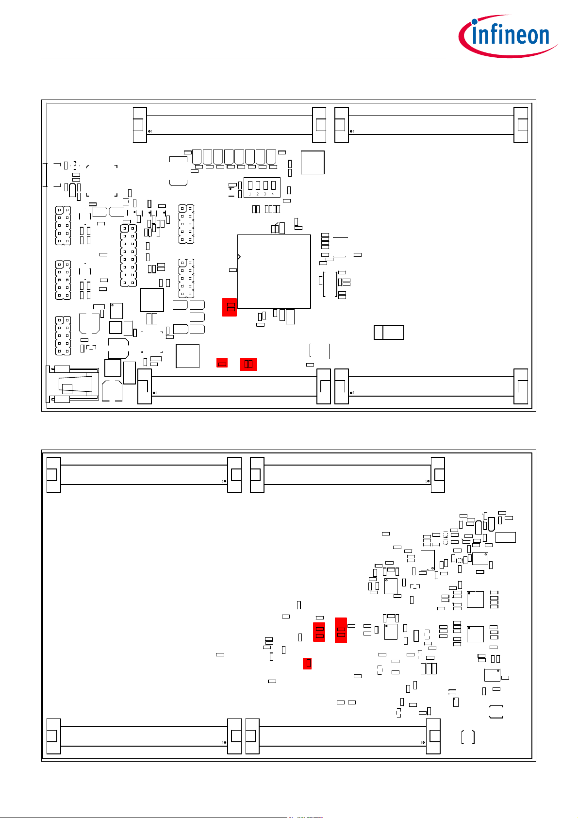
Figure 4-2 Location of general optional resistors on Top Side
Figure 4-3 Location of general optional resistors on Bottom Side
User Manual 4-3 V1.0
TriBoard TC3X3 TH V1.0 and TriBoard TC3X3 V1.0 2020-05
Page 20

TriBoard Manual TC3X3
Hardware: TriBoard TC3X3 TH V1.0 and TriBoard TC3X3 V1.0
TriBoard Configuration
4.2.2 Resistors for peripherals
Table 4-3 Resistors for peripherals (default assembly in brackets)
Component Description
R220 Connect V_VR with VDDM (assembled)
R221 Connect +3V3 with VDDM (not assembled)
R222 Connect VAREF1 with VDDM (assembled)
R301 Connect P11.10 with RXD of CAN0 transceiver (assembled)
R302 Connect P11.12 with TXD of CAN0 transceiver (assembled)
R303 Connect P14.1 with RXD of CAN0 transceiver (not assembled)
R304 Connect P14.0 with TXD of CAN0 transceiver (not assembled)
R311 Connect P15.3 with RXD of CAN1 transceiver (assembled)
R312 Connect P15.2 with TXD of CAN1 transceiver (assembled)
R320 Connect P02.0 with TXD of ERAY-A transceiver (assembled)
R321 Connect P02.4 with TXDEN of ERAY-A transceiver (assembled)
R322 Connect P02.1 with RXD of ERAY-A transceiver (assembled)
R323 Connect P20.8 with EN of ERAY-A transceiver (assembled)
R324 Connect P20.9 with ERRN of ERAY-A transceiver (assembled)
R340 Connect P02.2 with TXD of ERAY-B transceiver (assembled)
R341 Connect P02.5 with TXDEN of ERAY-B transceiver (assembled)
R342 Connect P02.3 with RXD of ERAY-B transceiver (assembled)
R343 Connect P02.6 with EN of ERAY-B transceiver (assembled)
R344 Connect P02.7 with ERRN of ERAY-B transceiver (assembled)
R348 Connect P23.1 with CS of SPI Eeprom (assembled)
R364 Connect P15.1 with RXD of LIN1 transceiver (assembled)
R365 Connect P15.0 with TXD of LIN1 transceiver (assembled)
R436 Connect P14.0 with RXD of USB to UART (assembled)
R437 Connect P14.1 with TXD of USB to UART (assembled)
R438 Connect P15.2 with RXD of USB to UART (not assembled)
R440 Connect P15.3 with TXD of USB to UART (not assembled)
Note: All resistors are red marked in the following figures
User Manual 4-4 V1.0
TriBoard TC3X3 TH V1.0 and TriBoard TC3X3 V1.0 2020-05
Page 21

R216
R213
R452
R429
R430
R214
R215
X402
R212
X604
R248
X406
R457
R346
X502
S202
R525
R348
R390
R256
R255
R241
R237
R235
R233
CB502
R509
R508
R507
R501
C504
C503
C501
C508
C509
C507
C502
CB501
L501
L502
U501
D508
C505
U502
CB510
R398
C519
R354
S501
X501
X401
D504 D507
D506
D505
D309
D308
D307
D306
D305
D304
D303
D302
X601
X602
X302 X301
T302 T301
U305
R356
R355
R336
R335
R531
R439
C302 C301
R532
CB309
R396R394
R393R392
R391
R399
R324
R357 R337
Y201
R207
R206
C202
C201
R202
R203
CB204
R201
CB520
CB515
CB511
R428
R427
R426
R425
R424
R524
R344
CB402
R402
R403
CB408
Y401
U401
U404
CB401
R401
D402
L401
BU401
R411
C402
CB405
R423
D401
CB414
CB415
CB416
CB417
CB418
CB419
R444
R446
R454
R456
R455
R451
U406
U407
U408
C303
D301
R359
R361
R232
R234
R236
R240
X303X304X305
R205
R204
S201
R244
R245
R246
R249
CB205
R222
S502
X404
R395
C516
C517
R397
X603
U201
CB409
R438
R437
R436
R312
R503
D502
C511
C512
D501
Q501
Q505
R506
R502
C510
R504
R505
D503
R520
R209
CB201
R320
R353
R352
R333
R334
R332
U304
U303
R351
R350
R358
R331
R330
R338
R304
R303
CB308
CB307
CB306
CB305
CB304
CB303
R342
R302
U302 U301
X701 X704
X702
Q503
Q504
Q502
R510
R512
R511
C515
R536
R535
R513
R534
R538
R317
R307
R537
CB518
CB516
CB51 2
CB302
CB301
R343
R323
R533
R221 R220
R322
R321
R340
R341
R311
R301
R319
R318
R316
R315
R309
R308
R306
R305
CB404
CB406
R405
R406
U402
R407
CB40 3
CB407
R409
R410
R415
R416
R417
R418
R414
R420
C406
R412
Q401
Q402
U403
R421
R422
C404
C405
CB410
CB411
CB412
R441
R442
R450
C401
R404
D403
C403
CB413
L402
U405
R413
R443
R445
R447
R448
R449
C304
CB310
R360
R362
R363
R364
R365
R521
U306
R408
R208
CB202
R431
R433
C203
C204
C205
C207
C208
Q403
R440
R419
C518
CB517
X703
TriBoard Manual TC3X3
Hardware: TriBoard TC3X3 TH V1.0 and TriBoard TC3X3 V1.0
TriBoard Configuration
Figure 4-4 Location of peripheral resistors on Top Side
Figure 4-5 Location of peripheral resistors on Bottom Side
User Manual 4-5 V1.0
TriBoard TC3X3 TH V1.0 and TriBoard TC3X3 V1.0 2020-05
Page 22

TriBoard Manual TC3X3
Hardware: TriBoard TC3X3 TH V1.0 and TriBoard TC3X3 V1.0
Signal (on board used) Description
5 Signal (on board used) Description
For more information about the signals please see the user manual/datasheet for TC3X3 and/or the schematics
of the board.
All not mentioned signals are not used on the board and can be used outside. Optional marked signals are used
only if they are connected (default is that they are not used on the board).
5.1 Power Signals
Table 5-1 Power Signals
Short name Description
VCC_IN Supply Input (3,5V...40V)
VIN Input Voltage of Power Supply Device
GND Ground
V_PREPEG Pre Regulator Voltage (~5,8V)
V_UC Microcontroller Supply Voltage (5V or 3,3V depends on assembled TLF35584)
V_CO Communication Supply Voltage (5V)
V_VR Reference Supply Voltage (5V)
V_STBY Standby Supply Voltage (5V or 3,3V depends on assembled TLF35584)
VDD Core Supply Voltage (1,25V)
VDDSB Emulation Stand-by SRAM Supply Voltage (1,25V)
VDDP3 Flash Power Supply Voltage (3,3V)
VFLEX Flexport Supply Voltage (3,3V)
VEXTOSC Oscillator Port Supply Voltage (5V or 3,3V depends on assembled TLF35584)
VDDOSC Oscillator Core Supply Voltage (1,25V)
VSSOSC Oscillator Ground
VDDM ADC Analog Part Supply Voltage (5V or 3,3V selectable via 0R resistors)
VAREF1 ADC Reference Voltage 1 (VDDM)
VDD_USB Supply Voltage from USB (5V)
VDD_FT Supply Voltage FT2232HL device (3,3V)
5.2 Reset Signals
Table 5-2 Reset Signals
Short name Description
/PORST Power On Reset
/DBG_PORST Power On Reset from debug connectors
/ESR0 External Service Request 0 (Hardware Reset)
/ESR1 External Service Request 1 (Non Maskable Interrupt)
User Manual 5-1 V1.0
TriBoard TC3X3 TH V1.0 and TriBoard TC3X3 V1.0 2020-05
Page 23

TriBoard Manual TC3X3
Hardware: TriBoard TC3X3 TH V1.0 and TriBoard TC3X3 V1.0
Signal (on board used) Description
5.3 Config Signals
Table 5-3 Config Signals
Short name Description
P14.5 HWCFG1 (EVR33OFF / EVR33ON)
P14.3 HWCFG3 (Boot from pins / Boot from Flash BMI)
P10.5 HWCFG4 (see boot configuration Table 4-1)
P10.6 HWCFG5 (see boot configuration Table 4-1)
5.4 Clock Signals
Table 5-4 Clock Signals
Short name Description
XTAL1 Crystal Oscillator Input
XTAL2 Crystal Oscillator Output
5.5 Debug Signals
Table 5-5 Debug Signals
Short name Description
/TRST Test Reset
DAP0 Device Access Port Line 0 / Test Data Clock (TCK)
DAP1 Device Access Port Line 1 / Test Data Select (TMS)
DAP2 Device Access Port Line 2 / Test Data Output (TDO)
P21.6 Test Data Input (TDI)
DAP0_A DAP0 / TCK from debug connectors
DAP1_A DAP1 / TMS from debug connectors
P21.7 DAP2 / TDO from debug connectors / TriCore™ Breakpoint Input
P20.2 Test Mode Select Input
P20.0 TriCore™ Breakpoint Output
5.6 Peripheral Signals
Table 5-6 Peripheral Signals
Short name Description
P14.1 ASCLIN0 Receive Input A
CAN01 Receive Input B (optional)
P14.0 ASCLIN0 Transmit Output
CAN01 Transmit Output (optional)
P15.3 CAN01 Receive Input A
ASCLIN0 Receive Input B (optional)
User Manual 5-2 V1.0
TriBoard TC3X3 TH V1.0 and TriBoard TC3X3 V1.0 2020-05
Page 24

TriBoard Manual TC3X3
Hardware: TriBoard TC3X3 TH V1.0 and TriBoard TC3X3 V1.0
Signal (on board used) Description
Table 5-6 Peripheral Signals (continued)
Short name Description
P15.2 CAN01 Transmit Output
ASCLIN0 Transmit Output (optional)
P15.1 ASCLIN1 Receive Input A
P15.0 ASCLIN1 Transmit Output
P11.10 CAN03 Receive Input D
P11.12 CAN03 Transmit Output
P02.0 E-Ray Channel A Transmit Data Output
P02.4 E-Ray Channel A Transmit Data Output enable
P02.1 E-Ray Channel A Receive Data Input 2
P20.8 E-Ray Channel A Enable Output
P20.9 E-Ray Channel A Error Input
P02.2 E-Ray Channel B Transmit Data Output
P02.5 E-Ray Channel B Transmit Data Output enable
P02.3 E-Ray Channel B Receive Data Input 2
P02.6 E-Ray Channel B Enable Output
P02.7 E-Ray Channel B Error Input
P23.1 Slave Select Output for CS of eeprom 25LC020A
P11.6 QSPI1 Master Clock Output for SCL of TLF35584 and SCK of eeprom 25LC020A
P11.9 QSPI1 Master Transmit Output for SDI of TLF35584 and SI of eeprom 25LC020A
P11.3 QSPI1 Master Receive Input B for SDO from TLF35584 and SO of eeprom 25LC020A
P11.11 QSPI1 Slave Select Output 4 for SCS of TLF35584
P11.2 Output for Watchdog Input of TLF35584
P33.8 SMU_FSP0 Output for Error Signal Input of TLF35584
P02.8 Input for Safe State Signal 1 from TLF35584
P33.10 Output for Wake/Inhibit Input of TLF35584
P20.0 HSCT System Clock
P21.2 HSCT Data Negative Input
P21.3 HSCT Data Positive Input
P21.4 HSCT Data Negative Output
P21.5 HSCT Data Positive Output
P20[11...14] On board LED’s
P20[10] On board LED (standby voltage supplied)
P33[5...7] On board LED’s (standby voltage supplied)
User Manual 5-3 V1.0
TriBoard TC3X3 TH V1.0 and TriBoard TC3X3 V1.0 2020-05
Page 25

TriBoard Manual TC3X3
Hardware: TriBoard TC3X3 TH V1.0 and TriBoard TC3X3 V1.0
Connector Pin Assignment
6 Connector Pin Assignment
The TriBoard will be shipped with four male (plug) connectors on top layer and four female (socket) connectors
on bottom layer. The default connectors are 80-pol. Board to Board connectors from Samtec:
http://www.samtec.com
Plug:
FTSH-140-02-L-DV-ES-A
Socket:
FLE-140-01-G-DV-A
6.1 On Board only used signals
Following port pins are only used on board and are not connected to any connector also not via resistor:
Table 6-1 On Board only used Signals
Short name Description
VCAP0 Used as VCAP0 for EVRC
VCAP1 Used as VCAP1 for EVRC
P14.5 Used as HWCFG1
User Manual 6-1 V1.0
TriBoard TC3X3 TH V1.0 and TriBoard TC3X3 V1.0 2020-05
Page 26

GND
12
GND GND
12
GND
GND
34
GND GND
34
GND
56
P21.6 VCC_IN
56
VCC_IN
78
P21.7 VCC_IN
78
VCC_IN
910 910
11 12 11 12
13 14 13 14
15 16
/ESR1
15 16
/ESR0
17 18 17 18
19 20
GND
19 20
GND
21 22 21 22
/PORST
23 24
P10.5
23 24
25 26 25 26
27 28
P10.2
27 28
P23.1
29 30
P13.1
29 30
31 32 31 32
33 34
P13.3
33 34
35 36
P13.2
35 36
37 38
P20.9
37 38
P20.10
39 40
P20.13
39 40
41 42
P33.5
41 42
43 44 43 44
P20.2
45 46
P00.0
45 46
47 48 47 48
49 50
P21.2 GND
49 50
GND
51 52
P21.3 XTAL1
51 52
53 54
P21.4 XTAL2
53 54
55 56
P15.3
55 56
P15.5
57 58
P15.2
57 58
59 60
P14.1
59 60
P15.1
61 62
P14.0
61 62
P15.0
63 64
P20.11
63 64
65 66
P20.14
65 66
67 68
P20.12
67 68
69 70 69 70
P20.8
71 72 71 72
73 74 73 74
75 76 75 76
GND
77 78
VEXT
77 78
+3V3
79 80
VEXT
79 80
+3V3
BUS EXPANSION (X601,X701) PERIPHERALS (X602,X702)
TriBoard Manual TC3X3
Hardware: TriBoard TC3X3 TH V1.0 and TriBoard TC3X3 V1.0
Connector Pin Assignment
6.2 TC3X3 Connector / Top View
Figure 6-1 Connector for TC3X3 - Pinout (Part I, Top View)
User Manual 6-2 V1.0
TriBoard TC3X3 TH V1.0 and TriBoard TC3X3 V1.0 2020-05
Page 27

GND
12
GND GND
12
GND
GND
34
GND GND
34
GND
AN0
56
AN7
56
AN1
78
AN8
78
AN2
910
P02.0
910
AN3
11 12
P02.1
11 12
AN4
13 14
AN9 P02.2
13 14
AN5
15 16
P02.3
15 16
17 18
P02.4
17 18
19 20
P02.5
19 20
21 22
AN11
21 22
23 24
AN12
23 24
25 26
AN13
25 26
AN6
27 28
AN14
27 28
29 30
AN15
29 30
31 32 31 32
33 34 33 34
35 36
P10.6
35 36
GND
37 38
GND
37 38
VDDM
39 40
VAREF1
39 40
GND
41 42 41 42
GND
43 44
GND
43 44
AN32
45 46
P11.2
45 46
AN33
47 48
P11.3
47 48
AN34
49 50 49 50
AN35
51 52 51 52
AN36
53 54
P11.6
53 54
AN37
55 56 55 56
P33.8
AN38
57 58
P11.8
57 58
P33.9
AN39
59 60
P11.9
59 60
P33.10
GND
61 62
GND P11. 10
61 62
63 64
P33.6 P11.11
63 64
65 66
P11. 12
65 66
67 68 67 68
VEXT
69 70
+3V3
69 70
P02.6
71 72 71 72
P02.7
73 74 73 74
P02.8
75 76
VEXT
75 76
P33.7
77 78
P14.3 VEXT
77 78
+3V3
79 80
VEXT
79 80
+3V3
ADC (X603, X703) GTM / PORTS (X604,X704)
TriBoard Manual TC3X3
Hardware: TriBoard TC3X3 TH V1.0 and TriBoard TC3X3 V1.0
Connector Pin Assignment
Figure 6-2 Connector for TC3X3 - Pinout (Part II, Top View)
User Manual 6-3 V1.0
TriBoard TC3X3 TH V1.0 and TriBoard TC3X3 V1.0 2020-05
Page 28

+3,5V...40V
GND
D+
D-
VCC
GND
ID
2 468
GND
BP
BM
13579
1
0
2 468
GND
CANH
CANL
13579
1
0
GND
TriBoard Manual TC3X3
Hardware: TriBoard TC3X3 TH V1.0 and TriBoard TC3X3 V1.0
Connector Pin Assignment
6.3 Power connector pinout
Figure 6-3 Power connector pinout (Roka 520 2550
6.4 USB connector pinout
Figure 6-4 USB connector pinout (Micro USB B-type)
6.5 FlexRay™ (ERAY) connector pinout
Figure 6-5 FlexRay™ (ERAY) connector pinout (IDC10)
6.6 CAN connector pinout
Figure 6-6 CAN connector pinout (IDC10)
User Manual 6-4 V1.0
TriBoard TC3X3 TH V1.0 and TriBoard TC3X3 V1.0 2020-05
Page 29

2 468
GND
BUS
VIN opt
13579
1
0
GND
TDO
2 468
13579
10 12 14 16
11 13 15
TDI
/TRST
TCK
/BRKIN
TMS
GND
GND
/PORST
/BRKOUT
GND
V_UC
DAP0
2 468
13579
10
USR1_IO
/PORST
USR0_IO
DAP1
GND
GND
Key
GND
V_UC
TriBoard Manual TC3X3
Hardware: TriBoard TC3X3 TH V1.0 and TriBoard TC3X3 V1.0
Connector Pin Assignment
6.7 LIN connector pinout
Figure 6-7 LIN connector pinout (IDC10)
6.8 OCDS1 connector pinout
Figure 6-8 OCDS1 connector pinout (IDC16)
6.9 DAP connector pinout
Figure 6-9 DAP connector pinout (Samtec FTSH10)
User Manual 6-5 V1.0
TriBoard TC3X3 TH V1.0 and TriBoard TC3X3 V1.0 2020-05
Page 30

TDO / DAP2
2 468
13579
10
V_UC
/PORST
TDI
TCK / DAP0
/TRST
TMS / DAP1
BRKIO
/ESR0
GND
2
4
1
3
WAKEUP
VDDSB
VCC_IN
GND
TriBoard Manual TC3X3
Hardware: TriBoard TC3X3 TH V1.0 and TriBoard TC3X3 V1.0
Connector Pin Assignment
6.10 ETK connector pinout
Figure 6-10 ETK connector pinout (Samtec TFM-105)
6.11 Ethernet miniWiggler power connector pinout
Figure 6-11 Ethernet miniWiggler connector pinout (JST B4B-PH)
User Manual 6-6 V1.0
TriBoard TC3X3 TH V1.0 and TriBoard TC3X3 V1.0 2020-05
Page 31

TriBoard Manual TC3X3
Hardware: TriBoard TC3X3 TH V1.0 and TriBoard TC3X3 V1.0
Schematic and Layout
7 Schematic and Layout
7.1 Known problems
7.1.1 Known problems on TriBoard TC3X3 TH V1.0
No problems known.
7.1.2 Known problems on TriBoard TC3X3 V1.0
No problems known.
7.2 Schematic
User Manual 7-1 V1.0
TriBoard TC3X3 TH V1.0 and TriBoard TC3X3 V1.0 2020-05
Page 32

TriBoard Manual TC3X3
Hardware: TriBoard TC3X3 TH V1.0 and TriBoard TC3X3 V1.0
Schematic and Layout
8
7
AN[0..39]
/ESR0
XTAL[1..2]
Connector Plug
PORT[00..33]
NC1[5..80]
6
/ESR0
/PORST
5
/ESR1
XTAL[1..2]
Connectm.sch
AN[0..39]
PORT[00..33]
NC2[5..80]
/PORST
NC3[5..80]
/ESR1
NC4[5..80]
AN[0..39]
Connector Socket
NC4[5..80]
Connectf.sch
NC4[5..80]
NC3[5..80]
NC2[5..80]
NC1[5..80]
PORT[00..33]
XTAL[1..2]
NC3[5..80]
/ESR0
NC2[5..80]
/PORST
NC1[5..80]
/ESR1
TriBoard TC3X3 Project
PORT[00..33]
8
ATV MC ACE ATV CES
Am Campeon 1-12
D-85579 Neubiberg
Tel.: +49-89-234-0
Infineon Technologies AG
7
7
1
15.11.2019
1.0Revision:
G:\Technical_Support\TriCore\TriBoard\EDA_DXP\TriBoard AURIX 2G\TriBoard TC3X3\TriBoard TC3X3 V1.X\TriBoard_TC3X3_V10.prj
File:
Sheet: of
Number:
Date:
6
5
4
XTAL[1..2]
AN[0..39]
Clock, Config, Debug, Ports and ADC
Clk_Cfg_Dbg_Ports_Adc.sch
3
2
1
A A
DEBUG..
DEBUG..
DEBUG..
/PORST
PORT[00..33]/ESR0
miniWiggler and Debug Connectors
wiggler_Dbg_con.sch
B B
PORT[00..33]
On Board Peripherals
Peripherals.sch
PORT[00..33]
Power Supply
/PORST
/ESR0
Supply.sch
C C
/ESR1
D D
4
3
2
1
Figure 7-1 Schematic - Project
User Manual 7-2 V1.0
TriBoard TC3X3 TH V1.0 and TriBoard TC3X3 V1.0 2020-05
Page 33

TriBoard Manual TC3X3
Hardware: TriBoard TC3X3 TH V1.0 and TriBoard TC3X3 V1.0
Schematic and Layout
8
7
V_UC
R209
VEXTOSC
0R
CB201
330n
VSSOSC
VDD
R208
0R
GND
R213
VSSOSC
33R
61
CB202
330n
VDDOSC
52
55
DEBUG..
DAP2
DEBUG..
PORT[00..33]
PORT[00..33]
8
ATV MC ACE ATV CES
Am Campeon 1-12
D-85579 Neubiberg
Tel.: +49-89-234-0
Infineon Technologies AG
7
7
P11.12
P11.2
P11.6
P11.9
P15.2
P14.0
VDD(OSC)
VEXT(OSC)
P21.7 / TDO / DAP2
XTAL1
53
opt
GND
12
R2040RR205
VSSOSC
XTAL1
V_VR
FOR 5V ADC
R220
U201E
Y201
R206
54
R207
20MHz
opt
XTAL2
1R2
VDDM
EVADC
38
AN0
JTAG / DAP / OCDS1
TCK / DAP0
XTAL2
TRST
P21.6 / TDI
TMS / DAP1
TC3X3
62
59
60
63
33R
0R
R212
/TRST
DAP0
DAP1
DAP0
DAP0_A
R214
0R
C202
10pF
C201
10pF
VSSOSC VSSOSC
0R
+3V3
FOR 3,3V ADC
R221
1R2_opt
R222
CB204
470n
GND
VAREF1 VDDM
29
31
30
VSSM
VDDM
AN0
AN137AN236AN335AN434AN533AN632AN728AN827AN926AN1125AN12
AN1
AN2
AN3
AN5
R244
VAREF1
AN4
AN6
AN5_I
AN9
AN8
AN7
C203
47nF
4K7
GND
6R8
CB205
24
AN11_I
AN12_I
DAP1
2,2μF
AN13
23
AN13
R245
DAP1_A
R215
0R
R255
V_STBY
S202
GND
AN1422AN1521AN32 / P40.420AN33 / P40.519AN3418AN35
AN34
AN32_I
AN33_I
AN14
AN15
AN11
C204
47nF
4K7
P21.7
R216
DAP2
47K
R256
1K5
P33.9
GND
AN36 / P40.616AN37 / P40.715AN38 / P40.814AN39 / P40.9
13
17
AN36
AN37
AN35
AN38
AN39
AN12
R246
GND
P21.6
P20.2
0R
P33.9
TC3X3
C205
4K7
CLOCK & TESTMODE
P20.2 / TESTMODE
U201B
V_UC
64
R201
10K
P20.2
R202
R203
XTAL[1..2]
XTAL[1..2]
AN[0..39]
50R_opt
6
5
4
3
2
1
P15.0
78
81
76
98
P14.0 / ATX0
P15.0 / ATX1
P15.2 / CAN01_TXD
P11.12 / CAN03_TXD
CAN
ASCLIN
ON BOARD USED PERIPHERALS / PINS
U201C
AN[0..39]
47nF
GND
P14.1 / ARX0A
P15.1 / ARX1A
82
77
P15.1
P14.1
P15.5
80
P15.5
PORTS
P00.0
U201D
10
P00.0
AN32
R248
4K7
P15.3 / CAN01_RXDA
P11.10 / CAN03_RXDD
79
96
P15.3
P11.10
P21.3
P21.2
P21.4
56
P21.357P21.458P21.2
P13.188P13.390P13.2
P11.8
95
P11.8
P13.1
C207
47nF
93
P11.6 / SCLK1
P11.11 / SLSO14
97
P11.11
P23.1
51
P23.1
89
P13.2
P13.3
GND
P33.8
94
91
44
P11.2
P11.9 / MTSR1
P33.8 / SMU_FSP0
QSPI / TLF35584
P11.3 / MRST1B
P02.8
9
92
P11.3
P02.8
TC3X3
AN33
R249
P33.10
46
P33.10
4K7
P02.2
P02.3
P02.5
6
3
8
4
P02.2 / TXD0B
P02.3 / RXD0B
P02.5 / TXEN0B
P02.0 / TXD0A
P02.1 / RXD0A
P02.4 / TXEN0A
1
2
5
70
P02.1
P02.4
P02.0
P20.9 P02.7
C208
47nF
GND
P02.6
P02.67P02.7
HWCFG
ERAY
P20.9 / REQ7_0
P14.3 / HWCFG3
P14.5 / HWCFG1
P20.8
83
84
69
P20.8
P14.5
P14.3
R241
V_UC
BUTTON
P33.9
P10.5 / HWCFG4
P10.6 / HWCFG5
45
99
100
P10.5
P10.6
P33.9
P14.5
47K
R240
1K5_opt
GND
P33.6
P33.5
P20.10
41
42
71
P33.5
P20.10
LEDs
P20.1172P20.1273P20.13
74
P20.12
P20.11
P20.13
P33.7
P33.743P33.6
P20.14
75
P20.14
V_UC
TC3X3
R233
P10.5
47K
R232
HWCFG4
1
S201
1K5
123
876
V_UC
P10.6
R235
47K
R237
V_UC
R234
1K5
HWCFG5
4
DIPSW-4
5
GND
(about configuration see the manual of assembled device)
NOTE: S201 is for device configuration
P14.3HWCFG3
47K
R236
1K5
Switch ON means the corresponding signal is low.
Switch OFF means the corresponding signal is high.
2
15.11.2019
1.0Revision:
G:\Technical_Support\TriCore\TriBoard\EDA_DXP\TriBoard AURIX 2G\TriBoard TC3X3\TriBoard TC3X3 V1.X\Clk_Cfg_Dbg_Ports_Adc.sch
File:
Sheet: of
TriBoard TC3X3 Clock, Config, Debug, Ports, ADC
Number:
Date:
6
5
4
3
2
1
A A
Figure 7-2 Schematic -
B B
Clock, Config, Debug, Ports and ADC
C C
D D
User Manual 7-3 V1.0
TriBoard TC3X3 TH V1.0 and TriBoard TC3X3 V1.0 2020-05
Page 34

TriBoard Manual TC3X3
Hardware: TriBoard TC3X3 TH V1.0 and TriBoard TC3X3 V1.0
Schematic and Layout
246
8
X303
13579
10
ERAY-A
8
GND
GND
246
13579
X304
8
10
ERAY-B
8
GND
R336
246
8
10
13579
X301
CAN0
7
6
5
4
3
2
R306
V_UC
V_CO
PORT[00..33]
R3080RR309
0R
U301
CB301
GND
P20.14
P20.13
P20.12
P20.11
P33.7
P33.6
P33.5
P20.10
0R
R307
120R
5
6
7
VIO
CANL
CANH
RXD
TXD1VCC
4
3
100n
R301
0R
R302
P11.10
P11.12
R398
470R
R397
470R
R396
470R
R395
470R
R394
470R
R393
470R
R392
470R
R391
470R
V_UC
8
STB
R305
0R
GND
TLE9251VSJ
2
GND
R303
0R_opt
0R
R304
0R_opt
P14.0
P14.1
R346
10K
V_UC
U305
V_UC
V_UC
R399
0R
LB T673
D309
LB T673
D308
LB T673
D307
LB T673
D306
LB T673
D305
LB T673
D304
LB T673
D303
LB T673
D302
R348
P23.1
5
6
CS
VDD
R316
P11.6
0R
1
SCK
0R
V_CO
CB302
P11.9
3
SI
CB309
U302
P11.3
4
2
100n
246
13579
X302
R3180RR319
R317
120R
5
7
VIO
CANH
RXD
4
3
100n
GND
R311
0R
R312
P15.3
SO
VSS
25LC020AT-E/OT
GND
6
P15.2
8
CANL
TXD1VCC
2
8
10
CAN1
0R
STB
R315
0R
GND
TLE9251VSJ
GND
V_UC
P15.1
1
GND
GND
X305
4
RXD
R360
P15.0
R365
0R
V_UC
R362
2
EN
TXD
6
C304
1K
R359
GND
246
13579
GND
0R
0R
TLE7259-3GE
1n
VIN
8
R320
P02.0
GND
0R_opt
10
LIN1
0R
V_UC
R364
R363
10K
VIN
GND
R361
10K
3
5
WK
GND
INH8BUS
VS
U306
7
CB310
100n
C303
22μF/50V
D301
BAT54-04
132
VIN
51R
R335
51R
34
V_UC
T301
1 2
B82789-C0104
V_CO
VIN
BPA
BMA
11
14
15
16
BP
BM
VBAT
TXD4BGE7TXDEN5RXD6EN2STBN8RXEN9ERRN
U303
ENA
TXDA
TXENA
RXDA
BGEA
R338
4K7
V_UC
R323
R321
0R
0R
R322
0R
P20.8
P02.4
P02.1
VDD
R330
C301
10nF
R337
0R
GND
100n
CB305
100n
CB304
100n
CB303
GND GND GND
R334
opt
GND
R333
opt
INHA
GND GND
1
3
12
13
INH
VIO
GND
WAKE
TLE9221SX
10
R332
opt
R324
GND
ERRNA
V_UC
0R
P20.9
4K7
R331
4K7
0R
34
T302
1 2
BPB
BMB
14
15
BP
BM
TXD4BGE7TXDEN5RXD6EN2STBN8RXEN9ERRN
U304
TXDB
TXENB
RXDB
R358
4K7
R342
R341
0R
R340
0R
P02.5
P02.3
P02.2
GND
R356
51R
R355
51R
V_UC
B82789-C0104
V_CO
VIN
11
16
VDD
VBAT
R350
ENB
BGEB
V_UC
R343
0R
3
P02.6
R357
VIO
C302
10nF
0R
GND
ATV MC ACE ATV CES
Am Campeon 1-12
D-85579 Neubiberg
100n
CB308
100n
CB307
100n
CB306
GND GND GND
R354
opt
GND
R353
opt
INHB
GND GND
1
12
13
INH
GND
WAKE
TLE9221SX
10
R352
opt
R344
GND
ERRNB
0R
P02.7
4K7
R351
4K7
0R
Tel.: +49-89-234-0
Infineon Technologies AG
7
7
3
15.11.2019
1.0Revision:
G:\Technical_Support\TriCore\TriBoard\EDA_DXP\TriBoard AURIX 2G\TriBoard TC3X3\TriBoard TC3X3 V1.X\Peripherals.sch
File:
Sheet: of
TriBoard TC3X3 On Board Peripherals
Number:
Date:
6
5
4
3
2
R390
1
PORT[00..33]
0R
V_STBY
A A
Figure 7-3 Schematic -
B B
On Board Peripherals
C C
D D
1
User Manual 7-4 V1.0
TriBoard TC3X3 TH V1.0 and TriBoard TC3X3 V1.0 2020-05
Page 35

TriBoard Manual TC3X3
Hardware: TriBoard TC3X3 TH V1.0 and TriBoard TC3X3 V1.0
Schematic and Layout
8
7
FOR USING WIGGLER WITH JTAG:
6
R409
V_UC
R415
V_UC
R410
5
VDD_FT
D402
VDD_FT
VDD_FT
L402
MMZ1608R300A
4
C403
4u7/6V
CB413
100n
CB402
VDD_FT
3
CB412
CB405
100n
2
C402
4u7/6V
L401
MMZ1608R300A
VDD_FT
1
Assemble R447-R451
Remove R455-R456
CB407
100n
V_UC
20
10
VCC
G11A1
U403
10K
19
10K
5
3 4
61
10K
2
ADBUS4
LP T67K
R412
680R
R411
100R
VDD_FT
GND
GND
GND
100n
100n
100n
CB403
CB404
100n
100n
100n
CB411
CB410
GND
GND
GND
U405
DEBUG..
DEBUG..
GND
GND
G
Q401B
BSD235N
Q401A
BSD235N
D401
R450
100n
CB409
+1V8
VDD_FT
3
OUT
IN
TLE4274GSV33
1
VDD_USB
DAP0_A
DAP0_A
18
1Y1
2
ADBUS0
LB T673
GND
56
42
31
20
4
9
64
37
12
P21.6
/PORST
DAP1_A
/TRST
P21.6
13
0R_opt
0R_opt
0R_opt
D403
R447
R448
R449
TMS
/TRST_J
USR0
/RESET
TDI
16
14
12
1Y2
1Y3
1Y4
2Y192Y272Y352Y4
1A2
1A3
1A4
2A1112A2132A3152A4
4
6
8
ADBUS1
ADBUS3
ADBUS6
ACBUS0
ACBUS1
1K_opt
ADBUS0
ADBUS1
ADBUS2
ADBUS3
U401
ADBUS016ADBUS117ADBUS218ADBUS319ADBUS421ADBUS522ADBUS623ADBUS7
VCCIO
VCCIO
VCCIO
VCCIO
VPHY
VPLL
VCORE
VCORE
VCORE
VREGOUT
49
C406
3,3uF
GND
C401
10μ/6V
GND
GND
2
GND
CB401
100n
GND
DAP1_A
R454
5K1
BAT54
R422
opt
R421
opt
GND GND
USR8
3
VDD_FT
5
SN74AHC244PW
17
U404
1
R413
10K
ACBUS4
R443
10K
ACBUS5
VDD_FT
ADBUS4
ADBUS5
ADBUS6
ADBUS7
ACBUS0
ACBUS1
24
ACBUS026ACBUS127ACBUS228BDBUS0
DM
VREGIN
7
50
VDD_FT
R402
27R
R403
1
3
4
D-2ID
D+
VBUS
BU401
CB408
100n
3
VCC
GND
/OE
A
Y
2
4
ACBUS2
ACBUS3
ACBUS5
ACBUS4
ACBUS329ACBUS430ACBUS532ACBUS633ACBUS7
DP8REF
6
R404
27R
GND
GND
5
GND
Micro USB
GND
CB415
6
VCCB
VCCA
U406
1
VDD_FT V_UC
CB414
GND
GND
SN74LVC1G125
ADBUS1
ACBUS5
ADBUS2
ACBUS3
ACBUS7
ACBUS6
34
OSCI
2
12K/1%
Y401
13
8pF
C404
R455
100n
4
B
A
3
100n
ADBUS2
ACBUS7
BDBUS0
38
OSCO
3
NX3225SA-12MHz
C405
DAP1_A
ACBUS2
BDBUS1
39
8pF
P21.7
P21.7
0R
R451
GND
2
GND
DIR
SN74LVC1T45DBV
5
ACBUS5
R444
4K7
ACBUS6
VDD_FT V_UC
40
BDBUS1
BDBUS2
BDBUS341BDBUS443BDBUS544BDBUS645BDBUS7
RESET
14
R401
1K
VDD_FT
VDD_FT
GND
GND
R456
0R_opt
CB417
100n
6
4
B
VCCB
VCCA
A
U407
1
3
VDD_FT V_UC
CB416
100n
ACBUS3
GND
GND
R420
4K7
V_UC
R417
10K
5
3 4
61
R416
10K
2
BDBUS0
48
52
46
BCBUS0
BCBUS1
EECS63EECLK62EEDATA61TEST13SUSPEND
R441
10K
R442
10K
P21.7
P21.6
P21.7
P21.6
0R
R423
GND
2
GND
DIR
SN74LVC1T45DBV
5
ACBUS7
R445
4K7
R440
0R_opt
R437
0R
R419
Q402B
BSD235N
Q402A
BSD235N
R418
VDD_FT V_UC
R414
53
BCBUS2
BCBUS354BCBUS455BCBUS557BCBUS658BCBUS7
36
GND
R405
10K
1
U402
8
CB406
VDD_FT
V_UC
0R_opt
VDD_FT V_UC
10K
5
2
10K
4K7
59
60
2
CS
VCC
100n
CB419
6
U408
1
CB418
GND
3 4
61
BDBUS1
AGND
GND
GND
GND
GND
GND
GND
GND
GND
PWREN
3
D
CLK
GND5Q
7
GND
R431
GND
VCCB
VCCA
GND
FT2232HL
VDD_FT
6
DNC
4
100K
5
1
R407
ORG
P21.7
P21.7
USR1
R427
100n
2
4
B
A
5
3
100n
ACBUS2
ACBUS6
Q403B
BSD235N
Q403A
BSD235N
10
51
47
35
25
15
11
opt
93LC46B-I/SN
P20.2
P20.2
R428
0R_opt
0R_opt
GND
GND
DIR
SN74LVC1T45DBV
R446
4K7
R438
0R_opt
R436
0R
GND
R406
2K2
GND
/PORST
R408
0R
TriBoard TC3X3 miniWiggler and Debug connectors
P15.3
V_STBY
P14.1
P15.2
P14.0
R457
X406
P33.7
P33.6
R430
P20.2
R429
P21.6
R426
P20.2
R425
P21.7
P21.6
P21.7
R424
P21.6
0R
7
1
5
9
KEY
GND3GND
VREF
DAP12DAP04USER18USER06RESET
10
0R_opt
0R
DAP1_A
0R_opt
0R_opt
5
3
TMS1TDO
VCC2GND4GND6PORST8BRKOUT10GND12OCDSE14KEY
X401
V_UC
GND
0R_opt
V_UC
GND
GND
DAP_SCR
DAP0_A
/TRST
11
9
7
TDI
TCK
TRST
CPUCLOCK
GND
/BRKOUT
/DBG_PORST
R452
1
X402
DAP1
/BRKIN
13
15
BRKIN
16
0R
5
GND3GND
VREF
DAP12DAP04USER18USER06RESET
DAP2
DAP0
N.C.
OCDS1
GND
7
9
KEY
GND
DAP
10
DAP3_USR1
/DBG_PORST
DAP0_A
/DBG_PORST
X404
DAP1_A
/TRST
GND
5
3
1
GND
/TRST
TCK / DAP0
TDO / DAP2
2
4
6
DAP0_A
22R_opt
R439
P21.6
P21.7
7
9
BRKIO
TMS / DAP1
TDI / -
VDDsense
8
10
V_UC
/DBG_PORST /ESR0
/ESR0
ESR0
/PORST
/DBG_PORST
ETK_CON_opt
R433
0R_opt
P21.7
PORT[00..33]
PORT[00..33]
8
ATV MC ACE ATV CES
Am Campeon 1-12
D-85579 Neubiberg
Tel.: +49-89-234-0
Infineon Technologies AG
7
8
4
15.11.2019
1.0Revision:
G:\Technical_Support\TriCore\TriBoard\EDA_DXP\TriBoard AURIX 2G\TriBoard TC3X3\TriBoard TC3X3 V1.X\Wiggler_Dbg_con.sch
File:
Sheet: of
Number:
Date:
6
5
4
3
2
1
A A
B B
C C
D D
Figure 7-4 Schematic - miniWiggler JDS and Debug connectors
User Manual 7-5 V1.0
TriBoard TC3X3 TH V1.0 and TriBoard TC3X3 V1.0 2020-05
Page 36

TriBoard Manual TC3X3
Hardware: TriBoard TC3X3 TH V1.0 and TriBoard TC3X3 V1.0
Schematic and Layout
8
7
GND
CB516
100n
CB517
100n
CB518
R521
V_UC
GND
R502
0R
20K
10K
4
EmW_Pwr_opt
GND
GND
P33.10
C517
100n
U201A
TC3X3
VDD
11
VDD
40
VDD
68
VDD
87
VDDO
50
VEVRSB
39
VEXT
47
VEXT
12
VEXT
85
VDDP3
R506
10K
100n
+3V3
V_UC
100K
S501
100n
R525
R524
R533
R531
V_UC
VDDP3
0R_opt
0R_opt
0R
Q502
BC848C
1
RESET
GND
86
CB520
C519
2 3
C515
4,7μF
R532
10K
4K7
4,7μF
CB511
CB512
GND
R505
S502
ENA
VIN
100n
2,2μF
V_UC
GND
GNDGND
GND
GND
/PORST
R534
66
/PORST
/PORST
2K2
/PORST
PORST
ESR165ESR0
/ESR1
/ESR1
V_UC
POWER
67
/ESR0
/ESR0
R535
VCAP1
4K7
/ESR1
VCAP148VCAP0
49
C518
V_UC
V_UC
VSS
VCAP0
1μF
Q503
BC858C
23
1
R537
R536
4K7
/ESR0
HS
GND
3,3V
5V
V_UC
GND
D504
LS T67K
R538
120R
10K
TriBoard TC3X3 Power supply
680R
0R
TLF35584QVVS2
1K5
opt
TLF35584QVVS1
R524
R513
U501
R240 opt 1K5
R241 47K opt
R391-398 470R 100R
CB515
100n
VDD
6
D507
LP T67K
R513
1K5
D506
R512
680R
D505
R511
620R
GND
C508
4,7μF
V_CO
V_UC
QUC30QCO
INT18SDO
SCS
14
15
P11.6
/ESR1
P11.11
GND
LP T67K
GND
LP T67K
1
Q504
R510
VDD
GND
C509
C510
4,7μF
V_VR
31
29
SCL
SDI12SS111SS2
16
13
P11.2
P11.9
P11.3
C505
10μF
GND
+3V3
C504
10nF
2
1
4
Q
BYP
GND
GND
6
SENSE/ADJ
IN8EN
U502
5
4
3
2
TLS205B0EJV33
5
V_UC
V_PREREGVIN
C503
22μF/10V
GND
CB502
100n
L502
XAL4030-472MEC
43
42
41
40
U501
TLF35584QVVS1/2
GND
C507
1μF/10V
5
V_STBY
D501
D502
VCC_IN
X501
FB134FB235FB336FB437FB5
PG1
PG2
SW1
SW2
QST
VS1
VS244VST
STU25DRG
2
45
CB501
100n
C502
100μF/40V
MSS2P2
Q501
GND
1,2,5,6
L501
C501
47μF/40V
XAL5050-223MEB
GND
SS26
D503
SS22_opt
VDD_USB
1
2
GND
POWER
HS
GND
46
3
BSL606SN
+3V3 V_UC
+3V3
GND
26
38
19
21
23
VCI
SEC
SYN
EVC
ROT
RSH
BSG1RSL
47
48
17
GND
R501
250mR
4
/PORST
BC848C
82K
GND
QVR
WDI
2 3
4,7μF
QT1
20
P33.8
GND
GND
C511
QT133QT2
ERR
10
1K
R503
P02.8
C516
10μF
GND
R520
0R
V_STBY
CB510
100n
GND
GND
C512
R5080RR509
4,7μF
4,7μF
V_CO
QT2
GND
32
27
22
TM
GST
AGS
9
AG5
39
AG4
28
AG3
8
AG2
7
AG1
6
GND
HS
WAK
ENA
FRE
4
3
24
Q505
BSS138N
1
32
R507
100K
V_STBY
R504
470R
D508
LP T67K
GND
132
VCC_IN
GND
X502
PORT[00..33]
8
ATV MC ACE ATV CES
Am Campeon 1-12
D-85579 Neubiberg
Tel.: +49-89-234-0
Infineon Technologies AG
7
7
5
15.11.2019
1.0Revision:
G:\Technical_Support\TriCore\TriBoard\EDA_DXP\TriBoard AURIX 2G\TriBoard TC3X3\TriBoard TC3X3 V1.X\Supply.sch
File:
Sheet: of
Number:
Date:
6
5
4
3
2
1
PORT[00..33]
A A
B B
/PORST
C C
/ESR0
/ESR1
D D
1
Figure 7-5 Schematic - Power Supply
User Manual 7-6 V1.0
TriBoard TC3X3 TH V1.0 and TriBoard TC3X3 V1.0 2020-05
Page 37

TriBoard Manual TC3X3
Hardware: TriBoard TC3X3 TH V1.0 and TriBoard TC3X3 V1.0
Schematic and Layout
8
8
TOP
PERIPHERALS
7
NC2[5..80]
NC2[5..80]
6
GND
PLUG
X602
5
/ESR0/ESR1
/PORST
NC2.10
NC2.14
/PORST
NC2.12
NC2.18
NC2.30
NC2.32
NC2.34
NC2.36
NC2.26
/ESR0
GNDGND
246
8
1012141618202224262830323436384042444648505254565860626466687072747678
1357911131517192123252729313335373941434547495153555759616365676971737577
VCC_IN VCC_IN
NC2.9
NC2.17
NC2.11
NC2.13
/ESR1
NC2.21
P10.5 NC2.24
NC2.27 P23.1
P13.1
NC2.31
P13.3
P13.2
NC2.25
P20.9 P20.10
P20.13 NC2.40
NC2.42P33.5
P20.2
NC2.43
NC2.46
P00.0
NC2.47 NC2.48
GND GND
NC2.52
XTAL1
NC2.54
XTAL2
P15.5
P15.3
NC2.58
P15.2
P15.1
P14.1
P15.0P14.0
NC2.64
P20.11
NC2.66
P20.14
NC2.68
P20.12
NC2.69 P20.8
NC2.72
NC2.71
NC2.74
NC2.73
GND
NC2.75
+3V3V_UC
80
79
FTSH-140-02-L-DV-ES-A
NC4[5..80]
NC4[5..80]
NC4.14
NC4.16
NC4.18
NC4.12
NC4.10
NC4.8
NC4.6
GND
246
8
1012141618202224262830323436384042444648505254565860626466687072747678
PLUG
1357911131517192123252729313335373941434547495153555759616365676971737577
X604
NC4.5
NC4.7
P02.0
P02.1
P02.2
P02.3
P02.4
NC4.20
NC4.22
P02.5
NC4.21
NC4.24
NC4.23
NC4.26
NC4.25
NC4.28
NC4.30
NC4.27
NC4.29
PORTS
NC4.32
NC4.34
NC4.36
NC4.31
NC4.33
P10.6
NC4.38
NC4.37
NC4.42
NC4.40
NC4.41
NC4.39
NC4.44
NC4.43
NC4.46
P11.2
NC4.48
P11.3
NC4.52
NC4.50
NC4.49
NC4.51
NC4.54
P11.6
P33.8
P33.9
NC4.55
P11.8
P33.10
P11.9
NC4.62
P11.10
NC4.64P33.6
P11.11
NC4.66
P11.12
NC4.68
NC4.67
NC4.70
NC4.69
ATV MC ACE ATV CES
Am Campeon 1-12
Infineon Technologies AG
7
6
Sheet: of
TriBoard TC3X3 Connectors plug
Number:
NC4.74
NC4.72
NC4.76
80
79
FTSH-140-02-L-DV-ES-A
V_UC
V_UC +3V3
NC4.71
NC4.73
D-85579 Neubiberg
Tel.: +49-89-234-0
7
15.11.2019
1.0Revision:
G:\Technical_Support\TriCore\TriBoard\EDA_DXP\TriBoard AURIX 2G\TriBoard TC3X3\TriBoard TC3X3 V1.X\Connectm.sch
File:
Date:
6
5
XTAL[1..2]
PORT[00..33]
PORT[00..33]
4
3
2
1
4
3
P21.6
P21.7
NC1.10
NC1.12
NC1.14
NC1.16
NC1.18
NC1.20
NC1.22
NC1.24
NC1.11
NC1.13
NC1.15
NC1.17
NC1.19
NC1.21
NC1.26
NC1.23
NC1.25
GND
246
8
1012141618202224262830323436384042444648505254565860626466687072747678
PLUG
1357911131517192123252729313335373941434547495153555759616365676971737577
X601
2
1
NC1[5..80]
NC1[5..80]
NC1.5
NC1.7
NC1.9
NC1.28
NC1.30
NC1.27
NC1.29
NC1.32
NC1.34
NC1.31
NC1.33
NC1.36
NC1.38
NC1.35
NC1.37
XTAL[1..2]
NC1.40
NC1.42
NC1.44
NC1.39
NC1.41
NC1.43
NC1.46
NC1.48
NC1.45
NC1.47
P21.2
P21.3
NC1.49
NC1.51
P21.4
NC1.53
NC1.56
NC1.58
NC1.55
NC1.57
NC1.60
NC1.59
NC1.62
NC1.61
NC1.64
NC1.63
NC1.66
NC1.65
NC1.68
NC1.67
NC1.70
NC1.69
NC1.72
NC1.71
NC1.74
NC1.73
NC1.76
NC1.75
NC1.80
NC1.78
NC1.77
NC1.79
80
79
AN[0..39]
AN[0..39]
FTSH-140-02-L-DV-ES-A
GND
AN7
AN8
AN9
AN11
AN12
NC3.12
AN3
AN4
NC3[5..80]
NC3.18
NC3.16
AN5
NC3.17
NC3[5..80]
NC3.20
NC3.19
NC3.21
NC3.23
AN13
NC3.25
NC3.10
246
8
1012141618202224262830323436384042444648505254565860626466687072747678
PLUG
1357911131517192123252729313335373941434547495153555759616365676971737577
X603
AN0
AN1
AN2
AN14
AN6
AN15
NC3.29
NC3.32
NC3.31
NC3.34
NC3.33
NC3.36
NC3.35
GND
GND
NC3.42
VAREF1
GND
VDDM
GND GND
NC3.46
AN32
NC3.48
AN33
NC3.50
NC3.52
AN34
AN35
NC3.54
AN36
NC3.56
NC3.58
AN37
AN38
NC3.60
AN39
GND
GND
NC3.63
NC3.65 NC3.66
NC3.68
V_UC +3V3
NC3.67
ADC
NC3.72
P02.6
NC3.74
P02.7
NC3.76
P02.8
P14.3
P33.7
NC3.80
80
79
NC3.79
FTSH-140-02-L-DV-ES-A
A A
B B
C C
D D
Figure 7-6 Schematic - Connectors (Plug)
User Manual 7-7 V1.0
TriBoard TC3X3 TH V1.0 and TriBoard TC3X3 V1.0 2020-05
Page 38

TriBoard Manual TC3X3
Hardware: TriBoard TC3X3 TH V1.0 and TriBoard TC3X3 V1.0
Schematic and Layout
8
BOTTOM
7
NC2[5..80]
NC2[5..80]
6
GND
246
SOCKET
1357911131517192123252729313335373941434547495153555759616365676971737577
X702
VCC_IN VCC_IN
5
PERIPHERALS
/ESR0/ESR1
/PORST
NC2.10
NC2.14
/PORST
NC2.12
NC2.18
NC2.30
NC2.32
NC2.34
NC2.36
NC2.26
/ESR0
GNDGND
8
1012141618202224262830323436384042444648505254565860626466687072747678
NC2.9
NC2.17
NC2.11
NC2.13
/ESR1
NC2.21
P10.5 NC2.24
NC2.27 P23.1
P13.1
NC2.31
P13.3
P13.2
NC2.25
P20.9 P20.10
P20.13 NC2.40
NC2.42P33.5
P20.2
NC2.43
NC2.46
P00.0
NC2.47 NC2.48
GND GND
NC2.52
XTAL1
NC2.54
XTAL2
P15.5
P15.3
NC2.58
P15.2
P15.1
P14.1
P15.0P14.0
NC2.64
P20.11
NC2.66
P20.14
NC2.68
P20.12
NC2.69 P20.8
NC2.72
NC2.71
NC2.74
NC2.73
GND
NC2.75
+3V3V_UC
80
79
FLE-140-01-G-DV-A
PORTS
NC4[5..80]
NC4[5..80]
NC4.22
NC4.24
NC4.26
NC4.28
NC4.30
NC4.32
NC4.34
NC4.36
NC4.44
NC4.42
NC4.40
NC4.46
NC4.50
NC4.33
P10.6
NC4.38
NC4.37
NC4.39
NC4.41
NC4.43
P11.2
NC4.48
P11.3
NC4.49
NC4.14
NC4.16
NC4.18
NC4.20
NC4.12
NC4.10
NC4.8
NC4.6
GND
246
8
1012141618202224262830323436384042444648505254565860626466687072747678
SOCKET
1357911131517192123252729313335373941434547495153555759616365676971737577
X704
NC4.5
NC4.7
P02.0
P02.1
P02.2
P02.3
P02.4
P02.5
NC4.21
NC4.23
NC4.25
NC4.27
NC4.29
NC4.31
NC4.54
NC4.52
NC4.51
P11.6
P33.9
P33.8
NC4.55
P11.8
P33.10
P11.9
NC4.62
P11.10
NC4.64
P11.11
NC4.66
P11.12
NC4.68
NC4.67
NC4.70
NC4.69
ATV MC ACE ATV CES
Am Campeon 1-12
D-85579 Neubiberg
Infineon Technologies AG
7
7
1.0Revision:
Sheet: of
TriBoard TC3X3 Connectors socket
Number:
NC4.74
NC4.72
NC4.76
80
79
FLE-140-01-G-DV-A
V_UC
V_UC +3V3
NC4.71
NC4.73
8
Tel.: +49-89-234-0
7
15.11.2019
G:\Technical_Support\TriCore\TriBoard\EDA_DXP\TriBoard AURIX 2G\TriBoard TC3X3\TriBoard TC3X3 V1.X\Connectf.sch
File:
Date:
6
5
XTAL[1..2]
PORT[00..33]
PORT[00..33]
4
3
2
1
4
3
P21.6
P21.7
NC1.10
NC1.12
NC1.14
NC1.16
NC1.18
NC1.20
NC1.22
NC1.24
NC1.11
NC1.13
NC1.15
NC1.17
NC1.19
NC1.21
NC1.26
NC1.23
NC1.25
GND
246
8
1012141618202224262830323436384042444648505254565860626466687072747678
SOCKET
1357911131517192123252729313335373941434547495153555759616365676971737577
X701
2
1
NC1[5..80]
NC1[5..80]
NC1.5
NC1.7
NC1.9
NC1.28
NC1.30
NC1.27
NC1.29
NC1.32
NC1.34
NC1.31
NC1.33
NC1.36
NC1.38
NC1.35
NC1.37
XTAL[1..2]
NC1.40
NC1.42
NC1.44
NC1.39
NC1.41
NC1.43
NC1.46
NC1.48
NC1.45
NC1.47
P21.2
P21.3
NC1.49
NC1.51
P21.4
NC1.53
NC1.56
NC1.58
NC1.55
NC1.57
NC1.60
NC1.59
NC1.62
NC1.61
NC1.64
NC1.63
NC1.66
NC1.65
NC1.68
NC1.67
NC1.70
NC1.69
NC1.72
NC1.71
NC1.74
NC1.73
NC1.76
NC1.75
NC1.78
NC1.77
NC1.79 NC1.80
80
79
FLE-140-01-G-DV-A
AN[0..39]
AN[0..39]
GND
AN7
AN8
AN9
AN11
AN12
NC3.12
AN3
AN4
NC3[5..80]
NC3.18
NC3.16
AN5
NC3.17
NC3[5..80]
NC3.20
NC3.19
NC3.21
NC3.23
AN13
NC3.25
NC3.10
246
8
1012141618202224262830323436384042444648505254565860626466687072747678
SOCKET
1357911131517192123252729313335373941434547495153555759616365676971737577
X703
AN0
AN1
AN2
AN14
AN6
AN15
NC3.29
NC3.32
NC3.31
NC3.34
NC3.33
NC3.36
NC3.35
GND
GND
NC3.42
VAREF1
GND
VDDM
GND GND
NC3.46
AN32
NC3.48
AN33
NC3.50
NC3.52
AN34
AN35
NC3.54
AN36
ADC
NC3.56
NC3.58
AN37
AN38
NC3.60
AN39
GND
GND
P33.6
NC3.63
NC3.65 NC3.66
NC3.68
NC3.67
V_UC +3V3
NC3.72
P02.6
NC3.74
P02.7
NC3.76
P02.8
P14.3
P33.7
NC3.80
NC3.79
80
79
FLE-140-01-G-DV-A
A A
B B
C C
D D
Figure 7-7 Schematic - Connectors (Socket)
User Manual 7-8 V1.0
TriBoard TC3X3 TH V1.0 and TriBoard TC3X3 V1.0 2020-05
Page 39

R216
R213
R452
R429
R430
R214
R215
X402
R212
X604
R248
X406
R457
R346
X502
S202
R525
R348
R390
R256
R255
R241
R237
R235
R233
CB502
R509
R508
R507
R501
C504
C503
C501
C508
C509
C507
C502
CB50 1
L501
L502
U501
D508
C505
U502
CB510
R398
C519
R354
S501
X501
X401
D504 D507
D506
D505
D309
D308
D307
D306
D305
D304
D303
D302
X601
X602
X302 X301
T302 T301
U305
R356
R355
R336
R335
R531
R439
C302 C301
R532
CB309
R396R394R393R392
R391
R399
R324
R357 R3 37
Y201
R207
R206
C202
C201
R202
R203
CB20 4
R201
CB520
CB515
CB511
R428
R427
R426
R425
R424
R524
R344
CB402
R402
R403
CB408
Y401
U401
U404
CB401
R401
D402
L401
BU401
R411
C402
CB405
R423
D401
CB414
CB415
CB416
CB41 7
CB418
CB419
R444
R446
R454
R456
R455
R451
U406
U407
U408
C303
D301
R359
R361
R232
R234
R236
R24 0
X303X304X305
R205
R204
S201
R244
R245
R246
R249
CB205
R222
S502
X404
R395
C516
C517
R397
X603
U201
TriBoard Manual TC3X3
Hardware: TriBoard TC3X3 TH V1.0 and TriBoard TC3X3 V1.0
Schematic and Layout
7.3 Layout
Figure 7-8
User Manual 7-9 V1.0
TriBoard TC3X3 TH V1.0 and TriBoard TC3X3 V1.0 2020-05
Component Plot Top Layer
Page 40

CB409
R438
R437
R436
R312
R503
D502
C511
C512
D501
Q501
Q505
R506
R502
C510
R504
R505
D503
R520
R209
CB201
R320
R353
R352
R333
R334
R332
U304
U303
R351
R350
R358
R331
R330
R338
R304
R303
CB308
CB307
CB30 6
CB305
CB30 4
CB30 3
R342
R302
U302 U301
X701 X70 4
X702
Q503
Q504
Q502
R510
R512
R511
C515
R536
R535
R51 3
R534
R538
R317
R307
R537
CB518
CB516
CB51 2
CB302
CB30 1
R343
R323
R533
R221 R220
R322
R321
R340
R341
R311
R301
R319
R318
R316
R315
R309
R308
R306
R305
CB404
CB406
R405
R406
U402
R407
CB403
CB407
R409
R410
R415
R416
R417
R418
R414
R420
C406
R412
Q401
Q402
U403
R421
R422
C404
C405
CB41 0
CB411
CB41 2
R441
R442
R450
C401
R404
D403
C403
CB413
L402
U405
R413
R443
R445
R447
R448
R449
C304
CB31 0
R360
R362
R363
R364
R365
R521
U306
R408
R208
CB202
R431
R433
C203
C204
C205
C207
C208
Q403
R440
R419
C518
CB517
X703
TriBoard Manual TC3X3
Hardware: TriBoard TC3X3 TH V1.0 and TriBoard TC3X3 V1.0
Schematic and Layout
Figure 7-9
Component Plot Bottom Layer
User Manual 7-10 V1.0
TriBoard TC3X3 TH V1.0 and TriBoard TC3X3 V1.0 2020-05
Page 41

TriBoard Manual TC3X3
Hardware: TriBoard TC3X3 TH V1.0 and TriBoard TC3X3 V1.0
Schematic and Layout
7.4 Layout with Dimensioning
The following dimensions should be used for development of extension boards.
Figure 7-10 Dimensioning (mm)
User Manual 7-11 V1.0
TriBoard TC3X3 TH V1.0 and TriBoard TC3X3 V1.0 2020-05
Page 42

TriBoard Manual TC3X3
Hardware: TriBoard TC3X3 TH V1.0 and TriBoard TC3X3 V1.0
Schematic and Layout
Figure 7-11 Dimensioning (mil)
The dimensioning is valid for all TriBoards.
User Manual 7-12 V1.0
TriBoard TC3X3 TH V1.0 and TriBoard TC3X3 V1.0 2020-05
Page 43

TriBoard Manual TC3X3
Hardware: TriBoard TC3X3 TH V1.0 and TriBoard TC3X3 V1.0
Revision History
Page or Item Subjects (major changes since previous revision)
V1.0, 2020-05
First version
User Manual RevisionHistory-1 V1.0
TriBoard TC3X3 TH V1.0 and TriBoard TC3X3 V1.0 2020-05
Page 44

Please read the Important Notice and Warnings at the end of this document
Trademarks of Infineon Technologies AG
µHVIC™, µIPM™, µPFC™, AU-ConvertIR™, AURIX™, C166™, CanPAK™, CIPOS™, CIPURSE™, CoolDP™, CoolGaN™, COOLiR™, CoolMOS™, CoolSET™, CoolSiC™,
DAVE™, DI-POL™, DirectFET™, DrBlade™, EasyPIM™, EconoBRIDGE™, EconoDUAL™, EconoPACK™, EconoPIM™, EiceDRIVER™, eupec™, FCOS™, GaNpowIR™,
HEXFET™, HITFET™, HybridPACK™, iMOTION™, IRAM™, ISOFACE™, IsoPACK™, LEDrivIR™, LITIX™, MIPAQ™, ModSTACK™, my-d™, NovalithIC™, OPTIGA™,
OptiMOS™, ORIGA™, PowIRaudio™, PowIRStage™, PrimePACK™, PrimeSTACK™, PROFET™, PRO-SIL™, RASIC™, REAL3™, SmartLEWIS™, SOLID FLASH™,
SPOC™, StrongIRFET™, SupIRBuck™, TEMPFET™, TRENCHSTOP™, TriCore™, UHVIC™, XHP™, XMC™.
Trademarks updated November 2015
Other Trademarks
All referenced product or service names and trademarks are the property of their respective owners.
IMPORTANT NOTICE
Edition 2020-05
Published by
Infineon Technologies AG
81726 Munich, Germany
© 2020 Infineon Technologies AG.
All Rights Reserved.
Do you have a question about any
aspect of this document?
Email: erratum@infineon.com
Document reference
Doc_Number
The information given in this document shall in no
event be regarded as a guarantee of conditions or
characteristics ("Beschaffenheitsgarantie").
With respect to any examples, hints or any typical
values stated herein and/or any information regarding
the application of the product, Infineon Technologies
hereby disclaims any and all warranties and liabilities
of any kind, including without limitation warranties of
non-infringement of intellectual property rights of any
third party.
In addition, any information given in this document is
subject to customer's compliance with its obligations
stated in this document and any applicable legal
requirements, norms and standards concerning
customer's products and any use of the product of
Infineon Technologies in customer's applications.
The data contained in this document is exclusively
intended for technically trained staff. It is the
responsibility of customer's technical departments to
evaluate the suitability of the product for the intended
application and the completeness of the product
information given in this document with respect to
such application.
For further information on technology, delivery terms
and conditions and prices, please contact the nearest
Infineon Technologies Office (www.infineon.com).
WARNINGS
Due to technical requirements products may contain
dangerous substances. For information on the types
in question please contact your nearest Infineon
Technologies office.
Except as otherwise explicitly approved by Infineon
Technologies in a written document signed by
authorized representatives of Infineon Technologies,
Infineon Technologies’ products may not be used in
any applications where a failure of the product or any
consequences of the use thereof can reasonably be
expected to result in personal injury.
 Loading...