

Marketing Information
T 2451 N
C
European PowerSemiconductor and
Electronics Company
A
+0,1
ø5
on both sides
x 4,5
+0,6
deep
100
150
HK
A 6,3 x 0,8
max. 5
G
A4,8x0,8
-0,3
VWK Aug. 1996

T 2451 N
Elektrische Eigenschaften
Electrical properties
Höchstzulässige Werte
Maximum rated values
Periodische Vorwärts- und Rückwärts-
Spitzensperrspannung
repetitive peak forward off-state and
reverse voltages
3600 3800
4000 4200
voltage
3600 3800
4000 4200
Stoßspitzensperrspannung
3700 3900
4100 4300
Charakteristische Werte
Characteristic values
currents
Thermische Eigenschaften
Thermal properties
beidseitige Kühlung
for two-sided cooling
DC
max. 0,0060
°C/W
Mechanische Eigenschaften
Mechanical properties
Si-Elemente mit Druckkontakt
Si-pellet with pressure contact
Anpreßkraft
clamping force
F63...91
kN
Gewicht
weight
Gtyp. 3000
g
Kriechstrecke
creepage distance
33mm
Feuchteklasse
humidity classification
DIN 40040
C
Schwingfestigkeit
vibration resistance
f = 50 Hz
50
m/s²
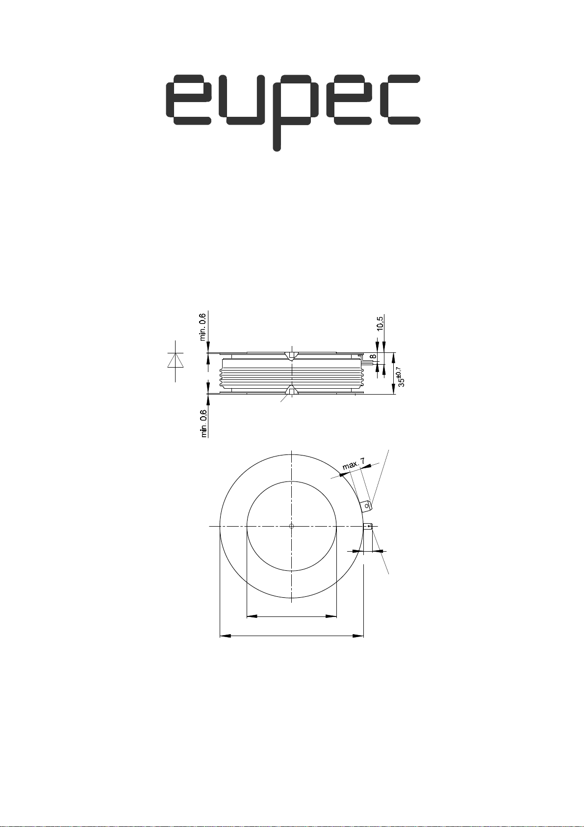
Maßbild, anliegend
outline, attached
) Gehäusegrenzstrom 40 kA (Sinushalbwelle 50 Hz)/Current limit of case 40 kA (sinusoidal half-wave 50 Hz)
tvj = -40°C...t
vj max
V
DRM
, V
RRM
V
Vorwärts-Stoßspitzensperrspannung non-repetitive peak forward off-state
Rückwärts-
non-repetitive peak reverse voltage tvj = +25°C...t
tvj = -40°C...t
vj max
vj max
Durchlaßstrom-Grenzeffektivwert RMS on-state current I
Dauergrenzstrom average on-state current tc = 85°C I
tc = 62°C 3400 A
Stoßstrom-Grenzwert surge current tvj = 25°C, tp = 10 ms I
Grenzlastintegral
I2 t-value
Kritische Stromsteilheit critical rate of rise of on-state current
tvj = t
tvj = 25°C, tp = 10 ms
tvj = t
vD ≤ 67%, v
, tp = 10 ms
vj max
, tp = 10 ms
vj max
, f = 50 Hz
DRM
iGM= 1,5 A, diG/dt = 1,5 A/µs
Kritische Spannungssteilheit critical rate of rise of off-state voltage tvj = t
Durchlaßspannung on-state voltage tvj = t
Schleusenspannung threshold voltage tvj = t
Ersatzwiderstand slope resistance tvj = t
, vD = 67% V
vj max
, iT = 10 kA v
vj max
vj max
vj max
DRM
Zündstrom gate trigger current tvj = 25 °C, vD = 6 V I
Zündspannung gate trigger voltage tvj = 25 °C, vD = 6 V V
Nicht zündender Steuerstrom gate non-trigger current tvj = t
tvj = t
Nicht zündende Steuerspannung gate non-trigger voltage tvj = t
Haltestrom holding current
Einraststrom latching current
tvj = 25 °C, vD = 12 V, RA = 4,7 Ω
tvj = 25 °C,vD = 12 V, RGK ≥ 10 Ω
, vD = 6 V I
vj max
, vD = 0,5 V
vj max
, vD = 0,5 V
vj max
DRM
DRM
iGM = 1 A, diG /dt = 1 A/µs, tg = 20 µs
Vorwärts- und Rückwärts-Sperrstrom forward off-state and reverse
tvj = t
vj max, vD
= V
DRM
, vR = V
RRM
V
= V
DSM
DRM
V
= V
RSM
RRM
TRMSM
TAVM
TSM
5300 A
2450 A
650001)
570001)
I2 t 21 . 106A2s
16 . 106A2s
(diT/dt)
(dv/dt)
T
V
T(TO)
r
T
GT
GT
GD
cr
cr
50 A/µs
1000 V/µs
max. 3,05 V
1,17 V
0,176
mΩ
max. 300 mA
max. 2,5 V
max. 20 mA
max. 10 mA
V
I
H
I
L
iD, i
GD
R
max. 0,4 V
max. 350 mA
max. 2000 mA
max. 430 mA
V
V
A
A
Zündverzug gate controlled delay time tvj=25°C, iGM = 1 A, diG/dt = 1 A/µs t
Freiwerdezeit circuit commutated turn-off time siehe Techn.Erl./see Techn. Inf. t
Innerer Wärmewiderstand für
thermal resistance, junction to case
Θ =180° el, sin
Übergangs-Wärmewiderstand thermal resistance, case to heatsink beidseitig/two-sided R
Höchstzul.Sperrschichttemperatur max. junction temperature t
Betriebstemperatur operating temperature t
Lagertemperatur storage temperature t
1
gd
q
R
vj max
c op
stg
thJC
thCK
max. 2,3 µs
typ. 370 µs
max. 0,0064 °C/W
max. 0,0015 °C/W
120 °C
-40...+120 °C
-40...+150 °C

T 2451 N
10
8
iT [kA]
6
4
2
0
0,5 1,0 1,5 2,0 2,5 3,53,0
T 2451 N / 1
Bild / Fig. 1
Grenzdurchlaßkennlinie / Limiting on-state characteristic
iT = f(vT), tvj = t
vj max
140
120
t
[°C]
C
100
80
vT [V]
10
180°
P
TAV
[W]
8
Θ= 30°
60°
Θ
0
120°
90°
6
4
2
0
T 2451 N / 2
1000 20000
3000
I
TAV
4000
[A]
Bild / Fig. 2
Durchlaßverlustleistung / On-state power loss P
Parameter : Stromflußwinkel / Current conduction angle θ
12
10
TAV
8
0 Θ
Θ= 30°
60°
90°
120°
Θ
0
P
[W]
180°
TAV
= f(I
TAV
)
DC
6
60
40
20
T 2451 N / 3
500 1000 1500 20000
2500 3000 3500
I
Bild / Fig. 3
Höchstzulässige Gehäusetemper atur / Max. allowable case temperature
tC = f(I
Beidseitige Kühlung / Two-sided cooling
TAVM
)
Parameter : Stromflußwinkel / Current conduction angle θ
Berechnungsgrundlage P
Calculation base P
TAV
(Schaltverluste gesonder t berücksichtigen) /
TAV
(switching losses should be c onsidered separately)
140
120
t
[°C]
C
100
80
60
40
TAVM
[A]
Θ= 180°
0 Θ
4
2
0
0
T 2451 N / 4
1000 2000
3000 4000 5000
Bild / Fig. 4
Durchlaßverlustleistung / On-state power loss P
Parameter : Stromflußwinkel / Current conduction angle θ
20
10
6
v
G
4
[V]
2
1
0,6
0,4
0,2
TAV
= f(I
TAV
I
TAV
)
6000
[A]
c
b
a
20
T 2451 N / 5
1000 20000
I
TAVM
3000500 1500 2500 3500
[A]
Bild / Fig. 5
Höchstzulässige Gehäusetemper atur / Max. allowable case temperature
tC = f(I
Beidseitige Kühlung / Two-sided cooling
TAVM
)
Parameter : Stromflußwinkel / Current conduction angle θ
Berechnungsgrundlage P
Calculation base P
TAV
(Schaltverluste gesonder t berücksichtigen) /
TAV
(switching losses should be c onsidered separately)
0,1
1
10
T 2451 N / 6
2 4 6
10
2
2 4 6
10
3
2 4 6
i
[mA]
G
Bild / Fig. 6
Steuercharakteristik mit Zündbereichen / Gate characteristic with trigging
areas vG = f(iG), VD = 6 V
Parameter : a b c
––––––––––––––––––––––––––––––––––––––––––––––––––––––––––
Steuerimpulsdauer / tr igger puls duration tg [ms] 10 1 0,5
––––––––––––––––––––––––––––––––––––––––––––––––––––––––––
Höchstzulässige Spitzensteuerverlustleistung /
Max. rated peak gate power dissipation [W] 20 40 60
––––––––––––––––––––––––––––––––––––––––––––––––––––––––––
4
10

2
10
6
4
t
2
gd
[µs]
1
10
6
4
2
0
10
6
4
2
-1
10
1
10
T 2451 N / 7
2 4 6
10
2
2 4 6
Bild / Fig. 7
Zündverzug / Gate controlled delay time tgd = f(iGM)
tvj = 25 °C, diG/dt = iGM/1µs
10
3
i
max
typ
2 4 6
[mA]
GM
T 2451 N
2
ITM= 2000 A
4
10
Q
r
[µAs]
7
5
4
3
2
4
10
0
10
T 2451 N / 8
2 3 4 5 7
Bild / Fig. 8
Sperrverzögerungsladung / Recovered c harge Qr = f(di/dt)
tvj = t
Parameter : Durchlaßstrom / On-state current i
vj max
, vR = 0,5 V
, vRM = 0,8 V
RRM
1
10
2 3 4 5 7
2
10
-di/dt [A/µs]
RRM
TM
0,008
0,007
Z
(th)JC
Θ
0
[°C/W]
0,005
0,004
0,003
0,002
0,001
0
-
3
10
T 2451 N / 9
10
Θ=
30°
60°
90°
120°
180°
-
2
-
1
10
0
10
Bild / Fig. 9
Transienter innerer Wärmewiderstand / Transient thermal impedance
Z
= f(t)
thJC
Parameter : Stromflußwinkel / c urrent conduction angle θ
0,008
0,007
0 Θ
Z
(th)JC
[°C/W]
0,005
0,004
10
Θ=
30°
60°
90°
120°
180°
DC
-
2
-
1
10
0
10
1
10
2
10
t [s]
0,003
0,002
0,001
0
-
1
10
2
10
t [s]
3
10
T 2451 N / 10
Bild / Fig. 10
Transienter innerer Wärmewiderstand / Transient thermal impedance
Z
= f(t)
thJC
Parameter : Stromflußwinkel / c urrent conduction angle θ
Analytische Elemente des transienten Wärmewiderstandes Z
Analytical elements of transient thermal impedance Z
R
τ
thn
[s]
n
Pos. n
[°C/W]
1 2 3 4 5
0,0003844 0,00074 0,00185 0,0038 0,00327
0,0012 0,007 0,056 0,27 3,08
thJC
pro Zweig für DC
thJC
per arm for DC
Analytische Funktion / Analytical function:
n
Z
thJC
max
= R
Σ
n=1
(1-e )
thn
t
-
τ
n
 Loading...