

European PowerSemiconductor and
Electronics Company
Marketing Information
T 1050 N T 1059 N
C
HK
G
A
ø3,5x3,5 deep
on both sides
ø50
ø50
max.12
+0,1
3,5
x 3,5 deep
on both sides
HK
plug A4,8x0,8
G
plug A2,8x0,8
74
ø 48
ø 48
C
A
HK
plug
4,8 x 0,8
4
G
plug
2,8 x 0,8
VWK June

T 1050 N T 1059 N
Elektrische Eigenschaften
Electrical properties
Höchstzulässige Werte
Maximum rated values
Periodische Vorwärts- und Rückwärts-
2000 2200 2400
2000 2200 2400
2100 2300 2500
Charakteristische Werte
Characteristic values
Thermische Eigenschaften
Thermal properties
Mechanische Eigenschaften
Mechanical properties
Spitzensperrspannung
repetitive peak forward off-state and
reverse voltages
tvj = -40°C...t
vj max
V
DRM
, V
RRM
2600 2800*
V
Vorwärts-Stoßspitzensperrspannung non-repetitive peak forward off-state
voltage
Rückwärts-Stoßspitzensperrspannung non-repetitive peak reverse voltage tvj = +25°C...t
tvj = -40°C...t
vj max
vj max
Durchlaßstrom-Grenzeffektivwert RMS on-state current I
Dauergrenzstrom average on-state current tc = 85°C I
tc = 64°C 1400 A
Stoßstrom-Grenzwert surge current tvj = 25°C, tp = 10 ms I
tvj = t
, tp = 10 ms 19000 A
vj max
Grenzlastintegral
I2 t-value
Kritische Stromsteilheit critical rate of rise of on-state current
tvj = 25°C, tp = 10 ms
tvj = t
, tp = 10 ms
vj max
vD ≤ 67%, v
, f = 50 Hz
DRM
iGM= 1 A, diG/dt = 1 A/µs
Kritische Spannungssteilheit critical rate of rise of off-state voltage tvj = t
, vD = 67% V
vj max
DRM
5.Kennbuchstabe/5th letter C (dv/dt)
5.Kennbuchstabe/5th letter F (dv/dt)
Durchlaßspannung on-state voltage tvj = t
Schleusenspannung threshold voltage tvj = t
Ersatzwiderstand slope resistance tvj = t
, iT = 4200 A v
vj max
vj max
vj max
Zündstrom gate trigger current tvj = 25 °C, vD = 6 V I
Zündspannung gate trigger voltage tvj = 25 °C, vD = 6 V V
Nicht zündender Steuerstrom gate non-trigger current tvj = t
Nicht zündende Steuerspannung gate non-trigger voltage tvj = t
Haltestrom holding current
Einraststrom latching current
, vD = 6 V I
vj max
, vD = 0,5 V
vj max
DRM
tvj = 25 °C, vD = 6 V, RA = 5 Ω
tvj = 25 °C,vD = 6 V, RGK ≥ 10 Ω
iGM = 1 A, diG /dt = 1 A/µs, tg = 20 µs
Vorwärts- und Rückwärts-Sperrstrom forward off-state and reverse currents tvj = t
vj max, vD
= V
DRM
, vR = V
RRM
Zündverzug gate controlled delay time tvj=25°C, iGM = 1 A, diG/dt = 1 A/µs t
Freiwerdezeit circuit commutated turn-off time siehe Techn.Erl./see Techn. Inf. t
V
= V
DSM
V
RSM
TRMSM
TAVM
TSM
= V
DRM
RRM
2600 2800*
2700 2900
2200 A
1050 A
21000 A
I2 t 2,205 . 106A2s
1,805 . 106A2s
(diT/dt)
cr
150 A/µs
500 V/µs
1000 V/µs
max. 2,48 V
1,05 V
0,3
mΩ
max. 250 mA
max. 2 V
max. 100 mA
max. 0,25 V
max. 500 mA
max. 2,5 A
max. 200 mA
max. 4,5 µs
typ. 300 µs
V
r
T
GT
GD
V
I
H
I
L
iD, i
gd
q
cr
cr
T
T(TO)
GT
GD
R
V
V
Innerer Wärmewiderstand für beidseitige
thermal resistance, junction to case for
Θ =180° el, sin
R
thJC
max. 0,021 °C/W
DC max. 0,02 °C/W
für anodenseitige Kühlung for anode-sided cooling
Θ =180° el, sin
R
thJC(A)
max. 0,036 °C/W
DC max. 0,035 °C/W
für kathodenseitige Kühlung for cathode-sided cooling
Θ =180° el, sin
R
thJC(K)
max. 0,048 °C/W
DC max. 0,047 °C/W
Übergangs-Wärmewiderstand thermal resistance, case to heatsink beidseitig/two-sided R
thCK
max. 0,004 °C/W
einseitig/one-sided max. 0,008 °C/W
Höchstzul.Sperrschichttemperatur max. junction temperature t
Betriebstemperatur operating temperature t
Lagertemperatur storage temperature t
vj max
c op
stg
125 °C
-40...+125 °C
-40...+150 °C
Si-Elemente mit Druckkontakt Si-pellet with pressure contact
Anpreßkraft clamping force F 20...45 kN
Gewicht weight T 1050 N/T 1059 N G typ. 600/540 g
Kriechstrecke creepage distance T 1050 N/T 1059 N 323/25 mm
Feuchteklasse humidity classification DIN 40040 C
Schwingfestigkeit vibration resistance f = 50 Hz 50 m/s²
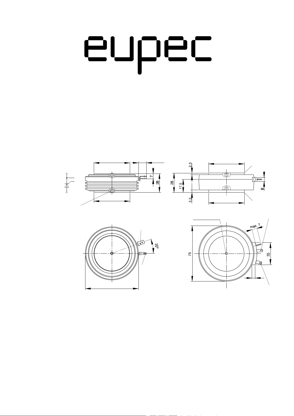
Maßbild, anliegend outline, attached DIN 41814-155B4
* Für größere Stückzahlen Liefertermin erfragen / Delivery for larger quantities on request

T 1050 N, T 1059 N
5
i
T
[kA]
4
tvj = 25 °C
3
a
2
b
1
0
T 1050 N / 1 v
1,51 2 2,5 3
Bild / Fig. 1
Durchlaßkennlin ie / On-state c haracteristic iT = f(vT), tvj = t
a -Typis che Kennlin ien / typical characteristic s
b -Grenzkennl inien / limiting c haracteristics
120
t
100
C
[°C]
3
90 °
tvj = 125 °C
P
TAV
[kW]
2,5
0 Θ
2
Θ = 30 °
60 °
1,5
1
0,5
0
[V]
T
0,2 0,4 0,6 0,8 1 1,2 1,4 1,6
Bild / Fig. 2
vj max
Durchlaßverlustle istung / O n-state power loss P
Parameter: Stromflußwink el / Current conduction angle θ
TAV
120
0 Θ 0 Θ
t
100
A
[°C]
= f(I
120 °
I
TAV
TAV
180 °
[kA]T 1050 N / 2
)
80
60
40
20
0,2 0,4 0,6 0,8 1 1,2 1,4 1,6
60 ° 90 ° 120 ° 180 °Θ = 30 °
I
TAVM
Bild / Fig. 3
Höchstzuläs sige Gehä use tempe ratur / Max. allowable c ase temperature
tA = f(I
)
TAVM
Anodenseitige Kühlung / Anode-sided coolin g
Bei dseitig e Kühlun g / Two-sided co oli ng
Parameter: Stromflu ßwink el / Current conduction angle θ
120
t
100
C
[°C]
80
60
[kA]T 1050 N / 3
0 Θ
80
60
60 °
90 °
120 °
180 °
30 ° 60 ° 90 ° 120 ° 180 °
I
TAVM
40
20
Θ = 30 °
100 200 300 400 600500 700 800
Bild / Fig. 4
Höchstz ulässi ge Kühlmitte ltempe ratur / Max. allowable cooling medi um
temperature tA = f(I
Kühlkörper / Heatsink: K0.05F
TAVM
)
Luftseb stkü hlung / Natural air-coo ling, tA = 45 °C
Verstärkte Luftkühlun g / Forced ai r-cooling, tA = 35°C, VL = 120 l/s
Parameter: Stromflußwink el / Current conduction angle θ
4
P
TAV
[kW]
0 Θ
Θ = 3 0 °
60 °
90 °
180 °
120 °
2
[A]T 1050 N / 4
DC
40
20
Θ = 30 °
0,4 0 ,8 1,2 1,6 2 2,4
T 1050 N / 5
60 ° 90 ° 120 ° 180 °
Bild / Fig. 5
Durchlaßverlustl eistun g / On-state power los s P
Parameter: Stromflu ßwink el / Current conduction angle θ
TAV
= f(I
I
TAVM
TAV
DC
[A]
0
T 1050 N / 6
0,4 0,8 1,2 1 ,6 2 2,4
I
[kA]
TAV
Bild / Fig. 6
)
Höchstz ulässi ge Gehäusetemperatur / Max. all owable case temperature
tA = f(I
)
TAVM
Anodenseitige Kühlu ng / Anode-sided cooling
Beid sei tige Kühlung / Two-sided coo li ng
Parameter: Stromflußwink el / Current conduction angle θ

current I
120
t
100
A
[°C]
80
60
90 °
120 °
40
20
90 °
120 °
30 ° 60 °
180 °
DC
60 °
Θ = 30 °
200 400 600 800 1000
Bild / Fig. 7
Höchstzuläs sige Kühlmitteltemperatur / Max. allowable coolin g med ium
temperature tA = f(I
Kühlkö rper / Heatsi nk: K0. 05F
TAVM
)
Luftsebstkühlun g / Natural air-cooling, tA = 45°C
Verstärkte Luftkühlu ng / Forced air-cooli ng, tA = 35°C, VL = 120 l/s
Parameter: Stromflu ßwink el / Current conduction angle θ
I
TAVM
180 °
[A]T 1050 N / 7
0 Θ
DC
4
3
I
= 0 A
TAV(vor)
2
50 A
100 A
150 A
200 A
100 1 10 1 10 1h10
ms s min
I
T(OV)
[kA]
1
10
8
5
4
3
2
0
10
8
5
4
2 3 5 2 3 5 2 3 5 2 3 2 3 5 2 3
T 105 0 N / 8
Bild / Fig. 8
Überstrom / Overload on-state current I
Luftselbstk ühlung / Natural air-cooli ng, tA = 45°C
Kühlkörper / Heatsink: K0.05F
Parameter: Vorlaststrom / Pre-load current I
T 1050 N, T 1059 N
t
= f(t)
T(OV)
TAV(vor)
4
3
2
I
T(OV)
[kA]
1
10
8
450 A
5
600 A
4
3
2
0
10
2 3 5 2 3 5 2 3 5 2 3 2 3 5 2 3
T 1050 N / 9
I
=
TAV(vor)
0 A
150 A
300 A
100 1 10 1 10 1h1 0
ms s m in
Bild / Fig. 9
Überstrom / Overload on-state current I
Verstärkte Luftkühlu ng / Forced air-cooli ng, tA= 35 °C
T(OV)
= f(t)
Kühlkö rper / Heatsi nk: K0. 05F, VL = 120 l/s
Parameter: Vorlaststrom / Pre-load current I
5
20s
4s
I
TIN T
[kA]
I
TAV(vor)
= 0
4
1min
3
4min
10min
2
40min
1
2h
0
2
0,1
T 1050 N / 11
1s
0,4s
2 5
5 2
1
DR [%
10
]
SD =
0,1s
10051
TAV(vor)
I
TAV(vor)
= 600 A
I
TAV(vor)
2 3 4
Bild / Fig. 11
Höchstzuläs siger Durchlaßstrom bei Aus setzbetrieb / Max. al lowable
on-stat e current at intermittent operation I
Verstärkte Luftkühlu ng / Forced air-cooli ng, tA = 35°C
TI NT
= f(ED)
Kühlkö rper / Heatsi nk: K0. 05F, VL = 120 l/s
Parameter: Spi eldauer / Cycle durati on SD
Vorlaststrom / Pre-load cu rrent I
TAV(vor)
I
TIN T
450 A
SD
t
[A
300 A
]
150 A
0 A
I
TINT
5
I
= 200 A
TAV(vor)
I
TAV(vor)
1
SD
2 3 4
I
TIN T
I
TIN T
[kA]
I
TAV(vor)
= 0
20s
4
1min
3
4min
2
10m in
40m in
1
2h
0
2
0,1
T 1050 N / 10
4s
1s
0,4s
2 5
5 2
1
10
DR [%
SD =
0,1s
5
100
]
Bild / Fig. 10
Höchstz ulässi ger Durch laßstrom bei Aus setzbetrieb / Max. allo wable
on-state current at intermittent operation I
Luftselbstk ühlung / Natural air-cooli ng, tA = 45°C
TIN T
= f(ED)
Kühlkörper / Heatsink: K0.05F
Parameter: Spie ldauer / Cycl e duration SD
Vorlaststrom / Pre-load current I
TAV(vo r)
20
a
I
T(0V)M
[kA]
10
0
1
10
T 1050 N / 12
b
K 0,05F ; tA = 35°C
K 0, 05F; tA = 45°C
2 3 4 5 7 2 3 4 5 7 2 3 4 5 7
10
2
10
3
t [ms]
Bild / Fig. 12
Grenzs trom / Max. overl oad on-state current I
Luftselbstk ühlung / Natural air-cooli ng, tA = 45°C
= f(t), vRM = 0,8 V
T(OV)M
Verstärkte Luftkühlu ng / Forced air-cooli ng, tA = 35°C, VL = 120 l/ s
Kühlkörper / Heatsink: K0.05F
Bela stung aus / Surge current occ urs:
a - Leerlauf / No-load co ndit ions
b - Betrieb mit Dauergrenzstrom / During operation at max. averag e on-state
150 A
[A
100 A
50 A
I
TINT
]
VL = 120 l/ s
RRM
0 A
4
10

1
10
8
6
4
v
3
G
[V]
2
0
10
8
6
4
3
2
-1
10
1
10
T 1050 N / 13 i
2
10
3
10
Bild / Fig. 13
Steuercharakteristik mit Zündbereichen / Gate chara cteris tic with trigging
areas vG = f(iG), VD = 6 V
Parameter: a b c
––––––––––––– –––––––––––––––––––––––––––––– –––––––––––––––
Steuerimpuls dauer / trigge r puls duration tg [ms] 10 1 0,5
––––––––––––– –––––––––––––––––––––––––––––– –––––––––––––––
Höchstzuläs sige Spit z ensteuerverlustl eistung /
Max . rated peak gate power dissipa tion [W] 20 40 60
––––––––––––– –––––––––––––––––––––––––––––– –––––––––––––––
4
10
8
7
6
Q
r
5
[µAs ]
4
3
2
3
10
0
10
T 1050 N / 15
2 3 4 5 6 8 2 3 4 5 6 8
10
1
-di/dt [A/µs ]
Bild / Fig. 15
Sperrverzögerungsladung / Recovered charg e Qr = f(di/dt)
tvj = t
Parameter: Durchlaßstrom / On-state current i
vj max
, vR = 0,5 V
, vRM = 0,8 V
RRM
RRM
TM
G
[mA]
T 1050 N, T 1059 N
3
10
c
b
a
42 3 4 5 6 8 2 3 4 5 6 8 2 3 4 5 6 8
10
i
=
2000 A
TM
1000 A
500 A
200 A
100 A
50 A
20 A
2
10
5
2
2
10
t
gd
[µs]
5
2
1
10
5
2
0
10
5
2
-1
10
1
2 3 4 5 6 8 2 3 4 5 6 8 2 3 4 5 6 8
10
T 1050 N / 14 i
2
10
a
b
3
10
[mA]
G
Bild / Fig. 14
Zündverzug / Gate controlled dela y time tgd = f(iG)
tvj = 25 °C, diG/dt = iGM/1µs
a - Maximale r Verlauf / Limiting c haracteristic
b - Typischer Verla uf / Typic al characteristic
0,044
0 Θ
0,036
Z
t hJC
[°C/W]
0,028
0,020
f = 50 Hz
0,012
Θ = 30 °
60 °
90 °
120 ° 180 °
0,004
2 5 2 5 2 5 2 4 2 5
0,01 0,1 1 10 1 10
T 1050 N / 16
s min
t
Bi ld / Fig. 16
Transienter innerer Wärmewiderstand / Transient thermal imped ance
Z
= f(t)
thJ C
Anodenseitige Kühlung / Anode-sided cooli ng
Beids eitige Kühlu ng / Two-si ded c ooling
Parameter: Stromf lußwin kel / current conduct ion angle θ
10
4
0,05
0 Θ
Z
t hJC
[°C/W]
0,03
0,02
f = 50 Hz
0,01
0
10
Θ = 30 °
60 °
90 °
120 °
180 °
DC
2 5 2 5 2 5 2 5 2
-3
T 1050 N / 17
-2
10
-1
10
0
10
10
Bild / Fig. 17
Transienter inne rer Wärmewiderstand / Transient thermal impedance
Z
= f(t)
thJ C
Anodenseitige Kühlung / Anode-side d coo ling
Beids eitige Kühlu ng / Two-si ded c ooling
Parameter: Stromf lußwi nkel / current condu ction ang le θ
1
1min 2 mi n
t [s ]
Analy tische Ele mente des transienten Wärmewiderstandes Z
Analy tical el ements of transient thermal impedance Z
per arm for DC
t hJC
Beids eitig / Two-sided
R
τ
thn
[s]
n
Pos. n
[°C/W]
1 2 3 4 5 6
0,00094 5 0,00203 5 0,0043 5 0,0084 0,00427
0,00173 0,014 0,114 0,94 5, 1
Anodenseiti g / Anode -sided
R
τ
thn
[s]
n
Pos. n
[°C/W]
1 2 3 4 5 6
0,00194 0,0037 0,00736 0,0109 0,0111
0,0032 0,058 0,55 4,2 36,3
Kathoden se itig / Cathode-sided
R
τ
thn
[s]
n
Pos. n
[°C/W]
1 2 3 4 5 6
0,00124 0,0032 0,00576 0,01 0,012 0,014 8
0,0021 0,028 0,0336 2 10 52 ,5
Analy tische Funktion / Analytical function:
n
Z
t hJC
max
= R
Σ
n=1
(1-e )
thn
t
-
τ
n
pro Zweig für DC
thJ C
 Loading...