

现货库存、技术资料、百科信息、热点资讯,精彩尽在鼎好!
j
)
j
A
j
g
Preliminary data
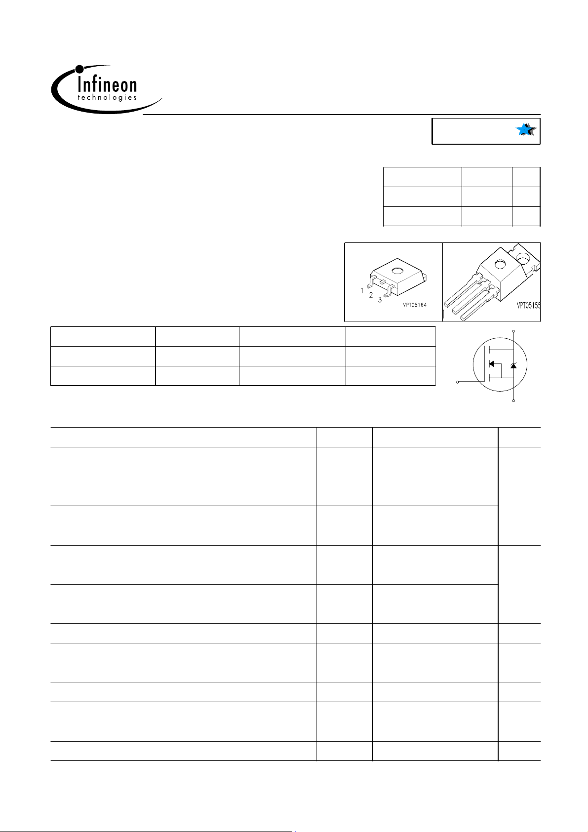
SPP20N60S5
SPB20N60S5
Cool MOS™====Power Transistor
•=New revolutionary high voltage technology
• Worldwide best R
• Ultra low gate charge
•=Improved periodic avalanche rating
• Extreme dv/dt rated
•=Optimized capacitances
•=Improved noise immunity
•=Former development designation:
SPPx1N60S5/SPBx1N60S5
Type Package Ordering Code
SPP20N60S5
SPB20N60S5 P-TO263-3-2 Q67040-S4171
in TO 220
DS(on)
P-TO220-3-1 Q67040-S4751
OO
L
MOS
C
Power Semicon d uctors
Product Summary
VDS @ T
R
DS(on
I
D
P-TO263-3-2 P-TO220-3-1
max
650 V
0.19 Ω
20 A
Marking
20N60S5
20N60S5
G,1
D,2
S,3
Maximum Ratings,at Tj = 25 °C, unless otherwise specified
Parameter Symbol Value Unit
Continuous drain current
TC=25°C
T
=100°C
C
Pulsed drain current
TC=25°C
1)
Avalanche energy, single pulse
I
= 10 A, VDD = 50 V
D
Avalanche energy (repetitive, limited by T
jmax
I
D
20
13
I
D puls
E
AS
)
E
AR
40
690 mJ
1
A
ID = 20 A, VDD = 50 V
Avalanche current (repetitive, limited by T
Reverse diode dv/dt
IS=20A, VDS<V
, di/dt=100A/µs, T
DSS
jmax
=150°C
max
) I
dv/dt
Gate source voltage V
Power dissipation
TC=25°C
P
R
GS
tot
20 A
6 kV/µs
±20
V
208 W
Operating and storage temperature T
1
T
,
st
-55... +150
°C
2001-07-25
SPP20N60S5
Preliminary data
Electrical Characteristics, at Tj = 25 °C, unless otherwise specified
Parameter Symbol Values Unit
min. typ. max.
Thermal Characteristics
SPB20N60S5
Thermal resistance, junction - case R
Thermal resistance, junction - ambient
R
thJC
thJA
(Leaded and through-hole packages)
SMD version, device on PCB:
R
thJA
@ min. footprint
@ 6 cm2 cooling area
2)
Static Characteristics, at Tj = 25 °C, unless otherwise specified
Drain-source breakdown voltage
V
(BR)DSS
600 - - V
VGS = 0 V, ID = 0.25 mA
Gate threshold voltage, VGS = VDS
V
GS(th)
3.5 4.5 5.5
ID = 1 mA, Tj = 25 °C
Zero gate voltage drain current, VDS=V
DSS
I
DSS
VGS = 0 V, Tj = 25 °C
VGS = 0 V, Tj = 150 °C
- - 0.6 K/W
-
-
-
-
-
-
-
35
0.5
-
62
62
-
25
250
µA
Gate-source leakage current
VGS = 20 V, VDS = 0 V
Drain-source on-state resistance
VGS = 10 V, ID = 13 A
1
current limited by T
2
Device on 40mm*40mm*1.5mm epoxy PCB FR4 with 6 cm
connection. PCB is vertical without blown air.
jmax
I
GSS
R
DS(on)
- - 100 nA
- 0.16 0.19
Ω
² (one layer, 70µm thick) copper area for drain
2
2001-07-25
SPP20N60S5
)
)
f
g
g
Preliminary data
Electrical Characteristics, at Tj = 25 °C, unless otherwise specified
Parameter Symbol Conditions Values Unit
min. typ. max.
Dynamic Characteristics
SPB20N60S5
Transconductance g
Input capacitance C
Output capacitance C
Reverse transfer capacitance C
Turn-on delay time t
Rise time t
Turn-off delay time t
Fall time t
Gate Charge Characteristics
Gate to source charge Q
Gate to drain charge Q
Total gate charge Q
fs
iss
oss
rss
d(on
r
d(off
s
d
g
VDS≥2*ID*R
I
=13A
D
VGS=0V, VDS=25V,
f=1MHz
DS(on)max
,
- 12 - S
- 3000 - pF
- 1170 -
- 28 -
VDD=350V, VGS=10V,
I
=20A, RG=5.7Ω
D
- 120 - ns
- 25 -
- 140 210
- 30 45
VDD=350V, ID=20A - 21 - nC
- 47 -
VDD=350V, ID=20A,
V
=0 to 10V
GS
- 79 103
Reverse Diode
Inverse diode continuous
I
forward current
Inverse diode direct
I
current,pulsed
Inverse diode forward voltage V
Reverse recovery time t
Reverse recovery charge Q
S
SM
SD
rr
rr
TC=25°C - - 20 A
- - 40
VGS=0V, IF=20A - 1 1.2 V
VR=100V, I
di
/dt=100A/µs
F
lS,
=
F
- 610 - ns
- 12 - µC
3
2001-07-25

Preliminary data
SPP20N60S5
SPB20N60S5
Power dissipation
P
= f (TC)
tot
SPP20N60S5
240
W
200
180
160
tot
P
140
120
100
80
60
40
20
0
0 20 40 60 80 100 120
°C
Drain current
ID = f (TC)
parameter: VGS≥ 10 V
SPP20N60S5
22
A
18
16
14
D
I
12
10
8
6
4
2
160
T
C
0
0 20 40 60 80 100 120
°C
160
T
C
Safe operating area
ID=f (VDS)
parameter: D=0.01, TC=25°C
2
SPP20N60S5
10
A
1
10
D
I
0
10
-1
10
10
D
R
0
D
I
/
S
D
V
=
)
n
o
(
S
1
10
10
Transient thermal impedance
Z
= f (tp)
thJC
parameter : D = tp/T
SPP20N60S5
1
10
K/W
tp = 11.0µs
0
10
-1
10
thJC
100 µs
1 ms
10 ms
DC
2
V
V
DS
10
3
Z
-2
10
10
10
10
-3
-4
-5
10
single pulse
-7
10
-6
-5
10
-4
10
10
D = 0.50
0.20
0.10
0.05
0.02
0.01
-3
10
-2
s
t
0
10
p
4
2001-07-25

Preliminary data
SPP20N60S5
SPB20N60S5
Typ. output characteristic
ID = f (VDS)
Parameter: VGS, Tj = 25 °C
75
A
60
55
50
D
I
45
40
35
30
25
20
15
10
5
0
0 5 10 15 20
20V
15V
12V
11V
10V
9V
8V
7V
V
V
DS
30
Drain-source on-resistance
R
DS(on)
= f (Tj)
parameter : ID = 13 A, VGS = 10 V
SPP20N60S5
1.1
Ω
0.9
0.8
DS(on)
0.7
R
0.6
0.5
0.4
0.3
0.2
0.1
0
-60 -20 20 60 100
98%
typ
°C
180
T
j
Typ. transfer characteristics
ID= f ( VGS )
VDS≥ 2 x ID x R
70
A
60
55
50
45
D
I
40
35
30
25
20
15
10
5
0
0 2 4 6 8 10 12 14 16
DS(on)max
V
V
GS
20
Typ. capacitances
C = f (VDS)
parameter: VGS=0 V, f=1 MHz
5
10
4
10
C
iss
3
10
pF
C
oss
2
10
C
1
10
0
10
0 10 20 30 40 50 60 70 80
rss
V
V
100
DS
5
2001-07-25

Preliminary data
SPP20N60S5
SPB20N60S5
Avalanche Energy
EAS = f (Tj)
par.: ID = 10 A, VDD = 50 V
750
mJ
600
550
500
AS
E
450
400
350
300
250
200
150
100
50
0
20 40 60 80 100 120
°C
Avalanche SOA
IAR = f (tAR)
par.: Tj ≤ 150 °C
20
A
AR
I
10
(START)
T
5
(START)
T
0
-3
160
T
j
10
10
-2
=125°C
j
-1
10
10 0 10 1 10
=25°C
j
2
µs
t
AR
10
4
Drain-source breakdown voltage
V
(BR)DSS
(BR)DSS
V
= f (Tj)
SPP20N60S5
720
V
680
660
640
620
600
580
560
540
-60 -20 20 60 100
°C
Gate threshold voltage
V
GS(th)
= f (Tj)
parameter: VGS = VDS, ID = 1 mA
7
V
5
GS(th)
V
4
3
2
1
180
T
j
0
-60 -20 20 60 100
°C
max.
typ.
min.
T
180
j
6
2001-07-25

Preliminary data
SPP20N60S5
SPB20N60S5
Forward characteristics of reverse diode
IF = f (VSD)
parameter: Tj , tp = 10 µs
2
SPP20N60S5
10
A
1
10
F
I
0
10
Tj = 25 °C typ
Tj = 150 °C typ
Tj = 25 °C (98%)
Tj = 150 °C (98%)
-1
10
0 0.4 0.8 1.2 1.6 2 2.4
V
3
V
SD
Typ. gate charge
V
= f (Q
GS
parameter: I
SPP20N60S5
16
V
12
GS
10
V
8
6
4
2
0
0 20 40 60 80
Gate
Dpuls
)
= 20 A
0,2
V
DS max
0,8 V
nC
DS max
Q
g
120
7
2001-07-25

Preliminary data
SPP20N60S5
SPB20N60S5
P-TO220-3-1
P-TO220-3-1
dimensions
symbol
A 9.70 10.30 0.3819 0.4055
B 14.88 15.95 0.5858 0.6280
C 0.65 0.86 0.0256 0.0339
D 3.55 3.89 0.1398 0.1531
E 2.60 3.00 0.1024 0.1181
F 6.00 6.80 0.2362 0.2677
G 13.00 14.00 0.5118 0.5512
H 4.35 4.75 0.1713 0.1870
K 0.38 0.65 0.0150 0.0256
L 0.95 1.32 0.0374 0.0520
M
N 4.30 4.50 0.1693 0.1772
P 1.17 1.40 0.0461 0.0551
T 2.30 2.72 0.0906 0.1071
[mm] [inch]
minmaxminmax
2.54 typ. 0.1 typ.
TO-26 3 (D ²Pak/P- T O 220SMD)
dimensions
symbol [mm] [inch]
min max min max
A 9.80 10.20 0.3858 0.4016
B 0.70 1.30 0.0276 0.0512
C 1.00 1.60 0.0394 0.0630
D 1.03 1.07 0.0406 0.0421
E
F 0.65 0.85 0.0256 0.0335
G
H 4.30 4.50 0.1693 0.1772
K 1.17 1.37 0.0461 0.0539
L 9.05 9.45 0.3563 0.3720
M 2.30 2.50 0.0906 0.0984
N
P 0.00 0.20 0.0000 0.0079
Q 4.20 5.20 0.1654 0.2047
R
S 2.40 3.00 0.0945 0.1181
T 0.40 0.60 0.0157 0.0236
U
V
W
X
Y
Z
2.54 typ.
5.08 typ.
15 typ.
8° max
10.80
1.15
6.23
4.60
9.40
16.15
0.1 typ.
0.2 typ.
0.5906 typ.
8° max
0.4252
0.0453
0.2453
0.1811
0.3701
0.6358
8
2001-07-25

SPP20N60S5
Preliminary data
Published by
Infineon Technologies AG,
Bereichs Kommunikation
St.-Martin-Strasse 53,
D-81541 München
© Infineon Technologies AG 1999
All Rights Reserved.
Attention please!
The information herein is given to describe certain components and shall not be considered as warranted
characteristics.
Terms of delivery and rights to technical change reserved.
We hereby disclaim any and all warranties, including but not limited to warranties of non-infringement,
regarding circuits, descriptions and charts stated herein.
Infineon Technologies is an approved CECC manufacturer.
Information
For further information on technology, delivery terms and conditions and prices please contact your nearest
Infineon Technologies Office in Germany or our Infineon Technologies Reprensatives worldwide (see address list).
Warnings
Due to technical requirements components may contain dangerous substances.
For information on the types in question please contact your nearest Infineon Technologies Office.
Infineon Technologies Components may only be used in life-support devices or systems with the express
written approval of Infineon Technologies, if a failure of such components can reasonably be expected to
cause the failure of that life-support device or system, or to affect the safety or effectiveness of that device
or system Life support devices or systems are intended to be implanted in the human body, or to support
and/or maintain and sustain and/or protect human life. If they fail, it is reasonable to assume that the health
of the user or other persons may be endangered.
SPB20N60S5
9
2001-07-25
 Loading...