

SPD06N80C3
)
)
j
A
j
A
j
g
Cool MOS™ Power Transistor
Feature
• New revolutionary high voltage technology
• Worldwide best R
DS(on
• Ultra low gate charge
• Periodic avalanche rated
• Extreme dv/dt rated
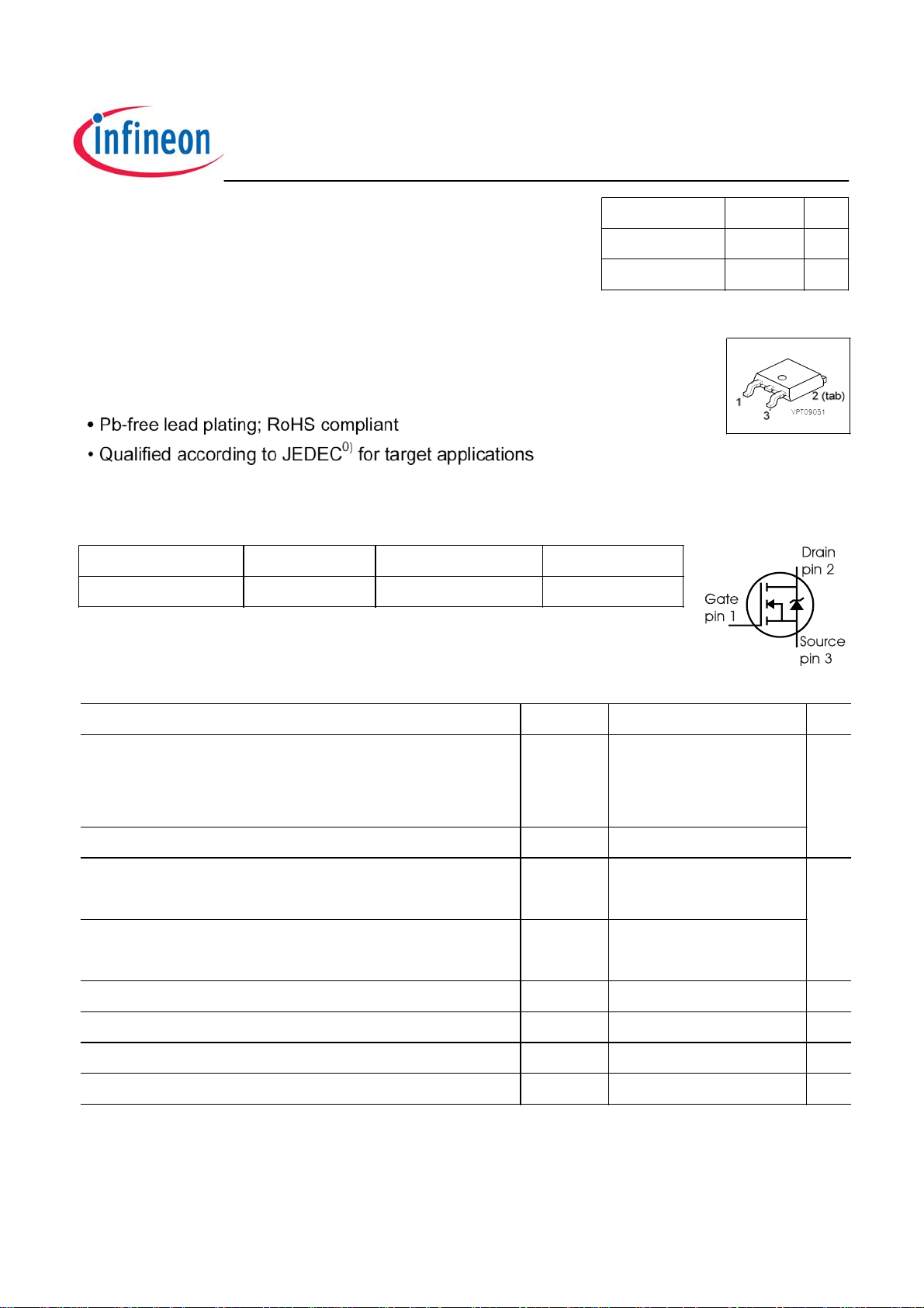
Type Package Ordering Code
SPD06N80C3 PG-TO252 Q67040-S4352
in TO252
Marking
06N80C3
V
R
DS(on
DS
I
800 V
0.9 Ω
D
6 A
PG-TO252
Maximum Ratings, at T
Parameter
Continuous drain current
T
= 25 °C
C
T
= 100 °C
C
Pulsed drain current, tp limited by T
Avalanche energy, single pulse
I
=1.2A, V
D
DD
=50V
Avalanche energy, repetitive t
I
=6A, V
D
DD
=50V
Avalanche current, repetitive t
= 25°C, unless otherwise specified
C
Symbol Value Unit
I
max
I
E
1)
limited by T
AR
limited by T
R
jmax
max
E
I
Gate source voltage V
Power dissipation, T
= 25°C
C
P
Operating and storage temperature T
D
Dpuls
AS
AR
R
GS
tot
, T
A
6
3.8
18
230 mJ
0.2
6 A
±20
V
83 W
st
-55... +150
°C
Rev. 2.4 Page 1
2008-04-11

Maximum Ratings
)
SPD06N80C3
Parameter
Drain Source voltage slope
V
= 640 V, I
DS
= 6 A, T
D
= 125 °C
j
Symbol Value Unit
dv/dt 50 V/ns
Thermal Characteristics
Parameter Symbol Values Unit
min. typ. max.
Thermal resistance, junction - case
Thermal resistance, junction - ambient, leaded
SMD version, device on PCB:
@ min. footprint
@ 6 cm
2
cooling area
2)
Soldering temperature, reflow soldering, MSL3
1.6 mm (0.063 in.) from case for 10s
3)
R
R
R
T
thJC
thJA
thJA
sold
- - 1.5 K/W
- - 62
-
-
-
-
75
50
- - 260 °C
Electrical Characteristics
Parameter
Symbol Conditions Values Unit
Drain-source breakdown voltage
Drain-Source avalanche
V
V
breakdown voltage
Gate threshold voltage V
Zero gate voltage drain current I
Gate-source leakage current I
Drain-source on-state resistance R
Gate input resistance
R
(BR)DSS
(BR)DS
GS(th
DSS
GSS
DS(on)
G
min. typ. max.
V
=0V, ID=0.25mA 800 - - V
GS
V
=0V, ID=6A - 870 -
GS
I
=250µΑ, VGS=V
D
VDS=800V, V
T
=25°C,
j
T
=150°C
j
VGS=20V, V
V
=10V, ID=3.8A,
GS
T
=25°C
j
T
=150°C
j
f=1MHz, open Drain - 0.7 -
=0V,
GS
=0V - - 100 nA
DS
2.1 3 3.9
DS
-
-
-
-
0.5
-
0.78
2.1
10
100
0.9
µA
Ω
-
Rev. 2.4 Page 2
2008-04-11
SPD06N80C3
j
(
)
Electrical Characteristics , at T
Parameter
Symbol Conditions Values Unit
Transconductance g
Input capacitance C
Output capacitance C
Reverse transfer capacitance C
Effective output capacitance,
4)
C
energy related
Effective output capacitance,
5)
C
time related
Turn-on delay time t
Rise time t
Turn-off delay time t
Fall time t
= 25 °C, unless otherwise specified
min. typ. max.
V
fs
iss
oss
rss
o(er)
o(tr)
d(on)
r
d(off)
f
≥2*ID*R
DS
I
=3.8A
D
VGS=0V, V
f=1MHz
V
=0V,
GS
V
=0V to 480V
DS
VDD=400V, V
I
=6A, R
D
T
=125°C
j
DS
=15Ω,
G
DS(on)max
=25V,
GS
,
=0/10V,
- 4 - S
- 785 - pF
- 390 -
- 20 -
- 22 - pF
- 42 -
- 25 - ns
- 15 -
- 65 75
- 8 11
Gate Charge Characteristics
Gate to source charge
Gate to drain charge Q
Gate charge total Q
Gate plateau voltage V
1
Repetitve avalanche causes additional power losses that can be calculated as P
2
Device on 40mm*40mm*1.5mm epoxy PCB FR4 with 6cm² (one layer, 70 µm thick) copper area for drain
connection. PCB is vertical without blown air.
3
Soldering temperature for TO-263: 220°C, reflow
4
C
is a fixed capacitance that gives the same stored energy as C
o(er)
5
C
is a fixed capacitance that gives the same charging time as C
o(tr)
Q
gs
gd
g
plateau
V
=640V, ID=6A - 3.3 - nC
DD
- 14 -
V
=640V, ID=6A,
DD
V
=0 to 10V
GS
V
=640V, ID=6A - 6 - V
DD
while V
oss
while V
oss
- 27 35
=EAR*f.
AV
is rising from 0 to 80% V
DS
is rising from 0 to 80% V
DS
DSS
DSS
.
.
Rev. 2.4 Page 3
2008-04-11
SPD06N80C3
j
Electrical Characteristics, at T
Parameter
Inverse diode continuous
= 25 °C, unless otherwise specified
Symbol Conditions Values Unit
I
S
forward current
Inverse diode direct current,
I
SM
pulsed
Inverse diode forward voltage V
Reverse recovery time t
Reverse recovery charge Q
Peak reverse recovery current I
Peak rate of fall of reverse
SD
rr
rr
rrm
dirr/dt
recovery current
Typical Transient Thermal Characteristics
min. typ. max.
T
=25°C - - 6 A
C
- - 18
V
=0V, IF=I
GS
V
=400V, IF=IS ,
R
di
/dt=100A/µs
F
S
- 1 1.2 V
- 520 - ns
- 5 - µC
- 18 - A
- 400 - A/µs
Symbol Value Unit Symbol Value Unit
typ. typ.
Thermal resistance
R
th1
R
th2
R
th3
R
th4
R
th5
R
th6
P
tot
0.024 K/W
0.024
0.086
0.309
0.317
0.112
T
R
j T
th1
(t)
C
th1
C
th2
Thermal capacitance
C
th1
C
th2
C
th3
C
th4
C
th5
C
th6
R
th,n
C
th,n
T
case
amb
External Heatsink
0.0001172
0.000447
0.0006303
0.001828
0.004786
0.046
Ws/K
Rev. 2.4 Page 4
2008-04-11

SPD06N80C3
1 Power dissipation
P
= f (T
tot
tot
P
100
W
80
70
60
50
40
30
20
10
)
C
SPD06N80C3
0
0 20 40 60 80 100 120
°C
2 Safe operating area
I
= f ( VDS )
D
parameter : D = 0 , T
2
10
A
1
10
D
I
0
10
-1
10
-2
10
160
T
C
10
0
=25°C
C
tp = 0.001 ms
tp = 0.01 ms
tp = 0.1 ms
tp = 1 ms
DC
1
10
10
2
V
3
10
V
DS
3 Transient thermal impedance
= f (tp)
Z
thJC
parameter: D = t
1
10
K/W
0
10
thJC
Z
-1
10
-2
10
-3
10
-7
10
10
/T
p
D = 0.5
D = 0.2
D = 0.1
D = 0.05
D = 0.02
D = 0.01
single pulse
-6
10
-5
10
-4
10
-3
4 Typ. output characteristic
= f (VDS); T
I
D
parameter: t
20
A
16
14
D
I
12
10
8
6
4
2
-1
10
s
t
p
0
0 5 10 15 20
=25°C
j
= 10 µs, V
p
GS
20V
10V
V
8V
7V
6V
5V
30
V
DS
Rev. 2.4 Page 5
2008-04-11

SPD06N80C3
5 Typ. output characteristic
I
= f (VDS); T
D
parameter: t
11
A
9
8
7
D
I
6
5
4
3
2
1
0
0 5 10 15 20
=150°C
j
= 10 µs, V
p
GS
20V
10V
8V
V
7V
6V
5.5V
5V
4.5V
4V
6 Typ. drain-source on resistance
R
DS(on)
parameter: T
R
30
V
DS
=f(I
)
D
=150°C, V
j
5
Ω
4V
4
DS(on)
3.5
3
2.5
2
1.5
1
0 2 4 6 8
4.5V
5V
5.5V
GS
6V
A
7V
8V
10V
20V
I
D
11
7 Drain-source on-state resistance
R
DS(on)
parameter : I
R
= f (Tj)
= 3.8 A, V
D
SPD06N80C3
5.5
Ω
4.5
4
DS(on)
3.5
3
2.5
2
1.5
1
0.5
0
-60 -20 20 60 100
98%
typ
= 10 V
GS
°C
8 Typ. transfer characteristics
= f ( VGS ); VDS≥ 2 x ID x R
I
D
DS(on)max
parameter: tp = 10 µs
20
A
25°C
16
14
D
I
12
10
8
6
4
2
180
T
j
0
0 2 4 6 8 10 12 14 16
150°C
V
20
V
GS
Rev. 2.4 Page 6
2008-04-11

SPD06N80C3
j
9 Typ. gate charge
V
= f (Q
GS
parameter: I
SPD06N80C3
16
V
12
0.2 V
GS
0.8 V
10
V
8
6
4
2
0
0 5 10 15 20 25 30 35 40
)
Gate
= 6 A pulsed
D
DS max
DS max
nC
Q
Gate
50
10 Forward characteristics of body diode
I
= f (VSD)
F
parameter: T
2
SPD06N80C3
10
A
1
10
F
I
0
10
-1
10
0 0.4 0.8 1.2 1.6 2 2.4
, tp = 10 µs
T
= 25 °C typ
j
T
= 150 °C typ
j
T
= 25 °C (98%)
j
T
= 150 °C (98%)
j
3
V
V
SD
11 Avalanche SOA
= f (tAR)
I
AR
par.: T
I
≤ 150 °C
j
6
A
4
AR
3
2
1
J(Start)
= 125°C
T
0
10-310-210-110010110
T
J(Start)
= 25°C
2
µs
t
AR
10
12 Avalanche energy
= f (T
E
AS
par.: I
250
mJ
200
175
AS
E
150
125
100
4
)
j
= 1.2 A, V
D
75
50
25
0
25 50 75 100
= 50 V
DD
°C
150
T
j
Rev. 2.4 Page 7
2008-04-11

SPD06N80C3
13 Drain-source breakdown voltage
V
(BR)DSS
(BR)DSS
V
= f (T
SPD06N80C3
980
V
940
920
900
880
860
840
820
800
780
760
740
720
-60 -20 20 60 100
)
j
°C
14 Avalanche power losses
P
= f (f )
AR
parameter: E
200
W
160
140
AR
P
120
100
80
60
40
20
0
180
T
j
10
4
=0.2mJ
AR
10
5
Hz
10
6
f
15 Typ. capacitances
C = f (V
parameter: V
10
pF
10
C
10
10
10
)
DS
=0V, f=1 MHz
GS
4
3
2
1
C
rss
0
0 100 200 300 400 500 600
16 Typ. C
=f(V
E
oss
7
stored energy
oss
)
DS
µJ
C
iss
5
oss
E
4
C
oss
800
V
V
DS
3
2
1
0
0 100 200 300 400 500 600
V
800
V
DS
Rev. 2.4 Page 8
2008-04-11

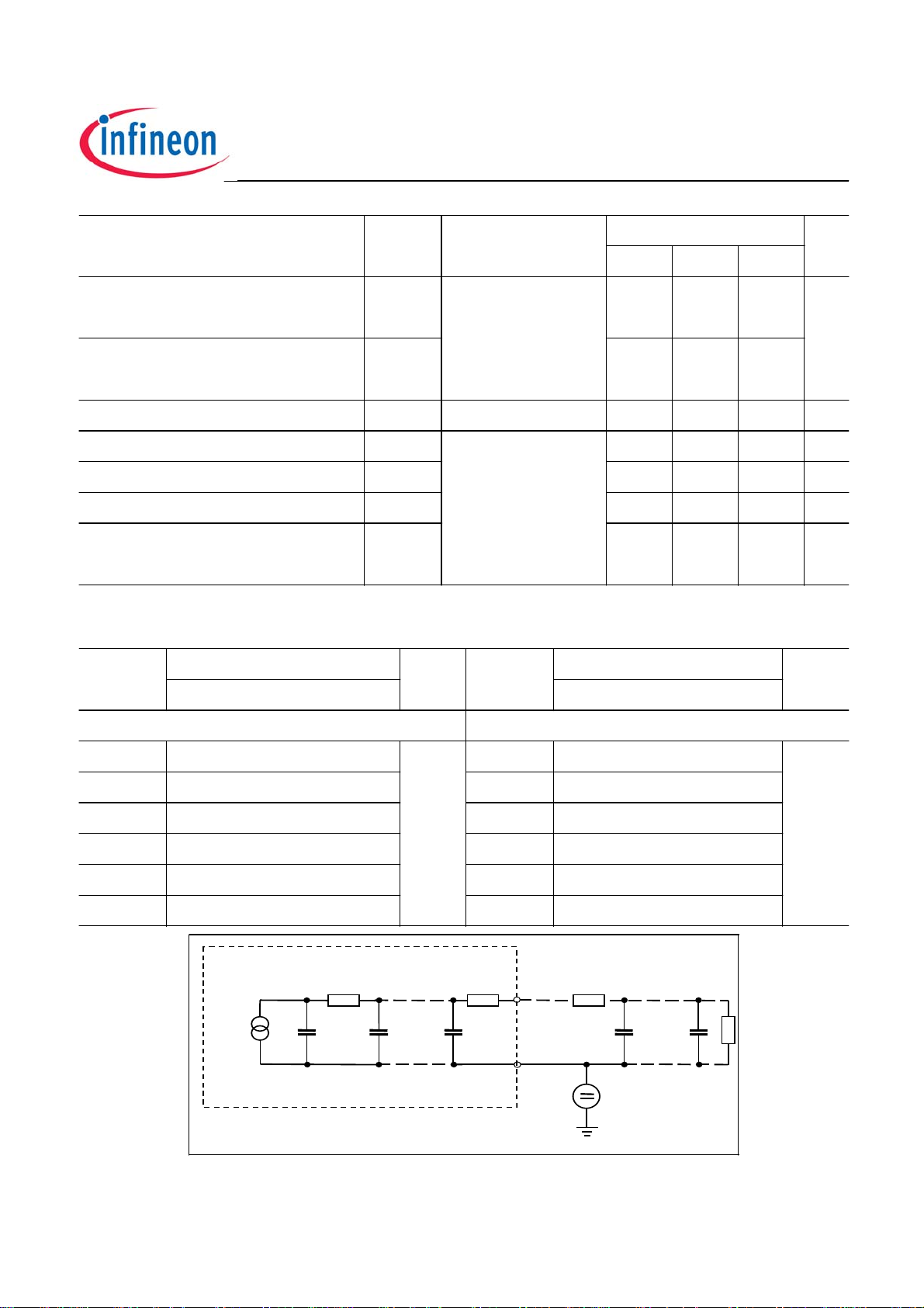
Definition of diodes switching characteristics
SPD06N80C3
Rev. 2.4 Page 9
2008-04-11

PG-TO252-3-1, PG-TO252-3-11, PG-TO252-3-21 (D-PAK)
SPD06N80C3
Rev. 2.4 Page 10
2008-04-11

SPD06N80C3
Rev. 2.4 Page 11
2008-04-11
 Loading...