

SPD06N60C3
CoolMOSTM Power Transistor
Features
• New revolutionary high voltage technology
• Ultra low gate charge
• Periodic avalanche rated
• High peak current capability
• Ultra low effective capacitances
• Extreme dv /dt rated
• Improved transconductance
Product Summary
VDS@ T
R
DS(on),max
I
D
j,max
650 V
0.75
6.2 A
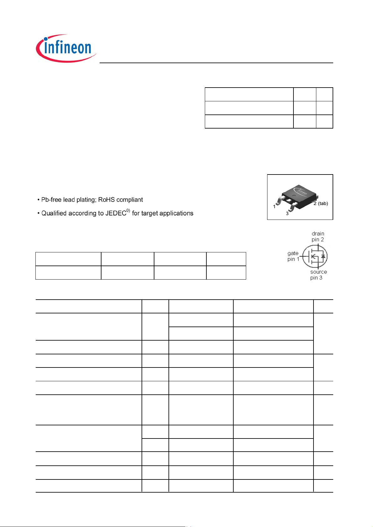
PG-TO252
Ω
Type Package Ordering Code Marking
SPD06N60C3 PG-TO252 Q67040-S4630 06N60C3
Maximum ratings, at T
Parameter Symbol Conditions Unit
Continuous drain current
Pulsed drain current
Avalanche energy, single pulse
Avalanche energy, repetitive t
Avalanche current, repetitive t
Drain source voltage slope dv /dt
Gate source voltage
=25 °C, unless otherwise specified
j
I
D
TC=25 °C
T
1)
AR
AR
1),2)
1)
I
D,pulse
E
AS
E
AR
I
AR
TC=25 °C
ID=3.1 A, VDD=50 V
ID=6.2 A, VDD=50 V
I
T
V
GS
static V
=100 °C
C
=6.2 A, VDS=480 V,
D
=125 °C
j
Value
6.2
3.9
18.6
200 mJ
0.5
6.2
50
±20
A
A
V/ns
V
GS
Power dissipation
Operating and storage temperature
Reverse diode dv/dt dv/dt 15 V/ns
7)
P
tot
T
, T
j
AC (f >1 Hz)
TC=25 °C
stg
±30
74
-55 ... 150
W
°C
Rev. 1.5 Page 1 2008-04-11

SPD06N60C3
Parameter Symbol Conditions Unit
Values
min. typ. max.
Thermal characteristics
Thermal resistance, junction - case
R
thJC
- - 1.7 K/W
SMD version, device
Thermal resistance, junction ambient
Soldering temperature *)
Electrical characteristics, at T
R
thJA
T
sold
=25 °C, unless otherwise specified
j
on PCB, minimal
footprint
SMD version, device
on PCB, 6 cm
3)
area
2
cooling
1.6 mm (0.063 in.)
from case for 10 s
--75
-50-
- - 260 °C
Static characteristics
Drain-source breakdown voltage
Avalanche breakdown voltage
Gate threshold voltage
Zero gate voltage drain current
Gate-source leakage current
Drain-source on-state resistance
Gate resistance
V
(BR)DSSVGS
V
(BR)DSVGS
V
GS(th)
I
DSS
I
GSS
R
DS(on)
R
G
=0 V, ID=250 µA
=0 V, ID=6.2 A
VDS=VGS, ID=0.26 mA
VDS=600 V, VGS=0 V,
T
=25 °C
j
=600 V, VGS=0 V,
V
DS
T
=150 °C
j
VGS=20 V, VDS=0 V
VGS=10 V, ID=3.9 A,
T
=25 °C
j
V
=10 V, ID=3.9 A,
GS
T
=150 °C
j
f =1 MHz, open drain
600 - - V
- 700 -
2.1 3 3.9
- 0.1 1 µA
- - 100
- - 100 nA
- 0.68 0.75
- 1.82 -
-1-
Ω
Transconductance
g
fs
|VDS|>2|ID|R
I
=3.9 A
D
DS(on)max
,
- 5.6 - S
*) reflow soldering, MSL3
Rev. 1.5 Page 2 2008-04-11
SPDT06N60C3
y
Parameter Symbol Conditions Unit
Values
min. typ. max.
namic characteristics
D
Input capacitance
Output capacitance
Reverse transfer capacitance
Effective output capacitance, energy
related
4)
Effective output capacitance, time
related
5)
Turn-on delay time
Rise time
Turn-off delay time
Fall time
C
C
C
C
C
t
t
t
t
iss
oss
rss
o(er)
o(tr)
d(on)
r
d(off)
f
=0 V, VDS=25 V,
V
GS
f =1 MHz
V
=0 V, VDS=0 V
GS
to 480 V
V
=480 V,
DD
V
=10 V, ID=6.2 A,
GS
R
=12 Ω
G
- 620 - pF
- 200 -
-17-
-28-
-47-
-7-ns
-12-
-52-
-10-
Gate Charge Characteristics
Gate to source charge
Gate to drain charge
Gate charge total
Gate plateau voltage
1)
Pulse width limited by maximum temperature T
2)
Repetitive avalanche causes additional power losses that can be calculated as PAV=EAR*f.
3)
Device on 40 mm x 40 mm x 1.5 mm epoxy PCB FR4 with 6 cm2 (one layer, 70 µm thick) copper area for drain
connection. PCB is vertical in still air.
4)
C
is a fixed capacitance that gives the same stored energy as C
o(er)
5)
C
is a fixed capacitance that gives the same charging time as C
o(tr)
7)
ISD<=ID, di/dt<=400A/us, V
Identical low-side and high-side switch.
DClink
Q
Q
Q
V
=400V, V
gs
gd
g
plateau
peak<VBR, DSS
j,max
V
DD
V
GS
only
=480 V, ID=6.2 A,
=0 to 10 V
while VDS is rising from 0 to 80% V
oss
while VDS is rising from 0 to 80% V
oss
, Tj<T
j,max
.
- 3.3 - nC
-12-
-2431
- 5.5 - V
DSS.
DSS.
Rev. 1.5 Page 3 2008-04-11
SPD06N60C3
y
Parameter Symbol Conditions Unit
Values
min. typ. max.
Reverse Diode
Diode continuous forward current
Diode pulse current
Diode forward voltage
Reverse recovery time
Reverse recovery charge
Peak reverse recovery current
T
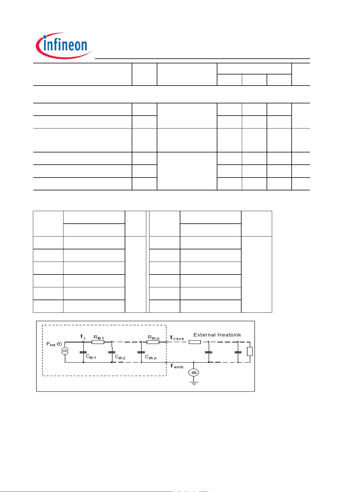
pical Transient Thermal Characteristics
I
S
I
S,pulse
V
SD
t
rr
Q
rr
I
rrm
T
=25 °C
C
VGS=0 V, IF=6.2 A,
T
=25 °C
j
=480 V, IF=IS,
V
R
di
/dt =100 A/µs
F
- - 6.2 A
- - 18.6
- 0.97 1.2 V
- 400 - ns
- 3.5 - µC
-25-A
Symbol Value Unit Symbol Value Unit
typ. typ.
R
th1
R
th2
R
th3
R
th4
R
th5
0.0325 K/W C
0.0448 C
0.251 C
0.31 C
0.231 C
th1
th2
th3
th4
th5
C
th6
0.0000502 Ws/K
0.000303
0.000428
0.00243
0.00344
6)
0.198
6)
C
models the additional heat capacitance of the package in case of non-ideal cooling. It is not needed if
th6
R
=0 K/W.
thCA
Rev. 1.5 Page 4 2008-04-11

1 Power dissipation 2 Safe operating area
P
=f(TC) ID=f(VDS); TC=25 °C; D =0
tot
parameter: t
p
SPD06N60C3
[A]
D
I
10
10
10
10
10
2
1
0
-1
-2
10
limited by on-state
resistance
0
10
1
VDS [V]
80
60
[W]
40
tot
P
20
0
0 40 80 120 160
TC [°C]
3 Max. transient thermal impedance 4 Typ. output characteristics
DC
10
2
10 µs
100 µs
10 ms
1 ms
1 µs
10
3
I
=f(VDS); Tj=25 °C ID=f(VDS); Tj=25 °C
D
parameter: D=t
1
10
/T parameter: V
p
20
GS
16
0.5
0
10
12
10
10
0.2
0.1
[A]
D
I
8
0.05
-1
0.02
0.01
single pulse
-2
10
10
-4
-5
-6
10
10
-3
10
-2
10
-1
10
0
4
0
0 5 10 15 20
[K/W]
thJC
Z
tp [s]
20 V
7 V
6.5 V
6 V
5.5 V
5 V
4.5 V
4 V
VDS [V]
Rev. 1.5 Page 5 2008-04-11

SPD06N60C3
5 Typ. output characteristics 6 Typ. drain-source on-state resistance
I
=f(VDS); Tj=150 °C R
D
parameter: V
GS
=f(ID); Tj=150 °C
DS(on)
parameter: V
GS
]
Ω
[
DS(on)
4
4 V
4.5 V
5 V
3
2
[A]
D
I
8
20 V
7 V
6.5 V
6 V
5.5 V
6
5 V
4
R
4.5 V
2
4 V
0
0 5 10 15 20
VDS [V]
1
0
0246810
ID [A]
7 Drain-source on-state resistance 8 Typ. transfer characteristics
5.5 V
6 V
20 V
R
=f(Tj); ID=3.9 A; VGS=10 V ID=f(VGS); |VDS|>2|ID|R
DS(on)
parameter: T
2
1.6
1.2
]
Ω
[
98 %
typ
R
DS(on)
0.8
0.4
0
-60 -20 20 60 100 140 180
Tj [°C]
[A]
D
I
25
20
15
10
5
0
DS(on)max
j
25 °C
150 °C
0246810
VGS [V]
Rev. 1.5 Page 6 2008-04-11

SPD06N60C3
9 Typ. gate charge 10 Forward characteristics of reverse diode
V
=f(Q
GS
parameter: V
); ID=6.2 A pulsed IF=f(VSD)
gate
DD
parameter: T
j
12
10
2
10
[V]
GS
V
120 V
8
6
4
480 V
[A]
F
I
10
10
1
150 °C
0
2
-1
0
0102030
Q
[nC]
gate
10
0 0.5 1 1.5 2 2.5
11 Avalanche SOA 12 Avalanche energy
25 °C
VSD [V]
25 °C, 98%
150 °C, 98%
I
=f(tAR) EAS=f(Tj); ID=3.1 A; VDD=50 V
AR
parameter: T
j(start)
8
250
200
6
150
[A]
4
AV
I
125 °C 25 °C
[mJ]
AS
E
100
2
50
0
10
10
-2
-3
10
-1
10
0
10
1
10
2
10
3
0
20 60 100 140 180
tAR [µs]
Tj [°C]
Rev. 1.5 Page 7 2008-04-11

13 Drain-source breakdown voltage 14 Typ. capacitances
SPD06N60C3
V
BR(DSS)
=f(Tj); ID=0.25 mA C =f(VDS); VGS=0 V; f =1 MHz
700
660
[V]
620
BR(DSS)
V
580
540
-60 -20 20 60 100 140 180
Tj [°C]
4
10
3
10
2
10
[pF]
C
1
10
0
10
0 100 200 300 400 500
Ciss
Coss
Crss
VDS [V]
15 Typ. C
E
= f(VDS)
oss
5
4
3
[µJ]
oss
E
2
1
0
stored energy
oss
0 100 200 300 400 500 600
VDS [V]
Rev. 1.5 Page 8 2008-04-11

Definition of diode switching characteristics
SPD06N60C3
Rev. 1.5 Page 9 2008-04-11

PG-TO252-3-1: Outline , PG-TO-252-3-11 (D-PAK), PG-TO-252-3-21 (D-PAK)
SPD06N60C3
Rev. 1.5 Page 10 2008-04-11

SPD06N60C3
Rev. 1.5 Page 11 2008-04-11
 Loading...