

Page 1

Data Sheet Please read the Important Notice and Warnings at the end of this document Revision 1.2
www.infineon.com 2020-05-14
SP400-11-01
SP40PLUS
Tire Pressure Monitoring Sensor
Quality Requirement Category: Automotive
Features
• Patented Glass-Silicon-Glass MEMS pressure sensor with best-in-class media compatibility
• Calibrated pressure sensor for absolute air pressure measurement
• Z-axis accelerometer for motion detection and angular measurement
• Temperature and supply voltage sensors
• Industry-standard 8051 microcontroller with 12K of Flash memory
• System Controller with flexible wake-up and power management features
• RF Transmitter with fractional-N sigma-delta PLL
• Unique firmware functions for determination of angular wheel position, supporting tire localization (APS)
• LF Receiver allows carrier detection and modulated telegram reception
Applications
• Valve based TPMS-Modules
•OEM
•Aftermarket
•Retrofit
• In Tire TPMS Modules
Description
The SP40PLUS provides a very high level of integration, and is optimized to perform all of the functions necessary
to implement a state-of-the-art Tire Pressure Monitoring System (TPMS) sensor module. With its integrated micro
controller, sensors, and convenient peripherals, the SP40PLUS needs the addition of only a few passive
components and a battery to form a complete TPMS sensor assembly.
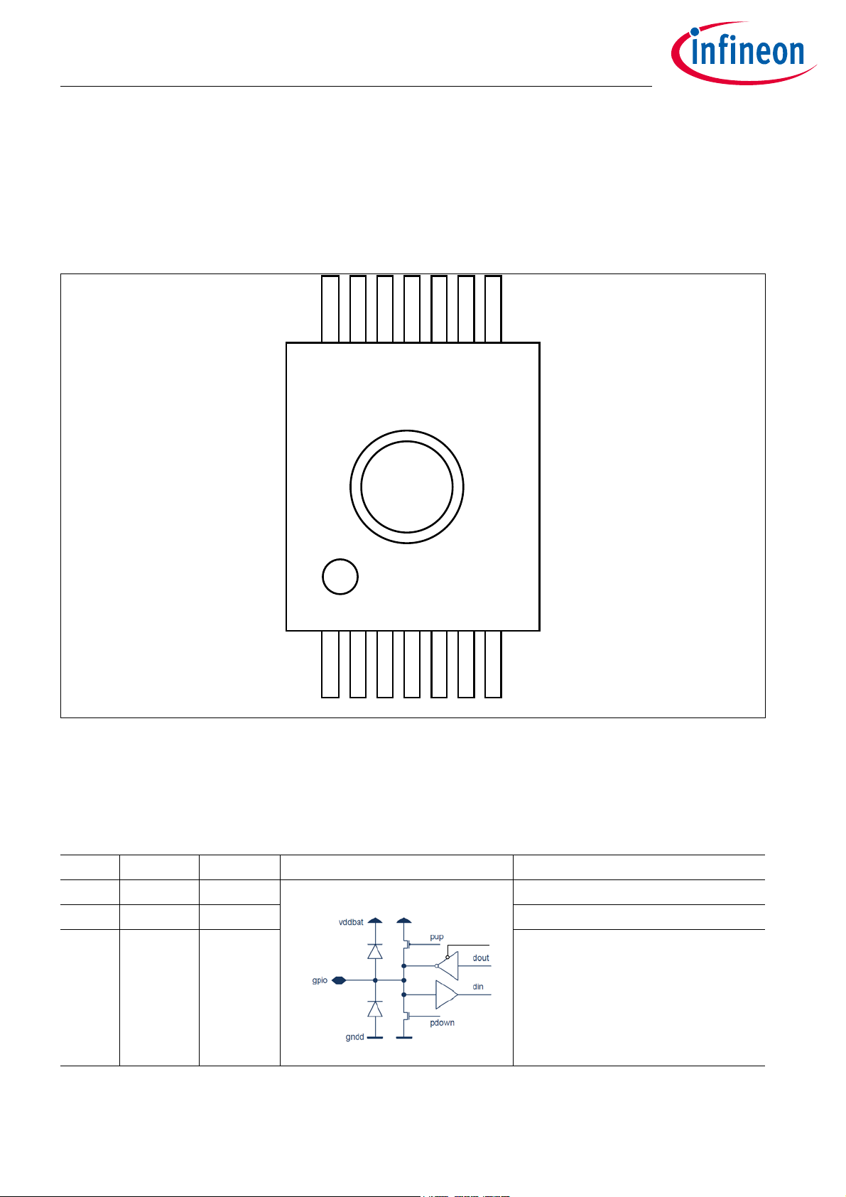
Figure 1
PG-DSOSP-14-82
Page 2

SP40PLUS
Tire Pressure Monitoring Sensor
Table of Contents
Features . . . . . . . . . . . . . . . . . . . . . . . . . . . . . . . . . . . . . . . . . . . . . . . . . . . . . . . . . . . . . . . . . . . . . . . . . . . 1
Applications . . . . . . . . . . . . . . . . . . . . . . . . . . . . . . . . . . . . . . . . . . . . . . . . . . . . . . . . . . . . . . . . . . . . . . . . 1
Description . . . . . . . . . . . . . . . . . . . . . . . . . . . . . . . . . . . . . . . . . . . . . . . . . . . . . . . . . . . . . . . . . . . . . . . . 1
Table of Contents . . . . . . . . . . . . . . . . . . . . . . . . . . . . . . . . . . . . . . . . . . . . . . . . . . . . . . . . . . . . . . . . . . . 2
1 Introduction . . . . . . . . . . . . . . . . . . . . . . . . . . . . . . . . . . . . . . . . . . . . . . . . . . . . . . . . . . . . . . . . . . . . . . . 4
2 Specification . . . . . . . . . . . . . . . . . . . . . . . . . . . . . . . . . . . . . . . . . . . . . . . . . . . . . . . . . . . . . . . . . . . . . . . 5
2.1 Absolute Maximum Ratings . . . . . . . . . . . . . . . . . . . . . . . . . . . . . . . . . . . . . . . . . . . . . . . . . . . . . . . . . . . . . . . . . . . 5
2.2 Operating Range . . . . . . . . . . . . . . . . . . . . . . . . . . . . . . . . . . . . . . . . . . . . . . . . . . . . . . . . . . . . . . . . . . . . . . . . . . . . 7
2.3 Characteristics . . . . . . . . . . . . . . . . . . . . . . . . . . . . . . . . . . . . . . . . . . . . . . . . . . . . . . . . . . . . . . . . . . . . . . . . . . . . . . 8
2.3.1 Pressure Sensor . . . . . . . . . . . . . . . . . . . . . . . . . . . . . . . . . . . . . . . . . . . . . . . . . . . . . . . . . . . . . . . . . . . . . . . . . . . 8
2.3.2 z-axis Acceleration Sensor . . . . . . . . . . . . . . . . . . . . . . . . . . . . . . . . . . . . . . . . . . . . . . . . . . . . . . . . . . . . . . . . . . 9
2.3.3 Temperature Sensor . . . . . . . . . . . . . . . . . . . . . . . . . . . . . . . . . . . . . . . . . . . . . . . . . . . . . . . . . . . . . . . . . . . . . . 10
2.3.4 Battery Sensor . . . . . . . . . . . . . . . . . . . . . . . . . . . . . . . . . . . . . . . . . . . . . . . . . . . . . . . . . . . . . . . . . . . . . . . . . . . 10
2.3.5 Thermal Shutdown . . . . . . . . . . . . . . . . . . . . . . . . . . . . . . . . . . . . . . . . . . . . . . . . . . . . . . . . . . . . . . . . . . . . . . . 10
2.3.6 General Purpose Digital I/O Pins . . . . . . . . . . . . . . . . . . . . . . . . . . . . . . . . . . . . . . . . . . . . . . . . . . . . . . . . . . . 11
2.3.7 Voltage Monitoring and Power On . . . . . . . . . . . . . . . . . . . . . . . . . . . . . . . . . . . . . . . . . . . . . . . . . . . . . . . . . . 12
2.3.8 Flash memory . . . . . . . . . . . . . . . . . . . . . . . . . . . . . . . . . . . . . . . . . . . . . . . . . . . . . . . . . . . . . . . . . . . . . . . . . . . . 12
2.3.9 Supply Currents . . . . . . . . . . . . . . . . . . . . . . . . . . . . . . . . . . . . . . . . . . . . . . . . . . . . . . . . . . . . . . . . . . . . . . . . . . 13
2.3.10 LF-Receiver . . . . . . . . . . . . . . . . . . . . . . . . . . . . . . . . . . . . . . . . . . . . . . . . . . . . . . . . . . . . . . . . . . . . . . . . . . . . . . 14
2.3.11 RF-Transmitter . . . . . . . . . . . . . . . . . . . . . . . . . . . . . . . . . . . . . . . . . . . . . . . . . . . . . . . . . . . . . . . . . . . . . . . . . . . 15
2.3.12 RC Oscillators . . . . . . . . . . . . . . . . . . . . . . . . . . . . . . . . . . . . . . . . . . . . . . . . . . . . . . . . . . . . . . . . . . . . . . . . . . . . 16
2.3.13 Wake-up and power-on timing . . . . . . . . . . . . . . . . . . . . . . . . . . . . . . . . . . . . . . . . . . . . . . . . . . . . . . . . . . . . . 16
3 Pin Description . . . . . . . . . . . . . . . . . . . . . . . . . . . . . . . . . . . . . . . . . . . . . . . . . . . . . . . . . . . . . . . . . . . . 18
3.1 Pin Configuration . . . . . . . . . . . . . . . . . . . . . . . . . . . . . . . . . . . . . . . . . . . . . . . . . . . . . . . . . . . . . . . . . . . . . . . . . . 18
3.2 Pin Description . . . . . . . . . . . . . . . . . . . . . . . . . . . . . . . . . . . . . . . . . . . . . . . . . . . . . . . . . . . . . . . . . . . . . . . . . . . . . 18
4 Special Features of the SP40PLUS . . . . . . . . . . . . . . . . . . . . . . . . . . . . . . . . . . . . . . . . . . . . . . . . . . . . 21
4.1 Operating Modes . . . . . . . . . . . . . . . . . . . . . . . . . . . . . . . . . . . . . . . . . . . . . . . . . . . . . . . . . . . . . . . . . . . . . . . . . . . 21
4.2 Device states . . . . . . . . . . . . . . . . . . . . . . . . . . . . . . . . . . . . . . . . . . . . . . . . . . . . . . . . . . . . . . . . . . . . . . . . . . . . . . . 21
4.3 State Transitions . . . . . . . . . . . . . . . . . . . . . . . . . . . . . . . . . . . . . . . . . . . . . . . . . . . . . . . . . . . . . . . . . . . . . . . . . . . 22
5 Functional Descriptions . . . . . . . . . . . . . . . . . . . . . . . . . . . . . . . . . . . . . . . . . . . . . . . . . . . . . . . . . . . . 25
5.1 SP40PLUS Block Diagram . . . . . . . . . . . . . . . . . . . . . . . . . . . . . . . . . . . . . . . . . . . . . . . . . . . . . . . . . . . . . . . . . . . 25
5.2 Wake-up Controller . . . . . . . . . . . . . . . . . . . . . . . . . . . . . . . . . . . . . . . . . . . . . . . . . . . . . . . . . . . . . . . . . . . . . . . . . 25
5.2.1 Interval Timer . . . . . . . . . . . . . . . . . . . . . . . . . . . . . . . . . . . . . . . . . . . . . . . . . . . . . . . . . . . . . . . . . . . . . . . . . . . . 26
5.2.2 LF ON-OFF Timer . . . . . . . . . . . . . . . . . . . . . . . . . . . . . . . . . . . . . . . . . . . . . . . . . . . . . . . . . . . . . . . . . . . . . . . . . 27
5.2.3 LF receiver wake-up/resume events . . . . . . . . . . . . . . . . . . . . . . . . . . . . . . . . . . . . . . . . . . . . . . . . . . . . . . . . 27
5.2.4 General purpose I/O PP2 wake-up/resume event . . . . . . . . . . . . . . . . . . . . . . . . . . . . . . . . . . . . . . . . . . . . 27
5.2.5 Power-on and under-voltage reset . . . . . . . . . . . . . . . . . . . . . . . . . . . . . . . . . . . . . . . . . . . . . . . . . . . . . . . . . 28
5.2.6 Software reset, watchdog reset and flash error reset . . . . . . . . . . . . . . . . . . . . . . . . . . . . . . . . . . . . . . . . . 28
5.2.7 Thermal Shutdown . . . . . . . . . . . . . . . . . . . . . . . . . . . . . . . . . . . . . . . . . . . . . . . . . . . . . . . . . . . . . . . . . . . . . . . 29
5.3 System Controller . . . . . . . . . . . . . . . . . . . . . . . . . . . . . . . . . . . . . . . . . . . . . . . . . . . . . . . . . . . . . . . . . . . . . . . . . . 29
5.3.1 Sampling Timer . . . . . . . . . . . . . . . . . . . . . . . . . . . . . . . . . . . . . . . . . . . . . . . . . . . . . . . . . . . . . . . . . . . . . . . . . . 30
5.4 Clock Generators . . . . . . . . . . . . . . . . . . . . . . . . . . . . . . . . . . . . . . . . . . . . . . . . . . . . . . . . . . . . . . . . . . . . . . . . . . . 31
5.5 Core . . . . . . . . . . . . . . . . . . . . . . . . . . . . . . . . . . . . . . . . . . . . . . . . . . . . . . . . . . . . . . . . . . . . . . . . . . . . . . . . . . . . . . 32
5.5.1 Timer Module . . . . . . . . . . . . . . . . . . . . . . . . . . . . . . . . . . . . . . . . . . . . . . . . . . . . . . . . . . . . . . . . . . . . . . . . . . . . 33
5.5.2 Watchdog . . . . . . . . . . . . . . . . . . . . . . . . . . . . . . . . . . . . . . . . . . . . . . . . . . . . . . . . . . . . . . . . . . . . . . . . . . . . . . . . 34
Data Sheet 2 Revision 1.2
2020-05-14
Page 3

SP40PLUS
Tire Pressure Monitoring Sensor
5.5.3 Hardware CRC . . . . . . . . . . . . . . . . . . . . . . . . . . . . . . . . . . . . . . . . . . . . . . . . . . . . . . . . . . . . . . . . . . . . . . . . . . . . 35
5.5.4 I2C Controller . . . . . . . . . . . . . . . . . . . . . . . . . . . . . . . . . . . . . . . . . . . . . . . . . . . . . . . . . . . . . . . . . . . . . . . . . . . . . 35
5.5.5 UART Interface . . . . . . . . . . . . . . . . . . . . . . . . . . . . . . . . . . . . . . . . . . . . . . . . . . . . . . . . . . . . . . . . . . . . . . . . . . . 37
5.6 Memories . . . . . . . . . . . . . . . . . . . . . . . . . . . . . . . . . . . . . . . . . . . . . . . . . . . . . . . . . . . . . . . . . . . . . . . . . . . . . . . . . . 38
5.6.1 Lock-byte concept overview . . . . . . . . . . . . . . . . . . . . . . . . . . . . . . . . . . . . . . . . . . . . . . . . . . . . . . . . . . . . . . . 38
5.6.2 Flash programming . . . . . . . . . . . . . . . . . . . . . . . . . . . . . . . . . . . . . . . . . . . . . . . . . . . . . . . . . . . . . . . . . . . . . . . 39
5.6.3 Retention RAM . . . . . . . . . . . . . . . . . . . . . . . . . . . . . . . . . . . . . . . . . . . . . . . . . . . . . . . . . . . . . . . . . . . . . . . . . . . 39
5.6.4 Data RAM and SFRs . . . . . . . . . . . . . . . . . . . . . . . . . . . . . . . . . . . . . . . . . . . . . . . . . . . . . . . . . . . . . . . . . . . . . . . 39
5.6.5 Retention SFRs . . . . . . . . . . . . . . . . . . . . . . . . . . . . . . . . . . . . . . . . . . . . . . . . . . . . . . . . . . . . . . . . . . . . . . . . . . . 40
5.7 Power Supply and Reset Generator . . . . . . . . . . . . . . . . . . . . . . . . . . . . . . . . . . . . . . . . . . . . . . . . . . . . . . . . . . 40
5.7.1 TX battery voltage detector . . . . . . . . . . . . . . . . . . . . . . . . . . . . . . . . . . . . . . . . . . . . . . . . . . . . . . . . . . . . . . . . 40
5.8 Measurement Interface . . . . . . . . . . . . . . . . . . . . . . . . . . . . . . . . . . . . . . . . . . . . . . . . . . . . . . . . . . . . . . . . . . . . . 41
5.9 RF transmitter . . . . . . . . . . . . . . . . . . . . . . . . . . . . . . . . . . . . . . . . . . . . . . . . . . . . . . . . . . . . . . . . . . . . . . . . . . . . . 41
5.9.1 Manchester/Biphase Encoder . . . . . . . . . . . . . . . . . . . . . . . . . . . . . . . . . . . . . . . . . . . . . . . . . . . . . . . . . . . . . . 42
5.9.2 SD-PLL . . . . . . . . . . . . . . . . . . . . . . . . . . . . . . . . . . . . . . . . . . . . . . . . . . . . . . . . . . . . . . . . . . . . . . . . . . . . . . . . . . 43
5.9.3 FSK Modulator . . . . . . . . . . . . . . . . . . . . . . . . . . . . . . . . . . . . . . . . . . . . . . . . . . . . . . . . . . . . . . . . . . . . . . . . . . . 44
5.9.4 Gaussian filter . . . . . . . . . . . . . . . . . . . . . . . . . . . . . . . . . . . . . . . . . . . . . . . . . . . . . . . . . . . . . . . . . . . . . . . . . . . 44
5.9.5 RF Power Amplifier . . . . . . . . . . . . . . . . . . . . . . . . . . . . . . . . . . . . . . . . . . . . . . . . . . . . . . . . . . . . . . . . . . . . . . . 45
5.9.6 ASK modulator and ASK ramping . . . . . . . . . . . . . . . . . . . . . . . . . . . . . . . . . . . . . . . . . . . . . . . . . . . . . . . . . . . 45
5.9.7 Crystal Oscillator . . . . . . . . . . . . . . . . . . . . . . . . . . . . . . . . . . . . . . . . . . . . . . . . . . . . . . . . . . . . . . . . . . . . . . . . . 46
5.9.8 RF Baud-Rate Generator . . . . . . . . . . . . . . . . . . . . . . . . . . . . . . . . . . . . . . . . . . . . . . . . . . . . . . . . . . . . . . . . . . . 47
5.10 RF Transmission Controller . . . . . . . . . . . . . . . . . . . . . . . . . . . . . . . . . . . . . . . . . . . . . . . . . . . . . . . . . . . . . . . . . . 47
5.10.1 SOM and EOM Feature . . . . . . . . . . . . . . . . . . . . . . . . . . . . . . . . . . . . . . . . . . . . . . . . . . . . . . . . . . . . . . . . . . . . 49
5.10.2 Voltage measurement at end of transmission . . . . . . . . . . . . . . . . . . . . . . . . . . . . . . . . . . . . . . . . . . . . . . . 50
5.11 LF Receiver . . . . . . . . . . . . . . . . . . . . . . . . . . . . . . . . . . . . . . . . . . . . . . . . . . . . . . . . . . . . . . . . . . . . . . . . . . . . . . . . 50
5.11.1 LF Analog Front End (AFE) . . . . . . . . . . . . . . . . . . . . . . . . . . . . . . . . . . . . . . . . . . . . . . . . . . . . . . . . . . . . . . . . . 51
5.11.2 LF Digital baseband (DBB) . . . . . . . . . . . . . . . . . . . . . . . . . . . . . . . . . . . . . . . . . . . . . . . . . . . . . . . . . . . . . . . . . 51
5.11.3 LF Telegram . . . . . . . . . . . . . . . . . . . . . . . . . . . . . . . . . . . . . . . . . . . . . . . . . . . . . . . . . . . . . . . . . . . . . . . . . . . . . . 54
5.11.4 LF state machine . . . . . . . . . . . . . . . . . . . . . . . . . . . . . . . . . . . . . . . . . . . . . . . . . . . . . . . . . . . . . . . . . . . . . . . . . 54
5.12 I/O-Port . . . . . . . . . . . . . . . . . . . . . . . . . . . . . . . . . . . . . . . . . . . . . . . . . . . . . . . . . . . . . . . . . . . . . . . . . . . . . . . . . . . 58
6 Application Circuit . . . . . . . . . . . . . . . . . . . . . . . . . . . . . . . . . . . . . . . . . . . . . . . . . . . . . . . . . . . . . . . . . 59
7 Data Sheet Reference Board . . . . . . . . . . . . . . . . . . . . . . . . . . . . . . . . . . . . . . . . . . . . . . . . . . . . . . . . . 61
8 Package Information . . . . . . . . . . . . . . . . . . . . . . . . . . . . . . . . . . . . . . . . . . . . . . . . . . . . . . . . . . . . . . . 65
8.1 Package Outline . . . . . . . . . . . . . . . . . . . . . . . . . . . . . . . . . . . . . . . . . . . . . . . . . . . . . . . . . . . . . . . . . . . . . . . . . . . . 65
8.2 Marking . . . . . . . . . . . . . . . . . . . . . . . . . . . . . . . . . . . . . . . . . . . . . . . . . . . . . . . . . . . . . . . . . . . . . . . . . . . . . . . . . . . 66
8.3 Package axis definition . . . . . . . . . . . . . . . . . . . . . . . . . . . . . . . . . . . . . . . . . . . . . . . . . . . . . . . . . . . . . . . . . . . . . 67
References . . . . . . . . . . . . . . . . . . . . . . . . . . . . . . . . . . . . . . . . . . . . . . . . . . . . . . . . . . . . . . . . . . . . . . . . 69
Terminology . . . . . . . . . . . . . . . . . . . . . . . . . . . . . . . . . . . . . . . . . . . . . . . . . . . . . . . . . . . . . . . . . . . . . . 70
Data Sheet 3 Revision 1.2
2020-05-14
Page 4

SP40PLUS
Tire Pressure Monitoring Sensor
Introduction
1 Introduction
Measurements of pressure, acceleration, temperature, and battery voltage are performed under software
control, allowing the application software to format and prepare the data for RF transmission. An intelligent
system controller provides flexible wake-up capability in order to reduce energy usage. A calibrated Interval
Timer is included to permit periodic wake-up of the CPU, which in turn can then perform measurements and
transmit data to a receiver. The integrated Z-axis accelerometer may be used by the application software to
detect motion and distinguish between parking and driving situation.
The integrated microcontroller is instruction set compatible to the standard 8051 processor and is supported by
commercially available C compilers and IDE tool chains. The microcontroller core is supplemented with various
peripherals (e.g. hardware Manchester/BiPhase Encoder/Decoder, CRC Generator/Checker, I2C- and UARTinterface) that enable an easy implementation of TPMS application software.
For user specific application code the SP40PLUS includes 12k of on-chip flash memory.
The RF Transmitter block covers both 315 and 434 MHz UHF bands and supports FSK and ASK modulation. The
transmitter contains a fractional-N sigma-delta PLL synthesizer which allows for precise control of carrier
frequency and accurate FSK frequency modulation. A flexible baseband encoder and advanced power
management techniques are used to hold the peak current consumption during RF transmission to a minimum.
An integrated autonomous LF Receiver allows the SP40PLUS to receive diagnostic or operating state commands,
supporting application features such as pressure-on-demand or tire position localization.
Finally, a comprehensive firmware library supports using all above mentioned hardware blocks effectively.
Especially a unique set of Angular Position Sensing (APS) functions allows calculating the instantaneous angular
position of the TPMS module relative to the car chassis which may be used for wheel localization on system level.
Data Sheet 4 Revision 1.2
2020-05-14
Page 5

SP40PLUS
Tire Pressure Monitoring Sensor
Specification
2 Specification
2.1 Absolute Maximum Ratings
Table 1 Absolute Maximum Ratings
Parameter Symbol Values Unit Note or Test Condition Number
Min. Typ. Max.
Max. Supply Voltage V
ESD robustness HBM V
ESD robustness CDM V
Latch up I
Input voltage V
Peak voltage at
PAOUT pin
DDmax
ESD_HBM
ESD_CDM
LU
In
V
In_LF
V
PAOUT_peak
-0.3 +3.8 V 1.1
-2000 2000 V All pins according to
1.2
EIA/JESD22-A114-B
-4000 4000 V PAOUT pin according to
1.3
EIA/JESD22-A114-B
-500 500 V All pins (According to ESDA
1.4
STM 5.3.1)
-750 750 V Corner pins (According to
1.5
ESDA STM 5.3.1)
-100 +100 mA AEC-Q100 (transient
1.6
current)
-0.3 VDD +
V PP0, PP1, PP2, PP3 1.7
0.3
-0.3 +1.8 V LFP, LFN, XIN 1.8
-0.3 +0.3 V Differential input at LFP
1.9
and LFN
8 V The matching network
1.10
must be designed such
that the peak-voltage at PA
does not exceed this value
Output short-circuit
capability
1)
V
SC
0 3.8 V Short to VDD, GND or
neighbor pin for max.
1.11
10min at VDD=3.8V. Note:
VDDREG and XOUT must
not be shorted to VDD
DC current I
Over pressure p
Burst pressure p
Static acceleration a
DC
max
burst
static
-10 10 mA all pins 1.13
2000 kPa static load 1.14
2000 kPa 10 times 1 sec 1.15
3000 g Device unpowered. Tested
1.16
in z-direction.
Data Sheet 5 Revision 1.2
2020-05-14
Page 6

SP40PLUS
Tire Pressure Monitoring Sensor
Specification
Table 1 Absolute Maximum Ratings
Parameter Symbol Values Unit Note or Test Condition Number
Min. Typ. Max.
Mechanical shock a
shock
6000 g 0.3 ms half sine pulses.
1.17
5 shocks in +/- x,y,zdirection, respectively.
Device unpowered.
Storage temperature T
storage
-50 +150 °C Maximal 1000 hours
1.18
accumulated over
lifetime between 125°C
and 150°C. Device not
powered. Temperature
cycling only allowed
between -40°C and 125°C.
1) Refers to following pins: PP0 to PP3 if configured as output, XOUT, VDDREG, PAOUT and VDDPA. For input pins see
parameter input voltage.
Note: Absolute maximum ratings are values beyond recommended operating conditions. They describe
those conditions which the device can withstand for some limited time. After exposure to
maximum ratings the device will remain functional, but the reliability is no longer guaranteed.
Data Sheet 6 Revision 1.2
2020-05-14
Page 7

SP40PLUS
Tire Pressure Monitoring Sensor
Specification
2.2 Operating Range
The operating range defines the ambient conditions where the device operates as specified. Certain specified
parameters in this data sheet may depend on additional operating conditions. These additional conditions are
indicated in the corresponding sections.
Table 2 Operating Range
Parameter Symbol Values Unit Note or
Test Condition
Supply Voltage
Min. Typ. Max.
1)
V
DD
VUVRA – 3.6 V Device not in power
down state
VUVRPD – 3.6 V Device in power down
state
Ambient Temperature T
Operating
T
Flash
-40 – 125 °C Normal Operation 3.3
-20 – 90 °C FLASH
programming/erasing
Extended
Temperature Range
T
EXT
-50 150 °C Thermal shutdown
functional. V
to 3.6 V. Exposure to
125°C...150°C maximal
24h over lifetime
z-axis Acceleration a
Operating
-1600 – 1600 g Exceeding this
acceleration will result
in a higher pressure
error as specified.
1) Supply voltage must be connected to VDDBAT pin.
DD
= V
UVRA
Number
3.1
3.2
3.4
3.5
3.6
Data Sheet 7 Revision 1.2
2020-05-14
Page 8

SP40PLUS
Tire Pressure Monitoring Sensor
Specification
2.3 Characteristics
2.3.1 Pressure Sensor
Table 3 Pressure Sensor 500/750/900kPa Variant
1)2)
Parameter Symbol Values Unit Note or Test Condition Number
Min. Typ. Max.
Input Pressure Range p
Random Error p
ADC resolution p
Measurement Error
3)
in
random
ADC_res
p
Error 100-500
100 900 kPa 7.1
-1.37 1.37 kPa 95% of all measurements 7.2
0.5 kPa/
LSB
1 LSB of a raw measurement
corresponds to 0.5 kPa or less
7.3
-5 5 kPa 0°C to +90°C 7.4
-7 7 kPa -20°C to 0°C
7.5
+90°C to +125°C
-9 9 kPa -40°C to -20°C 7.6
p
Error 500-750
-1.2 1.2 %
-1.6 1.6 %
4)
0°C to +90°C 7.7
4)
-20°C to 0°C
7.8
+90°C to +125°C
4)
-40°C to -20°C 7.9
p
Error 750-900
-2.0 2.0 %
-12 12 kPa 0°C to +125°C 7.10
-14 14 kPa -20°C to 0°C 7.11
-15 15 kPa -40°C to -20°C 7.12
1) Based on averaging two raw values for each measurement
2) Exceeding the maximum z-axis acceleration (parameter 3.6) as defined in the operating range will result in a higher
pressure measurement error than specified
3) The measurement error is understood as total error, including random error (noise)
4) Percentage of actual pressure value
Data Sheet 8 Revision 1.2
2020-05-14
Page 9

SP40PLUS
Tire Pressure Monitoring Sensor
Specification
2.3.2 z-axis Acceleration Sensor
Table 4 z-axis Acceleration Sensor
Parameter Symbol Values Unit Note or Test Condition Number
Min. Typ. Max.
Input acceleration
Range
Total Acceleration
1)
Error
Random error of
acceleration
compensated values
a
in
a
err_tot
a
rnd_comp_
16
-20 355 g Selectable by firmware function 12.1
-355 20 g 12.2
-6.5
(-3.0)
-8.5
(-5.0)
-8.5
(-5.0)
-10.5
(-7.0)
-12.5
(-9.0)
-14.5
(-11.0)
-22.5
(-19.0)
-24
(-20.5)
-0.35 +0.35 g 99.7% of all measurements.
+6.5
(+3.0)
+8.5
(+5.0)
+8.5
(+5.0)
+10.5
(+7.0)
+12.5
(+9.0)
+14.5
(+11.0)
+22.5
(+19.0)
+24
(+20.5)
g|a
T = -40°C...90°C
g|a
T = 90°C...125°C
g|a
T = -40°C...90°C
g|a
T = 90°C...125°C
g|a
T = -40°C...90°C
g|a
T = 90°C...125°C
g|a
T = -40°C...90°C
g|a
T = 90°C...125°C
|=0g ... 20g
in
|=0g ... 20g
in
|>20g ... 100g
in
|>20g ... 100g
in
|>100g ... 200g
in
|>100g ... 200g
in
|>200g ... 355g
in
|>200g ... 355g
in
12.3
12.4
12.5
12.6
12.7
12.8
12.9
12.10
12.11
Averaging of 16 ADC-samples.
No external noise sources present.
ADC resolution a
ADC_res
0.057 0.175 g/
1 LSB of a raw measurement
LSB
corresponds to minimal 0.057g and
12.14
maximal 0.175g
Random error of
acceleration raw
values
Accelerometer
resonance frequency
a
rnd_raw_16
f
res_acc
-4 +4 LSB 99.7% of all measurements.
Averaging of 16 ADC-samples.
No external noise sources present.
5.1 6 6.9 kHz Mechanical excitation of the
SP40PLUS in this frequency range
12.16
12.17
must be avoided (e.g. PCB sawing
process)
1) Total error specifications are based on averaging 16 raw values for each measurement and they include random error
(noise). The total error may be reduced by 3.5g by periodically (e.g. every 3 months) using the automatic acceleration
offset compensation function Lib_Comp_Auto_Acc_Offset(). The reduced errors are put into brackets.
Data Sheet 9 Revision 1.2
2020-05-14
Page 10

SP40PLUS
Tire Pressure Monitoring Sensor
Specification
2.3.3 Temperature Sensor
Table 5 Temperature Sensor
Parameter Symbol Values Unit Note or Test Condition Number
Min. Typ. Max.
Measurement range T
Measurement error
1)
Random error T
range
T
Error
random
-40 +125 °C 14.1
-3 +3 °C 14.2
-1 +1 °C 95% of all
14.4
measurements
1) The measurement error is understood as total error, including random error (noise)
2.3.4 Battery Sensor
Table 6 Battery Sensor
Parameter Symbol Values Unit Note or Test Condition Number
Min. Typ. Max.
Measurement range V
Measurement error
1)
V
range
Error
VUVRA 3.6 V see Table 10 for V
-3 – +3 % percentage of
UVRA
15.1
15.2
measurement value
1) The measurement error is understood as total error, including random error (noise)
2.3.5 Thermal Shutdown
Table 7 Thermal Shutdown
Parameter Symbol Values Unit Note or Test Condition Number
Min. Typ. Max.
Thermal Shutdown
T
HOT TH
119 122 125 °C 16.1
HOT threshold
Thermal Shutdown
T
HOT RE
115 120 123.5 °C 16.2
HOT release
Hysteresis T
Thermal Shutdown
HYST
T
COLD TH
1.5 4 °C 16.3
-40 -37 -34 °C 16.4
COLD threshold
Thermal Shutdown
T
COLD RE
-38.5 -35 -30 °C 16.5
COLD release
Data Sheet 10 Revision 1.2
2020-05-14
Page 11

SP40PLUS
Tire Pressure Monitoring Sensor
Specification
2.3.6 General Purpose Digital I/O Pins
Table 8 Digital I/O Pins - Operating Range
Parameter Symbol Values Unit Note or Test Condition Number
Min. Typ. Max.
Digital Pin Output
I
out DIG
-4 4 mA Pins PP0 to PP3 17.1
Current
Digital Pin Input High
Voltage
Digital Pin Input Low
Voltage
V
IH
V
IL
0.8V
DD
V
- 0.05 V for lowest current
DD
0.2V
50 mV for lowest current
V functional 17.2
consumption
V functional 17.4
DD
1)
17.3
17.5
consumption
1) If the digital I/O pins are left open and the internal pull resistors are activated the +/-50mV criterion is fulfilled
Table 9 Digital I/O Pins - Electrical Characteristics
Parameter Symbol Values Unit Note or Test Condition Number
Min. Typ. Max.
Digital Pin-Output High
V
OH
V
-0.3 V at 1 mA load current 18.1
DD
Voltage
Digital Pin-Output Low
V
OL
0.3 V 18.2
Voltage
Digital Pin Input
Capacitance
C
in
10 pF PP0, PP1 and PP3 18.3
20 pF PP2 18.4
Digital Pin Input current
(PP0, PP1, PP3)
Digital Pin Input current
(PP2)
I
in_PP0_1_3
I
in_PP2
-1 1 µA PP0, PP1, PP3 configured
as input
-1 1 µA PP2 configured as input
T = -40°C...+90°C
-1.5 1.5 µA PP2 configured as input
T = +90°C...+125°C
18.5
18.6
18.7
Data Sheet 11 Revision 1.2
2020-05-14
Page 12

SP40PLUS
Tire Pressure Monitoring Sensor
Specification
2.3.7 Voltage Monitoring and Power On
Table 10 Voltage Monitoring and Power On
Parameter Symbol Values Unit Note or Test Condition Number
Min. Typ. Max.
Under Voltage Reset
(measured at VDDBAT
pin)
V
UVRA
V
UVRPD
1.6 1.7 V applies in run- and idle-state
and if RF transmission is
ongoing
1)
1.2 1.6 V applies in all other device
19.1
19.2
states
Reset Release
Threshold
2)
V
THR
1.8 1.9 V applies for a reset triggered
by under voltage and power-
19.3
on reset
RF Undervoltage
V
MIN
1.8 1.9 V 19.4
3)
Warning Level
Brown-out Detection
Threshold
1) During TX-interframe in TX-low-power, when the analog circuits are switched off, 19.1 does not apply
2) The device will be released from undervoltage reset or power-on reset only if voltage at VDDBAT pin exceeds V
3) A flag is set if voltage at VDDBAT pin falls below V
4) The brown-out detector monitors the internal 1.5V domain
4)
V
THR_BOD
1.15 1.25 V 19.5
during RF transmission
MIN
2.3.8 Flash memory
THR
Table 11 Flash Memory
1)
Parameter Symbol Values Unit Note or Test Condition Number
Min. Typ. Max.
Flash memory data
retention time
Flash write cycles N
Flash line write time t
t
Ret Flash
write
write_line
10 y Defect rate < 1ppm over
lifetime.
100 20.2
6msIncluding time for
20.1
20.3
verification. I2C Baud-rate =
400 kbit/s
1) Endurance, data retention, and operational life qualified according AEC-Q100-005D1
Data Sheet 12 Revision 1.2
2020-05-14
Page 13

SP40PLUS
Tire Pressure Monitoring Sensor
Specification
2.3.9 Supply Currents
Table 12 Supply Currents at 3.0V supply voltage
Parameter Symbol Values Unit Note or Test Condition Number
Min. Typ. Max.
Supply current in
power down state
1)
Supply current in idle
state (CPU gated off)
Supply current in run
2)
state
Supply current at
thermal shutdown
3)
LF-receiver supply
current in LF carrier
detection mode
(digital filter off)
4)
LF-receiver supply
current in LF carrier
detection mode
(digital filter on)
4)
I
PWD_3V
I
IDLE_3V
I
RUN_3V
I
TSD_3V
I
LFCD_3V
I
LFCDFilter_3V
245 540 nA +25°C 21.1
8.5 µA +125°C 21.2
0.15 µA -40°C 21.3
280 400 µA +25°C 21.4
400 µA +125°C 21.5
280 µA -40°C 21.6
0.85 1.05 mA +25°C 21.7
0.95 mA +125°C 21.8
0.83 mA -40°C 21.9
85 116 µA +125°C 21.10
62 110 µA -40°C 21.11
3.3 4 µA +25°C 21.12
10 µA +125°C 21.13
3.5 µA -40°C 21.14
4 6 µA +25°C 21.15
11 µA +125°C 21.16
4 µA -40°C 21.17
LF-receiver supply
current in LF data
reception mode
4)
Supply current at RFtransmission
I
LF_3V
I
RFTX_3V
3.85 6 µA +25°C 21.18
11 µA +125°C 21.19
4 µA -40°C 21.20
5.5 7 mA 315MHz, -40...+125°C 21.21
5.7 7 mA 434MHz, -40...+125°C 21.22
CW or FSK
CPU off
Supply current during
RF interframe timing
(CPU off)
Supply current in
deep idle state
5)
I
TXIF_3V
2.1 12 µA +25°C 21.24
34 µA +125°C 21.25
1.8 µA -40°C 21.26
I
DEEP_3V
2.1 12 µA +25°C 21.27
25 100 µA +125°C 21.28
1.7 µA -40°C 21.29
1) PP0, PP1, PP2, PP3 not connected
2) Measured while code is running from flash, executing a mix of read/write operations on retention RAM, SFRs and RAM
3) I
is the always ON current. Average current for clocked operation is I
TSD
4) The LF-receiver supply currents at each temperature are measured by substracting the power down current with LFReceiver being turned off from the power down current with LF-Receiver being activated in the specific mode.
TSD_avg=IPWD
+(I
TSD-IPWD
)*2.9/16/Interval_Mul_16ms
Data Sheet 13 Revision 1.2
2020-05-14
Page 14

SP40PLUS
Tire Pressure Monitoring Sensor
Specification
5) Measured with the Data Sheet Reference Board, 50 Ohm RF output terminated with 50Ohm, VDDPA = 2.1V
2.3.10 LF-Receiver
Table 13 LF Receiver Operating Conditions
Parameter Symbol Values Unit Note or Test Condition Number
Min. Typ. Max.
LF Carrier Frequency
LF Data Rate DR
LF Data Duty Cycle DC
LF Data amplitude
change speed
1) LF sensitivity levels are only valid for the specified carrier frequency range.
1)
f
LF
AC
LF
LF
SLF
115 125 135 kHz 22.1
3.8 3.9 4.2 kbit/s 22.2
45 50 55 % 22.3
1.5 Vpp/s Valid for input signals
22.4
up to 10mVpp
Table 14 LF Receiver Characteristics
Parameter Symbol Values Unit Note or Test Condition Number
Min. Typ. Max.
Input differential
C
LF diff
2.5 3.9 10 pF at 125kHz 23.1
capacitance
Input differential
resistance
R
LF diff
1 MOhm at 125kHz, AGC inactive, -
40°C to 90°C
1-(T/°C -90)/70 MOhm at 125kHz, AGC inactive,
23.4
23.5
90°C <=T<= 125°C
LF Receiver settling
t
ON_Set.
3.9 ms After receiver power-on 23.6
time after power on
Table 15 LF Receiver Characteristics (Data Reception Mode)
1)2)
Parameter Symbol Values Unit Note or Test Condition Number
Min. Typ. Max.
LF Data Threshold
settling time
LF Telegram
Detection Sensitivity
t
Settling
S
nodet
S
det
2 ms During LF- telegram
preamble
0.1 mVpp 24.2
1.3 mVpp -20°C to 90°C 24.3
24.1
2.5 mVpp -40°C to 125°C 24.4
1) LF telegram detection sensitivity specified for 100% modulation depth.
2) Specified sensitivities require calling Lib_LF_Sensitivity() in application code, [1].
Data Sheet 14 Revision 1.2
2020-05-14
Page 15

SP40PLUS
Tire Pressure Monitoring Sensor
Specification
Table 16 LF Receiver Characteristics (Carrier Detection Mode)
1)
Parameter Symbol Values Unit Note or Test Condition Number
Min. Typ. Max.
LF Carrier Detection
Sensitivity
Carrier Detector Filter
2)
Time
1) Specified sensitivities require calling Lib_LF_Sensitivity() in application code, [1].
2) Specified carrier detector filter times require calling Lib_LF_Pulse_Width() in application code, [1].
S
S
t
t
t
CD 1
CD 2
CD 3
nodet
det
0.33 mVpp 25.1
3.35 mVpp 25.2
140 200 240 µs 25.9
350 500 650 µs 25.10
700 1000 1300 µs 25.11
2.3.11 RF-Transmitter
Table 17 RF Transmitter Characteristics
Parameter Symbol Values Unit Note or Test Condition Number
Min. Typ. Max.
Transmit Frequency f
TX
314 316 MHz 28.1
433 435 MHz 28.2
1)
RF Data Rate DR
RF Data Rate
tolerance
2)
RF Output Power
3)
DR
P
RF
RF
RF TOL
-1 1 % 28.4
4 5 6 dBm 2.5V <=VDD<=3.6V
20 kbit/s Manchester Coded 28.3
28.5
+25 to +60 °C
3 7 dBm 1.8V<=VDD < 2.5V
28.6
-40 to 0 °C
3 7 dBm 2.5V <=VDD<=3.6V
28.7
-40 to +25 °C
3 6 dBm 2.5V <=VDD<=3.6V
28.8
+60 to +125 °C
2 6 dBm 1.8V<=VDD < 2.5V
28.9
0 to +125 °C
FSK frequency shift 0 +/-40 +/-75 kHz programmable
28.10
see [2]
RF Data Duty Cycle DC
ASK Modulation depth MD
1) Parameters have been measured with the Data Sheet Reference Board at the 50 Ohm RF output.
2) Specification applies for following data-rates: 4096, 4200, 9600, 10000 and 19200 Baud. For other data-rates the
tolerance may increase to up to +/- 1.5%.
3) Valid for voltage at pin VDDPA = 2.1V
4) FSK duty cycle is characterized by eye-diagram evaluation
5) ASK duty cycle is defined at -3dB of the maximum RF power during ASK on
RF
RF
45 50 55 % valid for FSK4) and ASK5)
90 % 28.12
28.11
Data Sheet 15 Revision 1.2
2020-05-14
Page 16

SP40PLUS
Tire Pressure Monitoring Sensor
Specification
Table 18 RF Crystal Oscillator
Parameter Symbol Values Unit Note or Test Condition Number
Min. Typ. Max.
Crystal Frequency f
Crystal oscillator drive
current
XTAL
I
Xtal_drive
25.920 26 26.080 MHz 29.1
1.5 mA This parameter reflects
29.2
the driving capability of
the crystal oscillator
Crystal Oscillator
startup time
t
Xtal_start
1msFor crystals
recommended by IFX
29.3
2.3.12 RC Oscillators
Table 19 RC Oscillator Characteristics
Parameter Symbol Values Unit Note or Test Condition Number
Min. Typ. Max.
Temperature drift of
2.2kHz oscillator
Total tolerance of
2.2kHz oscillator
1)
Temperature drift of
90kHz oscillator
TD2k -0.075 +0.075 %/K 30.1
TOL2k
tot
-30 30 % -40 to +125°C and over
30.2
lifetime
TD90k -0.05 +0.05 %/K 30.4
Total tolerance of
90kHz oscillator
2)
Temperature drift of
TOL90k
TD12M -0.05 +0.05 %/K 30.7
-5 5 % -40 to +125°C and over
tot
lifetime
30.5
12MHz oscillator
Total tolerance of
TOL12M
12MHz oscillator
1) The 2.2kHz oscillator is the clock source for the interval timer and the ON-OFF timer. The timers can be calibrated with
firmware functions. The calibration error is reported in the description of the FW function. This error is only valid if
temperature stays constant.
2) The 90kHz oscillator is the clock source for the sampling timer and the interframe timer. The timers can be calibrated
with firmware functions. The calibration error is reported in the description of the FW function. This error is only valid if
temperature stays constant.
-8 8 % -40 to +125°C and over
tot
lifetime
30.8
2.3.13 Wake-up and power-on timing
Data Sheet 16 Revision 1.2
2020-05-14
Page 17

SP40PLUS
Tire Pressure Monitoring Sensor
Specification
Table 20 Wake-up and power-on timing
Parameter Symbol Values Unit Note or Test Condition Number
Min. Typ. Max.
Power on time t
ini
10.2 ms Time after exceeding V
THR
until
31.1
start of I2C handler
Normal mode delay
time
t
NM_delay
110 µs Time after I2C command for
normal mode sent until
31.2
application code execution start
Resume from deep
idle time
t
resume
750 µs Time from resume event during
deep-idle to application code
31.3
execution start.
Mode selection time t
LF Wake-up time
1)
MS
t
LF wake-up
2.1 2.8 4.2 s see Chapter 4.2.5 31.4
5.3 ms Time from LF wake-up event
31.5
during power-down to
application code execution start.
IT Wake-up time
1)
t
IT wake-up
6 ms Time from interval timer elapsed
31.6
during power-down to
application code execution start.
PP2 Wake-up time
t
PP2 wake-
up
6 ms Time from level-change detected
at PP2 during power-down to
31.7
1)
application code execution start.
1) Note: the device stays in power-down most of the wake-up time and only 550µs(max) in run-state before application
code execution starts
Data Sheet 17 Revision 1.2
2020-05-14
Page 18
131412
11
10
9
8
213
4
5
6
7
output_en
SP40PLUS
Tire Pressure Monitoring Sensor
Pin Description
3 Pin Description
3.1 Pin Configuration
Figure 1 Pin Configuration
3.2 Pin Description
Table 21 Pin Description
Pin No. Name Pin Type Buffer Type Function
1SCL/PP0Digital I/O General Purpose-I/O I2C Clock
2 SDA/PP1 Digital I/O General Purpose-I/O I2C Data
3 PP2 Digital I/O General Purpose-I/O UART RX data
Data Sheet 18 Revision 1.2
2020-05-14
Page 19
output_en
SP40PLUS
Tire Pressure Monitoring Sensor
Pin Description
Table 21 Pin Description (cont’d)
Pin No. Name Pin Type Buffer Type Function
4GNDD
5 PP3 Digital I/O General Purpose-I/O UART TX data
1)
Supply Digital Ground
6XINAnalog Crystal oscillator input
7XOUTAnalog Crystal oscillator output
8LFNAnalog LF receiver negative input
9LFPAnalog LF receiver positive input
Data Sheet 19 Revision 1.2
2020-05-14
Page 20
SP40PLUS
Tire Pressure Monitoring Sensor
Pin Description
Table 21 Pin Description (cont’d)
Pin No. Name Pin Type Buffer Type Function
10 VDDREG Supply Regulated voltage output (1.5V)
2)
11 GNDA
1)
Supply Analog Ground
12 PAOUT Analog
output
13 VDDPA Analog
output
RF power amplifier output
Regulated voltage for PA
14 VDDBAT Supply Power supply
1) GNDD and GNDA are shorted internally via leadframe
2) Note: this pin is only intended for stabilization of the internal voltage of the SP40PLUS by an external capacitor. It
must not be used as external current source.
Data Sheet 20 Revision 1.2
2020-05-14
Page 21

SP40PLUS
Tire Pressure Monitoring Sensor
Special Features of the SP40PLUS
4 Special Features of the SP40PLUS
4.1 Operating Modes
Apart from normal operating mode the SP40PLUS provides additional operating modes for debugging and
programming purposes. These additional operating modes can be selected by sending a proper I2C command
within a specified time interval after power on reset (POR). The I2C command starts with the device address (6C
followed by a code for the operating mode to be selected. If the SP40PLUS does not receive any I2C command
after POR or a wrong command it starts up in normal operating mode (“Normal mode”).
Table 22 Operating Modes Overview
H
)
Operating mode Device
controlled by
Normal mode application
Short Description I2C
command
Normal operating mode for TPMS application 9876
1)
H
code
Program mode external I2C-
Master
Used for programming application code and user
configuration data. Additional I2C commands allow reading
1F5A
H
sensor measurement values.
Debug mode external I2C-
Master
Used for application code development. Commands for
RAM read/write, program counter manipulation, execute
FEDC
H
single step and run until breakpoint/interrupt are available.
1) The complete I2C sequence is: [0x6C] [command high byte] [command low byte]
4.2 Device states
In normal operation mode the SP40PLUS can be switched into several device states which differ in the number of
enabled circuit blocks. For lowest power consumption unused blocks are disconnected from power supply,
hence not even idle currents remain.
Table 23 Device states overview
Device state Short description Important activated blocks
Run state application code execution.
Idle state
1)
No code execution. Device is
waiting for a wake-up/resume
event. Fast recovery on wakeup/resume event.
• CPU with 12 MHz RC-oscillator
• All other blocks can be activated if needed
• 12 MHz CPU clock and CPU timer (CPU disabled)
•Optional: ADC
•Optional: TX-state machine, RF-transmitter
•Optional: Timer 0/1
• Optional: LF Receiver with 90 kHz oscillator
Deep idle state
2)
No code execution. Device is
waiting for a resume event from
sampling timer or wake-up
• Wake-up controller with 2.2kHz RC-oscillator
• 90 kHz oscillator
•System controller
event. Intended for equidistant
acceleration raw measurements.
Data Sheet 21 Revision 1.2
2020-05-14
• Optional: LF-receiver
Page 22
Run state
Power down
state
Deep idle
state
Thermal
shutdown
Idle state
TX low power
state
I2C
Handler
Valid I2C
comman
d or time-
out
Resume
Enter
idle
System
Reset
Enter
power-
down
Wake-
up
Resume
Enter
deep
idle
Enter
TX low
power
Enter
power
down
Resume
Wakeup/
Resume boot
sequence
Resume
Enter
thermal
SD
SequenceDevic e state
Reset boot
sequence
SP40PLUS
Tire Pressure Monitoring Sensor
Special Features of the SP40PLUS
Table 23 Device states overview (cont’d)
Device state Short description Important activated blocks
Power-down state No code execution. Device is
waiting for a wake-up event.
Lowest current consumption.
TX low power state Power-down state where TX
state-machine can be operated.
Device wakes-up/resumes on
interval-timer elapsed or
transmission end. Other events
are postponed.
Thermal shutdown
3)
state
Almost all circuits shut off.
Resume only if temperature
returns to normal operating
range.
1) In idle state the CPU is halted. When device resumes from idle code execution immediately continues behind the point
of entering idle state.
2) In deep idle the CPU is shut off. When device resumes from deep idle code execution restarts from reset vector.
3) In thermal shutdown the CPU is shut off. When device resumes from thermal shutdown code execution restarts from
reset vector.
• Wake-up controller with 2.2kHz RC-oscillator
• Optional: LF-receiver with 90 kHz oscillator
• Wake-up Controller with 2.2kHz RC-oscillator
• Optional: LF Receiver with 90 kHz oscillator
• 90kHz oscillator
•TX state machine
• RF-transmitter when needed by TX state machine
• Temperature detector
• Wake-up Controller with 2.2kHz RC-oscillator
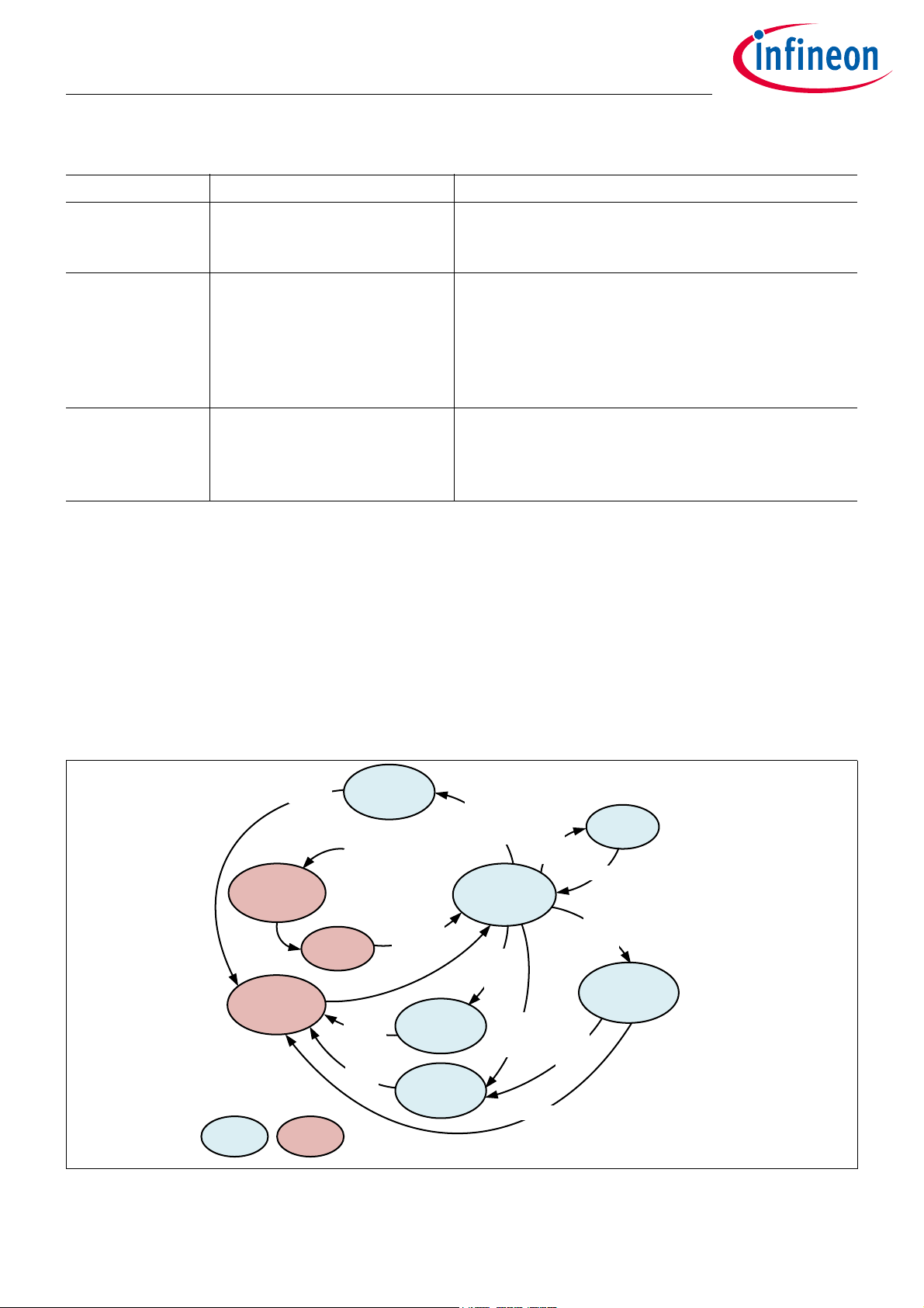
4.3 State Transitions
Figure 2 shows the possible state transitions in normal mode. The central device state is run state because only
in run state the state transitions can be configured. Entering other states from run state is controlled by
application code, either by calling firmware functions [1] or setting control bits [2]. State transitions from other
states are controlled by hardware events, e.g. timer events or LF receiver events.
Figure 2 State transitions in normal mode
Data Sheet 22 Revision 1.2
2020-05-14
Page 23

SP40PLUS
Tire Pressure Monitoring Sensor
Special Features of the SP40PLUS
Table 24 gives an overview of the event sources and the corresponding indicator flags. For each indicator flag
there is an accordant masking flag. However, it does not matter if an event is masked out or not, the indicator flag
will always be set if the event occurs, provided that the indicator register is powered. The masking flag only
determines if the event generates a wake-up/resume. Because not all event sources and all registers are powered
in all power states the actual event indicator flag behavior depends on power state. This behavior is also reported
in Table 24. Furthermore the table shows if the event will generate a resume/wake-up from the respective power
state. Especially in TX low power state certain wake-up/resume events are blocked by hardware in order not to
interrupt a running RF transmission.
(The flag SYSST.TDET, which indicates resume from thermal shutdown, works somewhat differently than the
other wake-up /resume flags. Therefore it is not reported in Table 24 but in Table 25, instead.)
Table 24 Event sources and indicator flags for all device states
Event Event indicator
flag
Power down Deep idle TX low
power
Idle state Run state
indicator flag behavior / event generates wake-up/resume
Interval timer elapsed WUF.ITIM_FLAG raised / yes raised / yes raised / yes raised / yes raised / n.a.
External signal at PP2 WUF.EXT_FLAG raised / yes raised / yes raised / no raised / yes raised / n.a.
LF carrier detected WUF.CD_FLAG raised / yes raised / yes raised / no raised / yes raised / n.a.
LF sync match WUF.SYNC_FLAG raised / yes raised / yes raised / no raised / yes raised / n.a.
LF pattern 0 match WUF.PM0_FLAG raised / yes raised / yes raised / no raised / yes raised / n.a.
LF pattern 1 match WUF.PM1_FLAG raised / yes raised / yes raised / no raised / yes raised / n.a.
LF end of message WUF.EOM_FLAG raised / yes raised / yes raised / no raised / yes raised / n.a.
LF buffer full WUF.BF_FLAG raised / yes raised / yes raised / no raised / yes raised / n.a.
Timer 0 underflow REF.RET0 cleared / no unchanged / no unchanged / no raised / yes raised / n.a.
Timer 1 underflow REF.RET1 cleared / no unchanged / no unchanged / no raised / yes raised / n.a.
1)
/ no
2)
raised / yes raised / n.a.
/ no
raised / yes raised / n.a.
TX encoder buffer empty REF.RERFU cleared / no unchanged / no undefined
TX encoder shift register empty REF.RERFF cleared / no unchanged / no undefined
ADC end of conversion (reserved) cleared / no unchanged / no raised / no raised / yes raised / n.a.
Sampling timer elapsed REF.RESTF cleared / no unchanged / no unchanged / no raised / yes raised / n.a.
Sampling timer power-up (reserved) n.a. / no n.a. / yes n.a. / no n.a. / no n.a / n.a.
1) Bit RERFU is only used for CPU transmission mode. It has no meaning if the transmission controller ist used.
2) Bit RERFF is only used for CPU transmission mode. It has no meaning if the transmission controller ist used.
Complementary to the flags in Table 24 there are four additional flags which indicate from which power state the
device woke-up/resumed. Further there is a flag which is set if any unmasked wake-up event was detected and
another flag which is set if any unmasked resume event was detected. These six flags and their behavior are listed
in Table 25. Figure 4-1 shows how all the flags from Table 24 and Table 25 are connected.
Table 25 Additional wake-up/resume indicator flags
Condition for raising the flag Flag name Power
down
Wake-up from power down
Resume from thermal shutdown
Resume from deep idle
SYSST.WUPDWN raised
SYSST.TDET raised
RESYSCF.REDIDLE raised
Resume from TX low power RESYSCF.RETXLP
A non-masked wake-up event DSR0.WUPEND
raised raised raised raised raised raised
A non-masked resume event DSR1.REPEND
Data Sheet 23 Revision 1.2
2020-05-14
Thermal SDDeep
idle
TX low
power
Idle Run
state
raised
raised raised raised
Page 24

Wake-Up Controller
CD_FLAG
SYNC_FLAG
PM0_FLAG
PM1_FLAG
EOM_FLAG
BF_FLAG
ITIM_FLAG
EXT_FLAG
WUF
CD_MASK
SYNC_MASK
PM0_MASK
PM1_MASK
EOM_MASK
BF_MASK
ITIM_MASK
EXT_MASK
WUM
TDET
SYSST
State-
machine
OR
logic
OR
logic
WUPEND
WUPDWN
DSR0
SYSST
System Controller
RET0
RET1
RERFU
RERFF
reserved
reserved
reserved
RESTF
REF REFM
State-
machine
OR
logic
OR
logic
REPEND
REDIDLE
DSR1
RESYSCF
RET0M
RET1M
RERFUM
RERFFM
reserved
reserved
reserved
RESTFM
reserved
(Sample Timer
power-up trigger)
RETXLP
SP40PLUS
Tire Pressure Monitoring Sensor
Special Features of the SP40PLUS
Figure 4-1 Connection between all wake-up/resume related flags
Data Sheet 24 Revision 1.2
2020-05-14
Page 25

Encoder
Manchester
Biphase
SDPLL
FSK
Modulator
ASK
Modulator
PA
PAOUT
XOSC
XIN
XOUT
RF-Transmitter
8051 Based
MCU
I2C
Controller
Timer 0/1 Watchdog
CRC
Core
FSM
RF-Transmission Controller
DMA
RC OSC
2.2kHz
RC OSC
90kHz
RC OSC
12MHz
Clock Generators
Peripheral Ports / I2C /UART
IO-PORT
PP0/SCL
PP1/SDA
PP2
PP3
ROM
Memories
Flash
RAM
Retention
RAM
SFR
Digital
Baseband
Processor
Carrier
Detector
125kHz
Receiver
LFN
LFP
LF Receiver
FSM
Power
Switch
Controller
System Co ntroller
Clock &
Reset
Controller
ADC Controll er
FSM
Clock &
Reset
Controller
Power
Switch
Controller
LF
ON/OFF
Timer
Interval
Timer
Wake Up Controller
IO-Port
Control
GNDA
Power Supply & Reset Generator
VMIN
TEMP
Detector
PA Voltage
Regulator
VDDPA
VDDREG
VDDBAT
GNDD
Measurement Interface
A
D
Ref Voltage
& Offset
DAC
Bandgap &
PTAT
MUX
RD
V1P
V1M
V1N
V2P
V2M
V2N
VDD
VDD
Data & Address Bus
Sensor Interface
Bond Wire
Surveillance
High Power
Voltage
Regulator
Brown Ou t
Detector
Low Power
Voltage
Regulator
MEMS Sensor
Die
A-Cell
P-Cell
SP40PLUS
Tire Pressure Monitoring Sensor
Functional Descriptions
5 Functional Descriptions
5.1 SP40PLUS Block Diagram
Figure 2 SP40PLUS Block Diagram
5.2 Wake-up Controller
In a typical TPMS application the SP40PLUS is in power-down state most of its operating lifetime. In power-down
state, which is triggered by calling the firmware function Lib_Serv_Low_Power(2), the device is controlled only
by the wake-up controller. The wake-up controller is the block with highest priority in terms of power
management. It is always powered and waits for a wake-up event from different sources. For lowest power
consumption the wake-up controller is clocked by the 2.2 kHz oscillator. If a wake-up event happens and the
event is not masked then the wake-up controller powers on the system controller which takes over device
control. The device wakes up in the same mode (normal- or debug- mode) from which power-down was called.
Before code execution starts the CPU runs a firmware boot sequence and all registers are initialized with their
wake-up values. In case of normal mode the time from wake-up event occurrence until start of application code
execution is in the range of several milliseconds (see Table 20) . The implemented wake-up sources are:
•Interval timer
• LF-Receiver: carrier detector
• LF-Receiver: sync pattern detector
Data Sheet 25 Revision 1.2
2020-05-14
Page 26

SP40PLUS
Tire Pressure Monitoring Sensor
Functional Descriptions
• LF-Receiver: data pattern matching circuit
• LF-Receiver: data buffer full
• LF-Receiver: end of message
• General purpose I/O PP2
• Temperature detector when device is in thermal shutdown
The second main function of the wake-up controller is reset handling. The reset signals themselves are generated
in the block “power supply & reset generator”. A system-reset may be trigged by:
• Brown out (internal regulated voltage drops below a certain threshold)
• Power on
• Under voltage (battery voltage below a certain threshold, see Table 10)
•Software
• Watchdog
• Flash Error (detected via error correction code, ECC)
Apart from the flash error all other system-reset events are not maskable. The register SYSST indicates the reset
source after restart of the device and can be read in application code. After reset release a firmware boot
sequence is executed, the registers are initiated with their reset values, and an I2C handler is called. The handler
waits a certain time (see “mode selection time”, Table 20) for an valid I2C mode selection command [2]. If no
valid I2C signal is received the device starts application code execution after mode selection time elapses.
Although thermal shutdown state is not identical with power-down state, thermal shutdown release event
behaves like a wake-up and all registers are initiated with their wake-up values.
The flag WUPEND allows to distinguish if a wake-up or another restart, i.e. reset or resume, occurred. In case of
thermal shutdown release WUPEND indicates the wake-up, too.
For identification each wake-up source has its own flag in register WUF (only flag TDET is located in SYSST.)
Several flags may be set in WUF if more than one wake-up event occur before reading WUF. Since WUF is cleared
on read, it is recommended not to read single bits but copy WUF into RAM before analyzing it. The flags in the
corresponding WUM register are used for masking individual wake-up sources. Although there is a masking flag
for the interval-timer this flag has no effect: the interval-timer wake-up is not maskable for fail-safe reasons. Note
that if masking a wake-up event in the WUM register the corresponding wake-up is not triggered when the event
occurs, but the corresponding flag in the WUF register is always set, independent of the WUM setting and
independent on device state (low power, run state etc.). This way it is possible to check the WUF for events that
did not trigger a wake-up in order to process these events at a later point in time.
Furthermore the wake-up controller comprises the LF ON-OFF timer that allows operating the LF-receiver with a
configurable duty cycle for power saving reasons. Details see Chapter 5.11.
Important registers associated with the wake-up controller are:
• DSR0 (bit WUPEND. This bit indicates a pending wake-up event)
• SYSST (indicates the system reset source)
• RMASK (Reset mask register)
•WUF (indicates the wake-up source)
• WUM (for masking certain wake-up sources)
• CFG0 (bit SRESET for triggering software reset)
5.2.1 Interval Timer
The purpose of the interval timer is to periodically wake-up the device from power down. The timer is active in
any low power state and is clocked by the 2.2kHz oscillator. The interval timer is counting down, a wake-up event
Data Sheet 26 Revision 1.2
2020-05-14
Page 27

SP40PLUS
Tire Pressure Monitoring Sensor
Functional Descriptions
is triggered upon timer underflow. Although there is a masking bit available in WUM register for the interval timer,
the wake-up event cannot be masked in normal mode. Especially when using the TX-low-power or deep-idle state
it must be made sure by proper timing setting that the interval timer does not interrupt the telegram transmission
or the data acquisition.
The interval timer is separated into a 12 bit pre-counter (SFRs IT0 and IT1) and a 12 bit post-counter (SFRs IT2 and
IT3). For calibrating the pre-counter a firmware function is provided. The post-counter is set by directly writing to
IT2/IT3. This concept allows for quick changing of the timer interval by just changing IT2/3 without running the
calibration routine. Note that writing to IT0/1/2/3 is setting the pre- and post-counter preload value, reading
IT0/1/2/3 provides the current counter reading. The timer is automatically reloaded after underflow.
In thermal shutdown the interval timer is used for periodically checking the temperature detector.
The associated registers are:
• IT0, IT1: interval timer pre-counter (also referred to as tick counter)
• IT2, IT3: interval timer post-counter (also referred to as period counter)
• CFG0.ITINIT: Setting this bit initializes the interval timer with the preload value
5.2.2 LF ON-OFF Timer
The ON-OFF timer is used for switching on and off the LF receiver with a low duty cycle in order to save energy.
Consequently the timer supports long OFF-times of up to 5.7 sec and shorter ON-times of maximal 0.36 sec. Note
that the LF reception is inhibited 3.9 ms by design after being switched on because the LF receiver needs some
time to settle, i.e. the effective On-time is accordingly shorter.
Here are the minimum ON-times for some use cases:
• Carrier Detection for LF-CW signal: minimum ON-time = 3.9 ms + 0.1 ms = 4 ms
• Carrier detection for pulsed LF carrier: minimum ON-time = 3.9 ms + 4.75 ms = 8.7ms
• Data reception mode for periodic repetition of LF-telegram: minimum ON-time = 3.9 ms + period time
The user does not need to directly access the ON-OFF timer registers since the firmware function
Lib_Serv_OnOff_Timer_Calib() can be used for configuration. Setting bits ENLFRX and ENOOTIM activates the
ON-OFF timer. The current count value of the ON-OFF timer cannot be read by software.
Associated registers:
• LFRXC, bits ENTOOM and ENLFRX
5.2.3 LF receiver wake-up/resume events
All wake-up events generated by the LF receiver are maskable. The events are:
• Carrier detected
• Sync pattern detected
• Wake-up pattern match
• Data buffer full detected
• End of message
Refer to Chapter 5.11 for more details.
5.2.4 General purpose I/O PP2 wake-up/resume event
I/O Port PP2 allows maskable wake-up from an external source. In order to use this wake-up source, PP2 needs
to be configured as input (Flag PPD2=1), the corresponding pull resistor must be enabled (Flag PPO2 = 1) and the
corresponding wake-up must be enabled (Flag EXT_MASK = 0).
Data Sheet 27 Revision 1.2
2020-05-14
Page 28

Device
Operable
Device Operable
Device
in Res et
Device
in
Reset
0V
3V
time
V
UVRA
V
THR
VDDBAT
t
MS
t
ini
t
MS
t
ini
SP40PLUS
Tire Pressure Monitoring Sensor
Functional Descriptions
The flag PPS2 is used to define whether the wake-up is triggered on high or low level. If PPS2 = 1 wake-up is
triggered on high level at PP2 pin.
5.2.5 Power-on and under-voltage reset
Figure 3 shows the device behavior depending on voltage at VDDBAT pin. If the voltage falls below a certain
threshold V
reset release threshold V
After the initialization phase the operation mode of the device can be selected by sending an I2C command. The
mode selection is only possible during the time interval t
command, the device goes into normal mode. If a valid I2C command is received during t
in the corresponding mode right after command reception. Table 26 shows the behavior of the device during t
depending on received I2C command.
a system-reset is triggered. The device stays in reset until the voltage at VDDBAT pin exceeds the
UVRA
. After reset release the device initialization is started which takes a certain time, t
THR
. If tMS elapses without reception of any valid I2C
MS
the device starts up
MS
ini
MS
.
Figure 3 Power-on and under-voltage behavior
Table 26 SP40PLUS behavior during mode selection phase
I2C Command Device behavior
None Start with normal mode after t
Wrong I2C address Start with normal mode after t
Invalid mode selection command Start with normal mode after t
Valid mode selection command Start with selected mode immediately after command reception
5.2.6 Software reset, watchdog reset and flash error reset
After a reset triggered by software, watchdog or flash-error the device runs through the reset boot sequence and
the mode selection phase.
The software reset can be triggered by setting the bit SRESET (located in register CFG0) in application code.
A flash-error reset occurs if the flash error correction logic (ECC) detects a non-correctable double bit error (ECC2)
when reading a byte from flash.
Register SYSST is used to identify the reset source after a system reset.
elapsed
MS
elapsed
MS
elapsed
MS
Data Sheet 28 Revision 1.2
2020-05-14
Page 29

SP40PLUS
Tire Pressure Monitoring Sensor
Functional Descriptions
5.2.7 Thermal Shutdown
Thermal shutdown is triggered by calling the firmware function Lib_Serv_Thermal_Shutdown() in application
code. This firmware function brings the SP40PLUS into shutdown if the temperature is either above the hot
temperature threshold T
temperature detector. Once in thermal shutdown the device is only released if the on-chip temperature detector
indicates a temperature below the hot release temperature T
T
. In order to save energy during thermal shutdown the temperature detector is not powered continuously
COLD_RE
but switched on periodically by the interval-timer. The period is defined by function parameter when calling
Lib_Serv_Thermal_Shutdown().
After release from thermal shutdown a wake-up is performed and flag WUPEND is set. However, in this case the
wake-up source is not indicated by WUF register, but by bit SYSST.TDET.
5.3 System Controller
Main function of the system controller is power management after device wake-up from power-down or device
resume from idle, deep idle state or TX-low-power state. Unlike the wake-up controller most other circuits can be
disconnected from power individually. Depending on the device state the system controller connects the
required blocks to the power domain. Here the device states are listed, ordered by current consumption, starting
with the state with highest current consumption:
or below the cold temperature threshold T
HOT_TH
HOT_RE
by using a dedicated
COLD_TH
or above the cold release temperature
• TX low power state during RF transmission
•Run state
• Idle state (run state with CPU disconnected from system clock)
• TX low power state during interframe time
• Deep idle state
• Power-down state (optional with LF receiver enabled)
1)
Important registers associated with the system controller are:
• REF (maskable resume event flag register)
• RESYSCF (indicates resume from deep-idle and TX-low-power)
• REFM (resume event mask register)
• DSR1 (bit REPEND. This bit indicates a pending resume event)
• CLKCFG (field DIVIC for selecting an optional system clock division factor)
1) The power-down state is controlled by the wake-up controller and not by the system controller
Data Sheet 29 Revision 1.2
2020-05-14
Page 30

x Ca librate s ampling ti mer
x Start sampling timer
Idle state
All measurements done?
Deep Idle
no
x Stop sampling timer
Start sampling sequence
Stop sampling sequence
x Call Lib_Acq_Meas_Acceleration()
Resume from idle state
Resume from deep idle state
Resumed from
deep idle?
Idle state
yes
no
CPU start-up period
Resume from idle state
Sampling period
Sampling timer
ADC-trigger event
x S tore measurement value in
Retention RAM
Execute other application code
Code execution started at reset
vecto r
Color code:
Application code
executed
Jump point (label)
No app lication co de
execution
Sampling timer
ADC-trigger event
Sampli ng time r
power-up event
SP40PLUS
Tire Pressure Monitoring Sensor
Functional Descriptions
5.3.1 Sampling Timer
In certain applications periodic acceleration measurements must be carried out over a longer period of time.
There are two major requirements for this application: low power consumption and exact keeping of time
(sampling interval) between two acceleration measurements. In order to meet these requirements a timer is
needed which runs in a device state with very low power consumption, namely the deep idle state. Unlike in
power-down, in deep idle the 90 kHz oscillator is running for providing the needed timing accuracy.
Figure 4 Sampling timer application flow
In order to use the sampling timer it needs to be calibrated and started in application code (see flow diagram in
Figure 4). Subsequently idle state must be entered immediately because resume from idle (ADC triggered event)
occurs only a few 10µs after starting the timer. After resume from idle, when application code execution
continues, the acceleration acquisition function should be called at first. Thereafter additional application code
can be carried out in order to store measurement values in retention RAM.
If more samples must be acquired, application code then enters deep idle state in order to save energy; otherwise
the sampling timer can be stopped and the sequence is terminated. The sampling timer resumes the device from
deep idle state by power-up event. The CPU is re-started and code execution starts from the reset vector. Here
the application code must decide if the device was restarted from deep idle state or not. If yes, idle state is
Data Sheet 30 Revision 1.2
2020-05-14
Page 31

SP40PLUS
Tire Pressure Monitoring Sensor
Functional Descriptions
entered and the next sample is measured when idle state ends. If not, the CPU was restarted due to another event
and the corresponding application code must be executed.
The implementation of the two trigger events allows exact keeping of sampling period because resuming from
idle state occurs without time delay and the idle state period buffers possible variations of the start-up time. In
order to save energy the idle period should be kept as short as possible.
There is no need to configure the sampling timer registers directly because the library function
Lib_Serv_Sample_Timer_Calib() is available for this purpose [1]. The execution time of the application code
marked by the dashed rectangle in Figure 4 is an input parameter for this function. The function calculates the
point of time for resume from deep idle by considering the code run time and the power-up time (the power-up
time is composed of hardware start-up time and firmw are boot sequence, for the exact value see Table 20). This
way the idle period is kept no longer than necessary because power consumption in idle state is higher than in
deep idle state.
Note that the deep idle state can be terminated by LF-receiver events , interval-timer or PP2 event. Hence it must
be made sure in application that sampling phase is not affected by one of these event sources, e.g. by masking
the corresponding flags.
Associated registers:
•STIMCFG0 (sampling timer low byte)
• STIMCFG1 (bit EN for enabling sampling timer and sampling timer high bits)
• STIMCFG2 (power up period configuration)
5.4 Clock Generators
The SP40PLUS comprises three on-chip RC oscillators in order to fulfill the extremely different requirements in
terms of power consumption and cycle time for different operating states. A 2.2 kHz oscillator is operated in
power-down for lowest power consumption. A 90 kHz oscillator is implemented for clocking the system
controller, the interframe timer, the sampling timer, and the digital part of th e LF receiver. Finally a 12 MHz
oscillator is used for the CPU. This clock may be divided (controlled by bit field DIVIC) and is called system clock.
The 90 kHz and 12 MHz clock sources are switched on by the wake-up controller and the system controller,
respectively, and only if needed. The 90 kHz and 12 MHz oscillators are trimmed in production.
For RF transmission and calibration purposes a crystal oscillator is implemented as well. Details about the
implementation of the crystal oscillator are described in Chapter 5.9.7.
Figure 5 shows a fundamental clock distribution diagram, i.e. which clock source is used for which digital block.
The white triangles (gates) indicate for which blocks the clock can be gated in order to save energy. For most
blocks the gating is done automatically. In some cases gating can be controlled by application code. In this case
the corresponding control bit is drawn next to the gate.
Most SFRs are always clocked by system clock if the CPU is running. But there are some exceptions which are
depicted in Figure 5, namely registers RFD, RFS and RFENC. Clock distribution to these registers is controlled by
internal control bits TXMASTER and RFENC. These control bits are configured by firmware function
Lib_Serv_Config_RF_Transmission. The bits are mentioned for information only.
Data Sheet 31 Revision 1.2
2020-05-14
Page 32

RC OSC
2.2kHz
RC OSC
90kHz
Wake-Up
Controller
FSM
Timer 0/1
Watchdog
LF-Digital
Baseband
LF
ON/OFF
Timer
ENOOTIM
Sampling
Timer
System
Controller
FSM
Interframe
Timer
EN
RC OSC
12Mhz
I2CMEIF UART
I2CEN
Divider
CRC
Interval
Timer
UARTEN
TIMEN
XOSC
26MHz
DIVIC
Encoder
Manchester
Biphase
RF
Transmitter
FSM
PLL
RFD
RFENC.RFDLEN
RFENC.RFMODE
0 1
TXMASTER
1)
TXDEN
1)
CPU
OBW
Controller
OBWCE N
RFS
1) Internal registers, see text
SP40PLUS
Tire Pressure Monitoring Sensor
Functional Descriptions
Figure 5 Clock distribution diagram
5.5 Core
The Core comprises a 8051 based MCU and the following peripherals:
•Timer Module
•Watchdog
• Hardware CRC
•I2C Controller
•UART interface
Data Sheet 32 Revision 1.2
2020-05-14
Page 33

SP40PLUS
Tire Pressure Monitoring Sensor
Functional Descriptions
5.5.1 Timer Module
The timer module consists of six registers TCON, TMOD, TL0, TH0, TL1 and TH1. The timer module enable bit
TIMEN is located in register CFG2. Those firmware routines that are using timers disable the timer module prior
to returning to application code. Therefore generally TIMEN should be set before timer module is configured and
started in application code. TIMEM should be cleared if the timers are no longer used in order to reduce power
consumption.
The timer module can be configured to 8 different modes (mode 0 to 7) by setting the three TM bits accordingly.
The modes differ in timer length (8 bit or 16 bit) and timer behavior (timer stops on underflow or timer reloads
and restarts on underflow). The four registers are either used as down counter or for holding the reload value. In
principle following timer modes are supported:
• Two 16 bit timers without reload (single run)
• Two 8 bit timers with reload
• One 16 bit timer with reload
• One 16 bit timer without reload plus one 8 bit with reload
• Three 8 bit timers, one with reload.
Table 27 and Table 28 show in detail how the registers are configured in each mode. Timer mode 7 is not
reported because this mode is not available in application code, but is used by firmware for calibration purposes.
The timer module does not allow CPU interrupt. Instead of that the timer underflow bits need to be polled in
application code. The timer module can be clocked from different clock sources thus providing a wide range of
timing cycles and allowing for calibrating internal clock sources with the crystal oscillator. The clock source for
timer 0/1 depends on the clock source select bits T0CLK and T1CLK and on the timer module crystal clock enable
bit TCLKM. Following clock sources are selectable:
• 12 MHz RC oscillator divided by 1, 8, 32, 128 or 512 (independent from DIVIC)
• 4.4 kHz, derived from 2.2 kHz low power RC oscillator
• Timer 0 only: clocked by timer 1 underflow
• Timer 1 only: rising edge at PP2
• Crystal clock divided by 6
• Timer 0 only: Crystal clock divided by 512
• Timer 0 only: 90 kHz RC divided by 8
Note: the timer clock source must not be mixed up with the system clock used for loading the timer registers. The
timer module system clock is always 12MHz with a division factor defined by DIVIC (see Figure 5).
Timer configured without reload
If a timer is configured to work without reload it stops on underflow and must be restarted by software. Prior to
starting the timer it can be loaded with an initial value. When started by setting the timer run bit the timer counts
down from the initial value to zero. When the timer has reached zero the underflow event is triggered on the next
clock cycle. The timer run bit is cleared on underflow; the timer full flag is set on underflow.
Timer configured with reload
If a timer is configured to operate with reload it is automatically reloaded from a reload register and restarted on
underflow. Prior to starting the timer it can be loaded with an initial value different from the reload value. A timer
full flag indicates underflow and must be cleared by software. The timer is started by setting a timer run bit and
stopped by clearing this bit.
Data Sheet 33 Revision 1.2
2020-05-14
Page 34

SP40PLUS
Tire Pressure Monitoring Sensor
Functional Descriptions
Table 27 Timer Modes 0 to 2
Register or
Flag Name
TL0 timer 0: 16 bit timer with
TH0 timer 0 reload value
TL1 timer 0 reload value timer 1: 8 bit timer with reload timer 1: 8 bit timer with reload
TH1 timer 1 reload value timer 1 reload value
T0RUN timer 0 run bit timer 0 run bit timer 0 run bit
T0FULL timer 0 full bit timer 0 full bit timer 0 full bit
T1RUN not used timer 1 run bit timer 1 run bit
T1FULL not used timer 1 full bit timer 1 full bit
Table 28 Timer Modes 3 to 6
Mode 3 Mode 4 Mode 5 Mode 6
timer 0.1: 8 bit timer w/o
reload
timer 0.2: 8 bit timer w/o
reload
timer 1: 8 bit timer with reload timer 1: 16 bit timer
timer 1 reload value
Mode 0 Mode 1 Mode 2
reload
timer 0: 16 bit timer without
reload
timer 1 reload value timer 0: 8 bit timer with
reload
timer 0 reload value
timer 1: 16 bit timer without
with reload
reload
timer 0: 8 bit timer with reload
timer 0: 16 bit timer without
reload
timer 1: 16 bit timer without
reload
timer 0.1 run bit not used timer 0 run bit timer 0 run bit
timer 0.1 full flag not used timer 0 full flag timer 0 full flag
timer 0.2 run bit timer 1 run bit timer 1 run bit timer 1 run bit
timer 0.2 full flag timer 1 full flag timer 1 full flag timer 1 full flag
Note that in timer modes 1, 2 and 3 timer 1 is used as Baud-rate generator for RF transmission. Hence, for RF
transmission, the timer module must be configured to one of the three mentioned modes.
With timer module associated registers:
•TCON
•TH0
•TH1
•TL0
•TL1
•TMOD
•CFG2 (bit TIMEN)
5.5.2 Watchdog
The watchdog timer is clocked by the 2.2 kHz oscillator. It is active in all run states and in idle state and cannot be
disabled. The nominal time-out occurs after 2048/2.2 kHz ~ 1sec. In order to avoid a watchdog reset event the
watchdog timer must be reset in application code by setting the flag WDRES periodically. In all low power states,
except from idle state, the watchdog timer is disabled and has no effect. On wake-up or resume from a low power
state, except from idle state, the watchdog is reset automatically.
Data Sheet 34 Revision 1.2
2020-05-14
Page 35

SP40PLUS
Tire Pressure Monitoring Sensor
Functional Descriptions
In program- and debug-mode where the device is controlled by I2C the firmware I2C handler resets the watchdog.
Since in idle state no application code can be executed, idle state must not take longer than the watchdog timeout period.
Associated register:
•CFG2 (bit WDRES for resetting watchdog)
5.5.3 Hardware CRC
The SP40PLUS comes with a hardware CRC module. This module calculates a 16 bit CRC value of an arbitrary
sequence of bytes in accordance with the CRC-CCITT (CRC16) standard, i.e. using the polynomial 0x1021. As start
value for CRC calculation 0xFFFF should be used, however the CRC module may be initialized with other start
values as well.
The CRC module is used by the firmware I2C handler which checks the CRC value of incoming I2C commands and
calculates the CRC value for outgoing telegrams.
CRC of a sequence of data bytes
The CRC module can be used in application code as well. For this end the start value 0xFF must be loaded into the
two CRC registers CRC1 and CRC0, respectively. Then the data bytes are written subsequently into the CRC data
register CRCD. After processing all data bytes registers CRC1 and CRC0 hold the result.
The flag CRCVALID is set automatically if the result is zero, i.e. CRC1 and CRC0 are both zero. This flag can be used
for simply checking the CRC of incoming telegrams by initializing CRC1 and CRC0 with 0xFF, then subsequently
writing the data bytes and the two CRC bytes of the telegram to the CRC data register. If there is no bit error in the
telegram the result is zero and CRCVALID is set.
CRC of a serial bit-stream
The CRC hardware can also be used for calculation of the CRC of a serial bit-stream. The bit CRCSD is the input for
the serial bit-stream. The bit CRCSS is the corresponding strobe signal.
As for byte processing the result registers CRC1 and CRC0 must be initialized with 0xFF, respectively. After writing
a bit into CRCSD, bit CRCSS has to be set and reset by software. Then the next bit is written into CRCSD and so on.
If a bit-stream is longer than 8 bit, serial and byte-wise CRC encoding can be mixed. As long as more than 8 bits
are left, data can be written byte-wise into the CRC data register. Finally, the residual bits are processed using
CRCSD and CRCSS.
With hardware CRC associated registers:
• CRCC (bits CRCSD, CRCSS, CRCVALID)
•CRCD
•CRC0
•CRC1
5.5.4 I²C Controller
The SP40PLUS features a slave hardware I2C interface with the fixed device address 0x6C. When the I2C is
activated, pin PP0 is configured as input and serves as clock line (SCL). Pin PP1 is initialized as input, too, and
serves as data line (SDA). Both lines need a pull-up resistor, either an external resistor or by activating the internal
pull-up resistors. The active device transmits data by pulling the data line low.
In program- and debug- mode the I2C interface is managed by a firmware I2C handler. Only certain I2C commands
are available in these modes, no application code can be executed. The internal pull-up resistors are enabled by
the I2C handler.
Data Sheet 35 Revision 1.2
2020-05-14
Page 36

n repetitions for n data bytes
01 67
R/WA6A7 A1
8
D7ACK D6
01
78
ACKD0
address R/W=0 A=0 data A=0 stopstart
address A=0 data A=0 stopstart
CLK
SDA
Data read
n-1 repetitions
067
R/WA7 A1
8
D7
ACK
0 78
ACKD0
CLK
SDA
R/W=1
D7
0 78
ACKD0
Data write
data n A=1
SP40PLUS
Tire Pressure Monitoring Sensor
Functional Descriptions
In power-down state the I2C is disabled and PP0 and PP1 stay in the state configured by application code. In
program- or debug- mode is not possible to switch the SP40PLUS into power-down by I2C command.
In normal mode the I2C (if needed) must be managed by application code. For activating the I2C interface the bit
I2CEN must be set. If internal pull-up resistors shall be used the bits PPI0 and PPO0 must be set in order to enable
the pull-up resistors of pin PP0. Bits PPI1 and PPO1 must be set in order to enable the pull-up resistor of pin PP1.
The port direction register is managed automatically by the I2C interface.
Receiving data from master in normal mode
Once activated, the I2C register waits for a start condition. The following 8 bits are interpreted as device address
and compared to 0x6C. If the received address matches, acknowledge (ACK) is generated, i.e. the data line is
pulled down on the 9th clock pulse. The address match is indicated by the flag AM. Polling this flag may be used
to branch into a data reception subroutine.
The next 8 bits are interpreted as data bits and are also acknowledged by pulling the data line low. The complete
reception of a data byte is indicated by the flag I2C_RBF. The application code needs to poll this flag and fetch the
data from the register I2CD. I2C_RBF is cleared automatically when reading I2CD. This procedure is repeated for
incoming data bytes until a stop condition is received. The flag I2C_S indicates that a stop condition has been
received.
Transmitting data from SP40PLUS to master in normal mode
The LSB of the device address serves as a read-write indicator. Thus, in order to put the SP40PLUS in data
transmission mode, the master must send the device address 0x6D. The flag I2C_RNW indicates to the software
that the read-write indicator bit is set and that data can be transmitted from SP40PLUS to the master. The
software can poll this flag for branching into a data transmission subroutine. In this subroutine data bytes can be
written into the I2CD register when the flag I2C_TBF does not indicate a full transmit buffer. This procedure can
be repeated for outgoing data bytes until a stop condition is received.
The I2C interface also provides a data overflow flag. This flag is set if new data is received before reading I2CD or
data is written to I2CD before transferring the previous data byte to the I2C shift register.
The principle I2C data transfer is shown in Figure 6. The shaded areas indicate when SDA line is controlled by the
master, the non-shaded areas when the SDA line is controlled by the sensor.
Figure 6 Data transfer on the I2C bus
Data Sheet 36 Revision 1.2
2020-05-14
Page 37

SP40PLUS
Tire Pressure Monitoring Sensor
Functional Descriptions
With the I2C controller associated register:
•CFG2 (bits I2CEN and I2CGCEN)
•I2CD
•I2CS
5.5.5 UART Interface
The SP40PLUS has a hardware UART interface. If enabled, pin PP2 serves as UART-RX and PP3 as UART-TX. (Note
that the port direction, i.e. PP2 as input and PP3 as output, must be configured in application code. Note also that
setting Bit CFG2.UARTEN automatically disables any pulling-resistor at PP2.) The UART port is half-duplex, i.e.
data transmission and reception must not occur simultaneously. The port is receive buffered, i.e. a second byte
can be received before the previous byte is read from the receive register.
Although there are separate shift registers for reception and transmission, both registers are accessed via the
same special function register UASBUF. Reading UASBUF accesses the receive buffer and writing to UASBUF
accesses the transmission shift register.
The UART interface supports an 8 bit data mode with 1 stop bit which is added automatically. The transmission
is activated by a write operation to UASBUF. End of byte transmission is indicated by flag TI. This flag must be
cleared by software. The receive flag RI indicates that a byte can be read from the receive buffer. This flag must
be cleared by software, too.
The UART interface has a Baud-rate generator which is clocked by the system clock, i.e. by the 12 MHz oscillator.
The Baud-rate generator consists of a prescaler, a timer and a fractional divider. The prescaler divides system
cl ock, t he d ivisi on f actor is s elect ed b y a three b it v alue BRPR E. T he tim er i s coun tin g downwar ds; it is loaded w ith
the value BR_VALUE on underflow. The fractional divider provides an output clock that is given by the input clock
divided by 256 and multiplied by the 8 bit value UASFDSTEP.
Table 29 shows possible Baud rates and the corresponding register settings.
Table 29 UART Baud-rate selection
Baud-rate BRPRE BR_VALUE UASFDSTEP
19200 000
28800 000
38400 000
56000 000
57600 001
115200 000
B
B
B
B
B
B
35 236
23 236
17 236
8 172
5 236
5 236
Following registers are associated with the UART interface:
• UASCFG (bits RCLKEN and TCLKEN for enabling the receive and transmit clock)
• UASCON (indicator flags RI and TI and receiver enable bit REN)
• UASBUF (for accessing receive buffer and transmit shift register)
• UASBCON (containing the Baud-rate generator enable bit R and the prescaler control bits BRPRE)
• UASBG (containing the Baud-rate timer reload value BR_VALUE)
• UASFDCON (with the fractional divider enabling bit FDEN)
• UASFDSTEP (containing the fractional divider configuration value UASFDSTEP)
• UASFDRES (serial port fractional divider result register)
•CFG2 (bit UARTEN)
Data Sheet 37 Revision 1.2
2020-05-14
Page 38

1kB
40k B
12k B
25 6
Bytes
16 0
Bytes
0xF3FF
0xEFFF
0xB3FF
0xEFFE
0xC000
0xB3FE
0xB000
0x9FFF
0x00 00
0xF300
0xFF FF
0xFF60
IFX Configurat ion
Sector
Firm ware
Code Sector
User Configuration
Sector
Retentio n RAM
Lockbyte 1
Lockbyte 2
Lockbyte 3
Flash
RO M
RAM
legend:
0xF3FE
SP40PLUS
Tire Pressure Monitoring Sensor
Functional Descriptions
5.6 Memories
The 8051 based microcontroller core is able to address a 64kB wide range of code memory. In the SP40PLUS this
address range is used for the following types of memory:
• 40 kB ROM for firmware
• 1 kB Flash memory for factory configuration data (IFX configuration sector)
• 12 kB Flash memory for application code (user code sector)
• 256 byte Flash memory for user configuration data (user configuration sector)
• 5x32 byte Retention RAM
Figure 7 shows the corresponding memory mapping. The content of the ROM sector and IFX configuration sector
cannot be changed. Both sectors are protected against reading by lock-byte 1, which is factory set.
Each flash byte is secured by a five bit error correction code (ECC). The ECC bits are generated automatically when
the flash byte is programmed. When a flash byte is read, the error correction unit can correct all single bit errors
and detect all double bit errors.
Figure 7 Code memory organization
5.6.1 Lock-byte concept overview
At the end of each flash sector there is a lock-byte, which may be enabled by the user in order to protect the sector
against overwriting and reading. In order to activate a lock-byte it must be written with the value 0x69. However,
for security reasons, other lock-byte values with a Hamming distance from 0x69 of up to 3 are also considered as
valid. The two lock-bytes are not independent from each other: lock-byte 2 has a higher priority than lock-byte 3,
i.e. lock-byte 3 can only become effective if lock-byte 2 is already enabled.
Furthermore enabling lock-bytes only becomes effective after device reset.
Data Sheet 38 Revision 1.2
2020-05-14
Page 39

User Cod e User Config
Read: yes
*
Write: no
Erase: yes
Read: yes
*
Write: yes
Erase: yes
Read: yes
*
Write: yes
Erase: yes
Read: yes
*
Write: yes
Erase: yes
Read: yes
*
Write: no
Erase: yes
Read: yes
*
Write: no
Erase: yes
Read: yes
Write: yes
Erase: yes
Read: yes
Write: yes
Erase: yes
Read: yes
Write: yes
Erase all sectors at once: yes
Read: no
Write: no
Erase all sectors at once: yes
Read: no
Write: no
Read: no
Write: no
User Code User Config
Normal Mode Programming Mode
User Code
User Code + User
Config
0x69 0x00
0x69 0x69
Protected Flash
Sectors
LB2 LB3
none 0x00 0x00
*
no firmware support, read flash by using CPU commands MOVX or MOVC
SP40PLUS
Tire Pressure Monitoring Sensor
Functional Descriptions
Figure 8 shows the possible lock-byte settings and their effect on the flash sectors for program mode and normal
mode. Debug-mode cannot be used if lock-byte 2 is active.
Figure 8 Lock-byte settings and effects in program- and normal- mode
5.6.2 Flash programming
For programming the user code sector or the user configuration sector in program mode there are two I2C
commands available. The command Erase-Sectors for deleting the sectors as a whole and the command FlashWrite-Line for programming a 32 byte long flash line. For enabling the lock-bytes LB2 or LB3 the value of the lockbyte location must be defined as 0x69 when writing to the corresponding line with the Flash-Write-Line
command. If a lock-byte shall remain disabled, its value must be defined as 0x00. The I2C command Set-User-
Config-Sector-Lock also allows enabling LB3 after writing the last line. There is no such I2C command for LB2.
For programming the user configuration sector in normal mode, i.e. during runtime, the firmware functions
Lib_Fl_Erase_User_Config_Sector, Lib_Fl_Write_Line and Lib_Fl_Change_UCS_Line() are available. For setting
the user configuration lock-byte (LB 3) the value of the last byte must be defined as 0x69 when writing or changing
the last line of the user configuration sector.
Note: IFX recommends shutting off the flash using I2C command PM Flash Shut Down before disconnecting the
device from supply voltage.
5.6.3 Retention RAM
In order to save information when the device is in a low power state or in thermal shutdown there are 5 blocks of
32 bytes of retention RAM available. Via five configuration bits (RETMEM) each retention RAM block can be
enabled individually for staying always powered. The retention RAM is mapped to the external RAM address
space of the 8051 controller. Hence, in a C environment, the directive XDATA must be used to define a variable
located in retention RAM area.
The retention RAM has random values after power-on, i.e. after being connected to a battery. Enabled retention
RAM will keep its values in all device states as long as the device is connected to the battery.
Associated registers:
• MEMCFG, bits RETMEM
5.6.4 Data RAM and SFRs
The SP40PLUS microcontroller core has a 256 Byte address space for data RAM that can be used in application
code. The address space 0x80 to 0xFF of the upper 128 Bytes of data RAM is shared with the Special Function
Data Sheet 39 Revision 1.2
2020-05-14
Page 40

SFRs (page 2)
SFRs (page 1)
128
By tes
0xFF
0x80
Data
(only indirectly
addressable)
128
By tes
0x7F
0x00
Data
(directly or ind irectly
addressable)
3 x 128
Bytes
SRFs (page 0)
(only directly
addressable)
SP40PLUS
Tire Pressure Monitoring Sensor
Functional Descriptions
Register (SFR) bank. The two register banks are selected via addressing method. If direct addressing is used a SFR
is selected, if indirect addressing is used data RAM is selected. The RAM in the lower addressing range can be
accessed either by direct or indirect addressing. This is illustrated in Figure 9.
The SFR bank consists of three pages. There are two control bits, PAGING0 and PAGING1, for switching between
the three pages. These bits are located in the special function register CPUSYS which is mapped to all pages.
Figure 9 RAM organization
There are some restrictions in using the data RAM. Firmware library functions use certain RAM locations for
internal operations (see ROM Library Guide). Furthermore the upper 128 byte of RAM are used exclusively by the
transmission state machine during RF transmission. Unlike the retention RAM, the data RAM is not powered in
power-down state and deep-idle state. The lower RAM bank is not powered in TX-low-power state.
Memory mapped RAM
There are 3 additional bytes of RAM which are mapped to the code memory range. These bytes are not belonging
to the retention RAM area. Address of the first byte is 0xAFF8. The three RAM locations are intended for executing
a user defined OpCode in order to address SFR indirectly, for instance. See [2] for details.
Associated registers:
• CPUSYS (PAGING0/1 for SFR bank switching)
• MMR0/1/2 (Memory Mapped Registers for execution of runtime programmable OpCode)
5.6.5 Retention SFRs
Many of the SFRs are implemented as retention registers, i.e. they are keeping their values in low power states
like retention RAM. However, other than retention RAM they are all initialized by firmware after a system reset.
Some internal retention SFRs are loaded with values from the Infineon config sector. They are refreshed after
each device wake-up or resume as well.
5.7 Power Supply and Reset Generator
The Power Supply and Reset Generator provides the voltage for different voltage domains:
•Analog domain
• Digital domain
• Voltage domain for retention RAM and SFRs
• Regulated voltage for RF power amplifier
Furthermore this functional block provides a reset signal on power-on and under-voltage for the wake-up
controller (see Chapter 5.2.5).
Note: an external capacitor must be connected to VDDREG-pin in order to stabilize the internal voltage. This pin
must not be used as voltage supply for external devices.
Data Sheet 40 Revision 1.2
2020-05-14
Page 41

SP40PLUS
Tire Pressure Monitoring Sensor
Functional Descriptions
5.7.1 TX battery voltage detector
Part of the power supply block is the TX battery voltage detector. This detector monitors the battery voltage
during RF transmission, i.e. when a frame is transmitted, but not during interframe delay. The detector is
activated automatically by the transmission controller. If battery voltage drops below V
flag BATTXOK is immediately set without time delay (apart from the analog signal propagation delay which is in
the µs range). The bit may be checked by application code after resuming run state.
Associated register:
• DSR1 (bit BATTXOK)
5.8 Measurement Interface
The measurement interface block is the interface between the analog sensor signals and the digital signal
conditioning domain of the SP40PLUS. A multiplexer selects one of the following input signals for the 13 bit
analog to digital converter:
• Pressure Sensor (located on separate MEMS chip)
(see Table 10) then
MIN
• Accelerometer (located on separate MEMS chip)
• Temperature Sensor
• Battery Voltage Sensor
This block also includes a bond wire surveillance circuit which checks the integrity of the connections to the
MEMS chip after each measurement.
5.9 RF transmitter
Figure 10 shows a block diagram of the RF transmitter with associated SFRs. The transmission may be either
controlled by the CPU (CPU mode) or by the transmission controller (TX-FSM). Some registers and bits only need
to be accessed in CPU mode. They are marked with * in Figure 10. The CPU mode is only implemented for the
sake of compatibility with prior products. Since the CPU clock can cause spurs in the transmitted spectrum, in
CPU mode transmission should only take place when the CPU is in idle state. Otherwise RF standards like ETSI
and FCC may not be met. See chapter “User instructions” in the User Manual how to use CPU mode. This following
description focuses on transmission using the transmission controller.
The RF transmitter receives data from the RF transmission controller via the data register RFD (in CPU mode RFD
is directly loaded by application code for single byte transmission). As soon as a data byte is loaded into RFD, the
RF power amplifier is activated and the Manchester/biphase encoder starts encoding. For carrier frequency
generation the RF transmitter has a PLL circuit and a crystal oscillator operated with a 26 MHz standard quartz.
The PLL is a Sigma-Delta (SD) fractional-N type which allows frequency modulation (FSK) by directly changing the
PLL frequency. The transmitter also allows amplitude modulation (ASK) by modulating the VDDPA voltage.
The transmitter supports the 315MHz and the 434MHz band. Part of the PLL is a VCO whose frequency depends
on selected frequency-band, carrier frequency and temperature. Hence the VCO must be tuned prior to
transmission. For this purpose the firmware function Lib_Serv_VCO_Tuning is available. The frequency band is
selected via input parameter of Lib_Serv_VCO_Tuning and the carrier frequency registers must be set before
calling this function.
Data Sheet 41 Revision 1.2
2020-05-14
Page 42

VCO
Fixed divider
XTAL
oscillator
Program mable
divider
Phase
detector
Pre.Ampl.
Power
Ampl.
SD
Modu lator
Gauss
Filter
RFRGCFG0
Transmission Controller
RAM
RFSDCFFRAC0/1/2
RFSDCFINT
RFSDFDCFG
RFSDGFDIV0/1
RFC
RFTXBRDIV0/1
Ext ernal
matching
circuit
PA
VDDPA
VREFRFCTRL
CFG1.T XPDEOTR
RFSDCTRL
RFTXCFG0 RFTXNBITS0/1
RFTXCFG1
RFTXCFG2
RFTXEOM
RFTXSOM /2 /3
RFD
*
RFENC
FSK
ASK
RFS
RFS.RFBF
*
RFS.RFSE
*
Encoder &
Baud rate
generator
ASK ramping
generator and
control
DAC
VDDBAT
RFTXOBW_CFG0
RFTXOBW_CFG1
RFTXOBW_MLV
RFTXOBW_SLV
VREGRFCTRL.BYPASS_REG
1
PLLCFG0
Voltage
regulator
reg.
voltage
SP40PLUS
Tire Pressure Monitoring Sensor
Functional Descriptions
Figure 10 RF Transmitter block diagram
5.9.1 Manchester/Biphase Encoder
The Manchester/Biphase encoder automatically encodes data bytes to a Manchester or Biphase bit-stream
beginning with the MSB. Encoding starts when a byte is loaded into the encoder TX data register (RFD). Also, if the
bit ENPA is cleared, the encoder automatically switches on the RF power amplifier when the encoded data is
shifted out. The encoder needs a clock signal which is provided by the Baud-rate generator, see Chapter 5.9.8.
The encoder can be either used directly in application code by feeding data to RFD or indirectly by using the
transmission controller. In this second case the RF data must be stored in a dedicated RAM location and the
transmission controller manages the transfer of the RF data to the RFD register. Details see Chapter 5.10.
There are several control bits that determine how the data is treated by the encoder. The three bits RFMODE
determine the encoding scheme:
•Manchester
• Inverted Manchester
• Differential Manchester
•Biphase 0
•Biphase 1
• Chip Mode (NRZ)
Chip Mode means that the data bits are not encoded, but sent directly to the modulator. This feature allows user
defined encoding schemes, preambles and intended code violations. Note that in chip mode the bit time is only
half time as in the other modes. Therefore the transmission of one byte in chip mode is completed already after
4 clock cycles. An example of the encoder output signal for the different modes is shown in Figure 11.
Data Sheet 42 Revision 1.2
2020-05-14
Page 43

RFD
Clock
Manchester
Biphase-1
Biphase-0
Differential Manchester
10100110
Inverted Manchester
Encoder Input:
Encoder Output:
Chip Mode
Encoder Input:
Encoder Output:
RFD
1010011
0
Clock
SP40PLUS
Tire Pressure Monitoring Sensor
Functional Descriptions
Figure 11 RF encoding schemes
The bit TXDD determines the output of the encoder before or after transmission. This bit only applies when ENPA
is set, otherwise the RF power amplifier is automatically deactivated after transmission and the encoder output
is meaningless. If the bit ITXD is set the encoder output is inverted. Finally, the 3 bits RFDLEN determine the
number of bits of the RFD data byte to be transmitted beginning with the MSB. Default setting for RFDLEN is 7
meaning that all 8 bits are transmitted.
The encoder unit provides two status bits. The bit RFBF indicates that RFD is full. If this flag is set no data must be
written to RFD. The bit RFSE indicates that all bits have been transmitted.
The encoder supports a monitoring function that automatically disables the RF power amplifier during
transmission if the PLL goes out of lock (indicated by flag OOL) or the crystal oscillator is unstable (indicated by
XFAIL). This function avoids out of band transmission. The status bit PADIS is set automatically if the RF amplifier
is disabled either by PLL or XTAL fail. Note that these monitoring functions are disabled by default and should be
enabled by setting bits ENPLLMON and XOSCPLLMON in order to avoid out-of-band emission.
Special function registers associated with the encoder are:
•RFD
• RFENC (fields RFMODE and RFDLEN, bits TXDD and ITXD)
• RFS (bits RFBF, RFSE, PADIS)
• RFC (bits ENPLLMON, XOSCPLLMON and ENPA)
5.9.2 SD-PLL
For generation of the RF frequency the SP40PLUS comes with a fractional-N Sigma-Delta-PLL (SD-PLL). A
conventional PLL circuit has a divider with a fixed ratio for dividing down the output frequency in order to make
it exactly the same as the reference frequency. In contrary to that, a fractional-N SD-PLL has a divider with a
certain range of divider ratios. The selection of the divider ratio is carried out by a sigma delta modulator. The
Data Sheet 43 Revision 1.2
2020-05-14
Page 44

SP40PLUS
Tire Pressure Monitoring Sensor
Functional Descriptions
sigma delta modulator provides a data stream where each data word means a certain divider ratio. Due to the
integrative behavior of the PLL loop the output frequency becomes the reference frequency multiplied with the
average divider ratio determined by the SD data stream.
The advantage of this method is that the output frequency can be adjusted with a very high resolution.
Furthermore the ratio of output and reference frequency does not need to be an integer value. Hence it is possible
to use the same crystal for different frequency bands, namely the 315 band and the 434 MHz band.
The SP40PLUS allows setting the RF center frequency with a 12 Hz resolution. An eight bit value PLLINT[7:0] is
used for determining the integer part of the frequency and a 21 bit value PLLFRAC[20:0] for the fractional part
according to Equation (5.1).
(5.1)
Registers used for frequency setting are:
• RFSDCFINT (PLLINT)
• RFSDCFFRAC0 (PLLFRAC)
• RFSDCFFRAC1 (PLLFRAC)
• RFSDCFFRAC2 (PLLFRAC)
Other registers:
• RFS (Status bits OOL , XFAIL and PADIS)
• RFC (bits XOSCPLLMON and ENPLLMON)
5.9.3 FSK Modulator
The FSK modulator is part of the SD-PLL. The SD modulator generates a data stream that corresponds to the FSK
low frequency if the FSK data line is low and a data stream that corresponds to the FSK high frequency if the data
line is high. FSK high frequency and FSK low frequency are determined by an 8 bit value FDEV according to
Equation (5.2).
(5.2)
Related register:
• RFSDFDCFG (FDEV)
5.9.4 Gaussian filter
In order to reduce the occupied bandwidth (OBW) in case of FSK-modulation a Gaussian filter for mitigating the
steps between the two FSK-frequencies is implemented. The Gaussian filter is enabled by choosing GFSK option
when calling Lib_Serv_Config_RF_Transmission. The filter effect decreases with increasing filter oversampling
rate in relation to signal chip-rate. The sample-rate is determined by the 12 bit value GFDIV. A good compromise
between modulation shaping and RF sensitivity loss is an oversampling rate of 16. Equation (5.3) provides the
Data Sheet 44 Revision 1.2
2020-05-14
Page 45

SP40PLUS
Tire Pressure Monitoring Sensor
Functional Descriptions
value of GFDIV for a fixed oversampling rate of 16 and a given value of BRDIV. For the relation between BRDIV and
Baud-rate / chip-rate see Chapter 5.9.8.
(5.3)
Associated registers are:
• RFSDGFDIV0 (GFDIV)
• RFSDGFDIV1 (GFDIV)
5.9.5 RF Power Amplifier
The power amplifier is intended to be operated as class-E amplifier which has a higher efficiency than class C
operation. The operation mode is mainly determined by the matching network. (See Chapter 6 for a matching
network proposal.) In order to provide a constant RF output power independent from battery voltage, a voltage
regulator for the RF amplifier is implemented. The voltage is available at VDDPA pin. However, by setting bit
BYPASS_REG, it is still possible to operate the transmitter with unregulated battery voltage.
If the transmission controller is used (FSM mode, Chapter 5.10) then the RF power amplifier (PA) is automatically
switched on and off for transmission. If the transmission is controlled by application code (CPU mode) then the
power amplifier needs to be controlled by switching bit ENPA (see User Manual, chapter User Instructions).
For the sake of low occupied bandwidth the RF power should not be instantly switched, but ramped. In case of
ASK modulation the voltage at VDDPA pin is ramped for this purpose, see Chapter 5.9.6. In case of FSK
modulation a different power shaping mechanism is used. Here the impedance of the PA is ramped. Ramping
time for PA power on and off for FSK is controlled by bitfield RTIME.
1)
Important registers associated with the PA are:
•RFC (bit ENPA, only for CPU mode)
• VREFRFCTRL (supply voltage for PA pin)
•VREGRFCTRL.BYPASS_REG (enables battery voltage at VDDPA)
• RFRGCFG0 (RTIME, only for FSK modulation)
Attention: In order to prevent electrical overstress of the PA stages the transmitter supply voltage must always
be taken from VDDPA pin. It is not allowed to directly connect the transmitter to an external voltage
(=battery voltage).
5.9.6 ASK modulator and ASK ramping
The regulator for the VDDPA voltage is controlled by a DAC which allows exact voltage adjustment. In case of FSK
or OOK modulation a constant voltage is generated at VDDPA pin during transmission. This constant voltage is
controlled by register VREFRFCTRL. In the case of ASK modulation the voltage at VDDPA pin is trapezoidal
modulated. The trapezoid voltage is controlled by the RFTXOBW registers; VREFRFCTRL has no function for ASK
modulation.
Register RFTXOBW_SLV defines the VDDPA voltage during ASK-low phase, RFTXOBW_MLV the voltage during
ASK-high phase. It is recommended always to set the voltage in ASK-low phase to zero. Registers
1) Note that all RF-related parameters in this datasheet apply when using the voltage regulator (BYPASS_REG = 0). When setting the bit
BYPASS_REG the user has to make sure that all parameters can still be met.
Data Sheet 45 Revision 1.2
2020-05-14
Page 46

SP40PLUS
Tire Pressure Monitoring Sensor
Functional Descriptions
RFTXOBW_CFG0/1 are used for defining the ramp between ASK-low and ASK-high level. The ramping slope
should be chosen such that the occupied band width (OBW) requirements are fulfilled.
The formula for calculation of the ramp up or ramp-down time is as follows:
(5.4)
Following registers are used for ASK level and ramping control:
• RFTXOBW_CFG0 (field RATE_DIV )
• RFTXOBW_CFG1 (field SLOPE)
• RFTXOBW_MLV (field HLEVELdefines voltage level of ASK high)
• RFTXOBW_SLV (field LLEVEL defines voltage level of ASK low)
5.9.7 Crystal Oscillator
The SP40PLUS has a Pierce oscillator for generating the reference frequency for RF transmission. The oscillator
comprises an amplitude regulation circuit in order to overcome the tradeoff between oscillator current
consumption and oscillator stability. The amplitude regulation circuits controls the oscillator’s bias current. The
oscillator features an optional boost circuit which minimizes the duration and tolerance of start-up time.
Although it is disabled by default, it is recommended to always enable the boost circuit.
With a Pierce oscillator the crystal is operated in parallel mode. This means that the external load capacitor C
acts as a parallel capacitance. Hence the resonance frequency of the oscillator is given by following formula:
L, C and C0 are the equivalent lumped elements of the crystal which are available from the crystal manufacturer.
= C
For the ideal circuit in Figure 12 the load capacitance is calculated as C
/2. Note that in a real circuit the PCB-
L
ext
and pin-capacitances need to be considered for the total load capacitance as well.
L
(5.5)
Data Sheet 46 Revision 1.2
2020-05-14
Page 47

C
ext
C
0
L
equivalent:
C
internal
external
clk out
I
bias
1.5V
Amplitude regu lation
Control
cir cui t
Boost circuit
C
ext
SP40PLUS
Tire Pressure Monitoring Sensor
Functional Descriptions
Figure 12 Pierce Oscillator
Associated registers are:
•CLKCFG.XSTABLE
• CLKCFG.XBOOST (set this bit in order to enable the boost circuit)
• RFTXCFG2.RFSTUPTIME (crystal oscillator start-up time for transmission controller)
5.9.8 RF Baud-Rate Generator
The RF Baud-rate generator is a programmable divider that directly generates the Baud-rate by dividing down the
crystal clock. Variable Baud-rates from 1700 to 20000 bit/s are supported. The Baud-rate is determined by a 16 bit
value BRDIV[15:0] according to Equation (5.6). (See also [2]).
(5.6)
Note: throughout this document Baud-rate means bit-rate of a Manchester coded signal. For a Manchester coded
signal the chip-rate is twice the bit-rate. Hence, switching from Manchster to NRZ coding for a fixed value of BRDIV
means same chip-rate, but doubling the bit-rate.
Associated registers are:
• RFTXBRDIV0
• RFTXBRDIV1
5.10 RF Transmission Controller
The RF transmission controller is a state machine (FSM) for handling RF transmission without CPU support.
For telegram transmission the payload of the RF telegram needs to be generated in application code and stored
in the upper RAM bank, starting at address 0x80. Then the RF transmission controller must be enabled and the
device can be switched into TX low power state for power saving. In this state the CPU is disabled, the RF state
machine directly accesses to the RAM, and automatically transfers the data bytes of the payload to the
Data Sheet 47 Revision 1.2
2020-05-14
Page 48

SP40PLUS
Tire Pressure Monitoring Sensor
Functional Descriptions
Manchester/Biphase encoder. The RF transmission controller also carries out the power management for RF
transmission by controlling the PLL circuit, the crystal oscillator and the encoder.
The transmission controller allows sending of telegram frames consisting of a start of message header, then a
defined number of repetitions of the payload and finally an end of message terminator. Then, depending on
configuration settings, the device resumes run state or goes into power-down state.
The transmission controller supports sending a sequence of such telegram frames separated by a precisely
defined delay (interframe delay). For this purpose an interframe delay time can be defined in application code
and the transmission controller can be configured for resuming run state after telegram frame transmission. In
this case the interframe timer is started automatically after frame transmission and in parallel the device resumes
run state (i.e. the interframe timer is still running in the background). Now payload and interframe delay can be
modified and thereafter the device is switched back into TX low power state by application code. (It is mandatory
that the device goes back into TX low power before the interframe-delay elapses.)
Note that modifying interframe delay time does not affect the current interframe delay cycle. It will be effective
only for the next interframe delay cycle. When the current interframe time elapses the modified telegram frame
is transmitted automatically and the loop starts again.
For leaving this loop either the interframe time can be set zero by application code after resuming run state. In
this case one more telegram frame will be transmitted before the loop is exited. Alternatively the bit FSMSTOP
can be set by application code. In this case the state machine is stopped immediately.
The described flow is shown in Figure 13. The procedure for configuration of the transmission controller and
transmitter is described in [1].
Registers associated with the transmission controller are:
•CFG1.TXPDEOTR (selects device state after transmission completed)
• RFTXCFG0 (start/stop TX-FSM and control of end-of-message pattern)
• RFTXCFG1 (control of start-of-message pattern)
• RFTXCFG2 (field NFRAMES: number of payload repetitions)
• RFTXEOM (definition of end-of-message pattern)
• RFTXIFD0/1 (set via Lib_Serv_Interframe_Timer_Calib, but may be cleared by direct access)
• RFTXNBITS0/1 (telegram bit length)
• RFTXSOM / RFTXSOM2 / RFTXSOM3 (definition of start-of-message pattern)
Data Sheet 48 Revision 1.2
2020-05-14
Page 49

Read & send data
bytes
Repeat
transmission of
payload?
Send EOM if enabled
Inte rframe-
Delay = 0?
Definition of first
telegram and
interframe delay
Start Transmission
Controller
Enter RF Low Power
State
yes
Resume from RF
Low Power State
Power down
requeste d?
yes
Resume from RF
Low Power State
no
Enter Power Down
State
yes
no
no
Definition of next
telegram frame and
interframe delay.
Enter RF Low Power
State
Cont inue
application code
MCU off
MCU and
Transmission
Controller off
MCU off
Transmission
Controller off
Start
Cali brat ions and
configur ations
Color code:
Carried out by MCU
Carried out by
transmission controller
Interfra me delay
Send SOM if
enabled
SP40PLUS
Tire Pressure Monitoring Sensor
Functional Descriptions
Figure 13 RF Transmission Controller flow diagram
5.10.1 SOM and EOM Feature
The transmission controller can be configured for sending an 1 to 24 bit long start of message (SOM) pattern prior
to transmitting the payload and for appending an 1 to 8 bit long end of message (EOM) terminator at the end of
the telegram. These bits are transmitted uncoded (NRZ) with the chip-rate, i.e. twice the selected Baud-rate.
Figure 14 shows an example of a 9.6 kBaud transmission of a telegram consisting of a 3 bit SOM pattern, followed
by one Manchester coded data byte, and terminated by a 3 bit EOM pattern. In this example the SOM and the EOM
generate intended Manchester code violations.
Data Sheet 49 Revision 1.2
2020-05-14
Page 50

4 5 6 7 8 9 10 11 12 13 14 15 16 17 18 19 20 21
0 0 1 1 0 0 1 1 1 1221
Databit 7 Databit 6 Databit 5 Databit 4 Databit 3 Databit 2 Databit 1 Databit 0 EOM 3 EO M 2 EOM 1
Clock=
19200Hz
Output
Chip
Data Bit
Data Bit value
1 2
1 131
SOM 3 SOM 2 SOM 1
3 bit SOM, 8 bit data (Manchester coded, Baud rate=9600), 3 bit EOM
SP40PLUS
Tire Pressure Monitoring Sensor
Functional Descriptions
Figure 14 Example for RF Transmission with SOM and EOM
5.10.2 Voltage measurement at end of transmission
The transmission controller can be configured for automatic battery voltage measurement at the end of the RF
telegram, i.e. during the last transmitted byte. If the telegram consists of several frames separated by interframe
delays then the voltage measurement is only possible at the end of the last frame. The last frame is recognized by
the transmission controller by checking the interframe delay time for zero. As can be seen in Figure 13 the multi
frame loop is aborted if the interframe delay is zero. Therefore the last frame can be identified by zero interframe
delay.
Consequently, if voltage measurement during transmission is required, multi-frame telegrams must not be
aborted by setting bit FSMSTOP after resume from TX-low power but only by setting interframe delay zero prior
to the last frame.
In order to read the voltage value the ROM library function Lib_Acq_Meas_Supply_Voltage() must be called right
after resuming from TX low power after the last frame. Therefore voltage measurement at end of transmission is
not possible if the transmission controller is configured for entering power-down after transmission. See also [1]
and [2] for more details.
5.11 LF Receiver
The LF Receiver is designed for a carrier frequency of 125 kHz and for receiving Manchester encoded data
telegrams with a typical Baud-rate of 3900 bit/s. It is used for wake-up of the SP40PLUS from power-down either
by carrier detection (carrier wave detection mode) or telegram pattern match (telegram reception mode) for the
following reasons:
• Triggering a pressure measurement (pressure on demand function)
• Triggering the transmission of a unique ID number (wheel localization feature)
• Triggering of operation modes, e.g. diagnosis modes for production and maintenance
• Update of user configuration data via LF
The LF receiver can be configured for carrier detection with different detection ranges that have specified nodetection and always-detection thresholds. If no further filtering is configured (e.g. carrier pulse width
measurement) then in this configuration only the analog part of the LF Receiver is activated. Upon carrier
detection the LF Receiver generates a maskable wake-up.
Alternatively the LF receiver can be configured for telegram detection. In this configuration the digital baseband
is activated. The digital baseband decodes the received Manchester telegrams and generates a wake-up either
on synchronization pattern match, on wake-up pattern match or on data reception (i.e. data buffer full or end of
message). All three wake-up events have dedicated wake-up flags and are independently maskable.
Data Sheet 50 Revision 1.2
2020-05-14
Page 51

Carrier Detector
Carrier
Threshold
Data Slicer
Data
Threshold
Comp
Variable
Attenuator
Limiter
Amplifier
RSS I
Generator
LF in
ESD
Pro-
tection
High
Pass
Filter
Peak
Detector
Filter
Comp
Data_out
CD_out
Low
Pass
Filt er
AGC loop
SP40PLUS
Tire Pressure Monitoring Sensor
Functional Descriptions
The LF receiver can be active in all device states, apart from thermal shutdown state. In TX low power the device
will not resume due to any LF event in order to assure continuous RF transmission. In case of an LF event during
TX low power it will only be stored in WUF register.
5.11.1 LF Analog Front End (AFE)
Figure 15 shows the analog front end of the LF receiver. The differential LF input (pins LFP and LFN) are protected
by standard ESD structures. It is followed by a variable attenuator which is part of an active amplitude gain
control (AGC). A high pass filter is implemented for blocking DC signals from the previous stages. The subsequent
RSSI generator provides a signal with a logarithmic dependency on the envelope of the LF signal. For modulated
LF signals this stage serves as demodulator. In the carrier detector the RSSI signal is compared to a certain
threshold. The output signal of the carrier detector is fed to the digital baseband for further processing. If
amplitude modulated signals are received, a data slicer is used for converting the RSSI signal into a data stream
for baseband processing. The data slicer threshold is adapted automatically to the signal level.
Figure 15 Analog front end of LF receiver
Several special function registers for adjusting the receiver sensitivity are implemented. Nevertheless the user
does not need to care for these registers since they are set by a dedicated firmware function (Lib_LF_Sensitivity).
This function loads register settings from the IFX configuration sector which contains manufacturer calibration
data and just needs to be called in application code with the desired sensitivity level as parameter [1].
5.11.2 LF Digital baseband (DBB)
Part of the LF receiver is the digital baseband which processes the output signals from the detector blocks of the
analog front end. Figure 16 provides an overview of the digital part. It is clocked with the 90 kHz oscillator and
performs following tasks:
• Carrier pulse width detection
• Synchronization sequence recognition
• LF wake-up pattern match recognition
• LF data reception including Manchester decoding
Data Sheet 51 Revision 1.2
2020-05-14
Page 52

Data Buffer
Pulse Width
Detector
LF Receiver State Machine
Control Logic
(for LFRX analog
domain)
AFE
CD_out
Data_out
LFDE RRORFLA GS
LFDSTATUSFLAGS
LFDCDPULSE1
LFDCDCOUNT
LFDRXCFG
LFDBUF CFG
LFDR XBYTE0
LFDRXBY TE6
...
LFDRXBY TE1
LFRX C
ON-OFF-Timer
(part of wake-up
controller)
LFDT0
LFDT1
LFDT2
Data processing Unit
(Sync Search / Manchester Dec oder/ Patter n Match)
decoded
data
LFDRXS0
LFDPCFG
LFDP0H
LFDP0L
LFDP1H
LFDP1L
SP40PLUS
Tire Pressure Monitoring Sensor
Functional Descriptions
Figure 16 Digital part of the LF receiver
LF carrier pulse width detection
In some applications with wake-up upon LF carrier detection a pulsed carrier is used. For this use case a carrier
pulse width detector is implemented in order not to wake-up the device due to spurious LF pulses. The timing for
pulse width detection is shown in Figure 17. After being settled the LF receiver waits for a carrier (see also
Chapter 5.2.2). When the first carrier pulse (pulse 1 in Figure 17) is detected an inhibit time of 3.74 ms starts in
order to let the Amplitude Gain Control (AGC) loop adapt to the carrier amplitude. This step is needed for reliable
pulse width detection. During the inhibit phase at least 450µs of active LF carrier must be received (sum of length
of pulse 1 and 2 for carrier I), otherwise the AGC cannot settle.
Always when the carrier signal is high the so called hold-counter is initialized and starts counting down when the
carrier signal goes low. The actual pulse width measurement is carried out only after the inhibit phase has
terminated and if the hold-counter has not yet elapsed. As a consequence only such signals will be detected that
have a distance between subsequent pulses shorter than the hold-time.
Figure 17 shows two examples for differently spaced LF carrier pulses. In the upper example (carrier I) a wake-
up will be triggered if the width of pulse 3 exceeds a certain threshold. In the lower example (carrier II) pulse 2
cannot be measured because it comes after the hold counter has elapsed and therefore no wake-up will be
triggered.
The pulse width can be configured by calling the firmware function Lib_LF_Pulse_Width(). All other timings are
given by design.
The pulse width detector must be enabled in application code by setting bit CM_CDPEN after calling
Lib_LF_Pulse_Width().
Associated registers are:
•LFDCDPULSE1 (bit CM_CDPEN)
Data Sheet 52 Revision 1.2
2020-05-14
Page 53

Receiver
ON-Time
LF Carri er I:
detected
Settl ing time
3.9 ms (±5%)
Inh i bit time
3.74 ms (±5%)
Hold t ime
2.84 ms (±5%)
Act ive c arrier > 45 0 µs
12
3
t
PULSE
Waiting
Hold
Counter
Measur ement phas e
Hold time
restarted
Hold time
restarted
Receiver
ON-Time
Settl ing time
3.9 ms (±5%)
Inh i bit time
3.74 ms (±5%)
Hold tim e
2.84 ms (±5%)
1
Waiting
Hold
Counter
2
LF Carri er II:
no t de tec t ed
Inhibit time
3.74 ms (±5%)
Wake -u p
SP40PLUS
Tire Pressure Monitoring Sensor
Functional Descriptions
Figure 17 Carrier pulse detection timing
LF wake-up pattern recognition
The LF receiver can be configured for recognition of one or two different wake-up patterns. The pattern length is
either 8 or 16 bit. Following registers are associated with this function:
• LFDPCFG (for definition of pattern number (one or two) and pattern length)
• LFDP0L and LFDP0H (definition of pattern 0)
• LFDP1L and LFDP1H (definition of pattern 1)
Synchronization pattern
The LF receiver expects a fixed synchronization pattern which cannot be changed. It is shown in Figure 18. The
synchronization pattern contains code violations with regard to Manchester coded data in order not to be mixed
up with data bytes.
LF data reception
The LF receiver can receive Manchester coded data bytes. The data is stored in a 7 byte data buffer. If more than
7 bytes are received the buffer is overwritten (ring buffer). The receiver can be configured for wake-up after a data
byte has been written into a user-defined address of the data buffer.
Following registers are associated with data reception:
• LFDRXBYTE0 to LFDRXBYTE6 (data buffer)
• LFDERRORFLAGS (indicates overwriting condition for each data register)
• LFDSTATUSFLAGS (indicates pending data for each data register)
Data Sheet 53 Revision 1.2
2020-05-14
Page 54

SP40PLUS
Tire Pressure Monitoring Sensor
Functional Descriptions
• LFDBUFCFG (definition of data-buffer address for wake-up)
5.11.3 LF Telegram
LF telegrams must start with a preamble in order to let the receiver establish an appropriate threshold for data
demodulation. Preamble length must match LF Data Threshold settling time (parameter 23.7). It is followed by a
defined synchronization pattern. Following the sync pattern comes an optional 8 or 16 bit long wake-up ID and
an arbitrary number of data bytes. Wake-up ID and data bytes are Manchester encoded.
Figure 18 LF telegram modulated on a 125 kHz carrier (shaded areas)
5.11.4 LF state machine
The LF receiver is controlled by a state machine. Figure 19 shows the corresponding flow diagram and how the
receiver behaves for the different operating modes:
•Carrier wave detection mode (CWDM)
• Data reception mode (DRM)
• Toggle mode (toggle between CWDM and DRM)
The modes are selected in application code by setting bits LFBBM accordingly [2].
If the LF receiver is deactivated, the state machine waits for activation in loop (1) in the flow diagram. The
condition for activating the LF receiver is described in Table 30.
Table 30 Activation of LF Receiver
Bit ENLFRX Bit ENOOTIM ON-OFF Timer LF Receiver
0 0 disabled always deactivated
1 0 disabled always activated
1 1 ON phase activated
1 1 OFF phase not activated
In many applications the LF receiver is controlled by the ON-OFF-Timer in order to reduce current consumption.
Since LF signals are asynchronous to LF receiver timing, certain actions are not simply interrupted when the ONtime elapses. Other actions are immediately terminated. This is illustrated in Figure 19 by different colors.
If the LF receiver is switched on first time in application code by setting bit ENLFRX the LF state machine is
automatically initialized. As can be seen in Figure 19 after certain LF wake-up events the state machine waits for
initialization (“Wait for init”). In this case application code needs to re-initialize the LF state machine by setting
bit LFINIT before switching the device back into power-down. Without re-initializing the LF receiver will not
trigger any more wake-up event. LFINIT is cleared automatically after initialization. If the ON-OFF timer is used
the re-initialization will be carried out automatically during the OFF cycle. Note that all wake-up events of the
data reception mode disable the ON-OFF timer by clearing ENOOTIM. Hence, if the ON-OFF timer is used,
ENOOTIM and LFINIT must both be set in order to fully re-initialize the LF receiver configuration after wake-up.
Data Sheet 54 Revision 1.2
2020-05-14
Page 55

SP40PLUS
Tire Pressure Monitoring Sensor
Functional Descriptions
Associated register:
• LFDRXCFG (bits LFBBM for selection of LF receiver mode)
• LFRXC (bits ENOOTIM, ENLFRX and LFINIT)
Carrier wave detection mode (CWDM)
In this mode a wake-up is generated if a received LF carrier fulfills all of the following criteria:
• I. Amplitude criterion, i.e. amplitude must exceed a selectable level
• II. Duration criterion, i.e. carrier duration must exceed a selectable level
• III. A valid carrier according to criteria I to II is detected in a selectable number of consecutive ON periods
The CWDM is depicted by the middle branch of the flow diagram. After activation of the receiver and if CWDM is
selected the state machine waits in loop (2) for a valid carrier amplitude. As soon as the amplitude criterion is
fulfilled, measurement of carrier-duration is started, and in parallel amplitude is still monitored. If one of the two
criteria is violated the state machine restarts searching valid amplitude, loop (3). If the ON time elapses during
loop (2) or (3) the Carrier Detection Counter (CDC) for criterion III is cleared and the state machine returns to loop
(1). If during the On-time both criteria I and II are fulfilled, the CDC is incremented. Then the counter is checked if
criterion III is met. If yes, an LF-carrier-detect wake-up is triggered and the state machine waits for initialization
by application code or On-time elapsing (4a). If not, the LF receiver is deactivated in order to save energy and the
state machine waits in loop (4b) until remaining ON time elapses. In both cases the state machine returns to loop
(1) after ON-time elapses. Loop (4b) is implemented in order to make sure that only one carrier detection occurs
during ON time.
Associated register:
• LFDCDCOUNT (Threshold value for carrier detection counter)
Data reception mode (DRM)
In this mode a wake-up is generated if a received LF carrier fulfills the following criteria:
• I. Synchronization (sync) sequence detected
• II. User defined Wake-Up pattern detected
• III. Optional: Data buffer filled with a selectable number of bytes
• IV. Optional: Code violation detected during data reception
Criterion I must always be fulfilled for wake-up. Criteria II to IV are optional.
The DRM is illustrated in the right branch of the diagram in Figure 19. This mode starts with sync pattern search,
loop (5). This loop is terminated as soon as the ON time elapses. After a valid sync pattern has been detected, a
sync event is triggered and the receiver stays activated in order to check for the other criteria II to IV, even if the
ON time elapses. Next, the wake-up pattern search starts. This search terminates if a certain time, depending on
Baud-rate and pattern length, elapses. In this case sync search restarts, loop (8). Wake-up pattern search is also
terminated by a Manchester code violation, loop (6). If a valid wake-up pattern is detected the maskable LFPattern wake-up is triggered. If no data reception is required the LF receiver can be deactivated in application
code after this wake-up. If still activated, the receiver proceeds with data reception.
During data reception the 7 byte data buffer is filled with data in a ring buffer manner. Data reception terminates
if a Manchester code violation is detected, i.e. if no more valid data is received. Then a corresponding end of
message (EOM) wake-up is triggered (if not masked out), the ON-OFF timer is disabled and the receiver waits for
initialization by application code. Back in run state the data buffer can now be read out. If the EOM wake-up is
masked out and ON time remains, the receiver restarts sync search, loop (7).
Data Sheet 55 Revision 1.2
2020-05-14
Page 56

SP40PLUS
Tire Pressure Monitoring Sensor
Functional Descriptions
The optional LF-Buffer-Full wake-up allows wake-up upon writing to a selectable address of the data buffer. This
wake-up is intended for reception of more than 7 bytes. After LF-Buffer-Full wake-up the data buffer can be read
out continuously by application code because the receiver stays active and data reception continues, loop (9).
Associated register:
• LFDRXS0 (bit DECERR indicates a Manchester code violation)
Toggle Mode
In this mode the receiver toggles between DRM and CWDM from ON cycle to ON cycle (see left branch of the flow
diagram). The DRM and CWDM can be operated with different sensitivity levels. Therefore, for configuring toggle
mode, the function Lib_LF_Sensitivity() needs to be called twice, once with parameter Type=0 for CWDM and
once with Type=1 for DRM.
Data Sheet 56 Revision 1.2
2020-05-14
Page 57

LF receiver
activated?
no
yes
Last mode
was D RM ?
Toggle Mode
Carri er Wave Det ection Mode (CWDM) Data Reception Mo de (DRM)
Amplitude
Criter ia met?
Amplitude
AND
Duration
Criter ia met?
yes
no
Increment CD
Counter
Counter
reached load
val ue?
Generate LF Carrier
Detect Wake-Up
Start
no
no
yes
Sync Pattern
match?
no
yes
Start
yes
Clear CD
Counte r
ON Time
elapsed
ON Time
elapsed
Start
ON Time
elapsed
Start
Generate LF
Pattern Wake-Up
Set Decoder
error Flag
no
yes
Mode selection
Color code:
Execut ion of this block is d iscontinue d if ON
Time elapses
Jump p oint (label)
Set Wake-Up Flag (ON-OFF-Timer unchanged)
This block is exec uted even if ON Time is
already elapsed
Deactivate LF-
Receiver
no
yes
Wake-Up Pa ttern search
Code
violat ion
detected?
Patte rn
match?
Search time
elaps ed?
Clear data
buffer
Receive dat a
Code
violat ion
detected?
Data counter
reached load
valu e?
Set Decoder
error Flag
Generate LF Buffer
Full Wake-Up
LF EOM
Wake-Up
maske d?
Generate LF EOM
Wake-Up
no
ON Time
elapsed?
Wait for init
(1)
(2)
(3)
(4b)
(5)
(8)
(6)
(9)
Start
yes
ON Time
elapsed?
Wait for init
Generate Sync
Wake-Up
no
Set Wake -Up fl ag an d dis able ON-OF F-Tim er
(4a)
(7)
SP40PLUS
Tire Pressure Monitoring Sensor
Functional Descriptions
Figure 19 LF receiver flow diagram
Data Sheet 57 Revision 1.2
2020-05-14
Page 58

SP40PLUS
Tire Pressure Monitoring Sensor
Functional Descriptions
5.12 I/O-Port
The SP40PLUS features four general purpose I/O ports that can be accessed in application code via SFR. The ports
PP0 and PP1 are shared with the two I2C lines, SCL and SDA, respectively. The I2C interface is compatible with
Fast-Mode standard. The device powers on with I2C interface enabled. Hence, within a limited time interval right
after power on, the operating mode of the SP40PLUS can be selected by sending a certain I2C command for
selecting normal mode, program mode, debug mode or a manufacturer reserved test mode, respectively. If no
I2C command is received before the time interval ends the device powers on in normal mode.
Furthermore port PP2 can be configured for device wake-up from power-down state or resume from idle state by
an external digital signal. PP2 wake-up may be configured as high- or low-level sensitive. However, it is strongly
recommended to use only high-level triggered wake-up and use low-level for quiescent state in a battery
powered application. This is because the leakage current into PP2 is much higher for high-level than for low-level.
For optimal immunity to external electromagnetical fields it is recommended not to connect unused general
purpose I/O pins and configure it as output with output level “1”. Used pins should be blocked with a 10pF
ceramic capacitor, placed as close as possible to the pin.
If the hardware UART is enabled PP2 is used for the RX signal and PP3 for the TX signal.
Registers associated with the I/O port are:
•P1DIR
•P1OUT
•P1SENS
•P1IN
Data Sheet 58 Revision 1.2
2020-05-14
Page 59

SP4x
Loop
antenna
C2C1
C5
Q1
C4
C3
R1 C10 L4
3V
Lithium
batter y
L1
L2
L3
C6
C7
C9
C8
C11
C12
C13
C14
SP40PLUS
Tire Pressure Monitoring Sensor
Application Circuit
6 Application Circuit
A typical application circuit is shown in Figure 20. The external LF circuit connected to pins 8 and 9 needs to be
adjusted to the LF antenna actually used and to the desired LF Baud-rate. In this example an LF ferrite coil from
Coilcraft has been chosen and an LF Baud-rate of 3900 bit/s (Manchester encoded) has been assumed.
The RF matching network connected to pin 12 amongst others strongly depends on employed antenna type, PCB
material and layout. Hence in this example only the network topology for matching the output to an electrical
antenna is proposed but no values are given. In practice an estimation of the component values of the matching
network are derived using simulation tools. With these starting values the matching circuit is assembled on final
PCB. Subsequently an iterative tuning of the values is performed where the emitted RF power is monitored with
a spectrum analyzer.
Figure 20 SP40PLUS Application Circuit
Table 31 Application circuit component values
Unit Min Nom Max Unit Comment
C1, C2, C3, L1, L2, L3 - - - - These components are forming the matching
C4 16 pF These values are taking pin capacitances into
C5 16 pF
C6 70 100 130 nF Place as close as possible to the pin
C7 470 nF
C8 7 10 13 nF
Data Sheet 59 Revision 1.2
2020-05-14
network. The values depend on antenna
impedance and required RF power
account and are valid for a crystal that
requires 10 pF load capacitance.
Page 60

SP40PLUS
Tire Pressure Monitoring Sensor
Application Circuit
Table 31 Application circuit component values (cont’d)
Unit Min Nom Max Unit Comment
1)
C9
2)
C10
C11 10 pF Optional capacitors, only used if EMC
C12 10 pF
C13 10 pF
C14 10 pF
2)
L4
2)
R1
Q1 26.000 MHz e.g. NX3225SA
1) A capacitor with a minimum impedance at RF center frequency should be chosen. The value for this optimal capacitor
depends on capacitor material, size etc. Please refer to manufacturer documentation.
2) The Q-factor of this antenna circuit is 6.2. However, application may require another Q-factor. Hence the LF antenna
circuit is understood as example.
100 pF
218 pF
performance, which depends on PCB layout,
needs to be improved. Typically not needed if
PPx pins are not connected. If used, place as
close as possible to the pins.
7.1 mH e.g. Coilcraft 4513TC-715XGL (Q=51)
41 kOhm
Data Sheet 60 Revision 1.2
2020-05-14
Page 61

SP40PLUS
Tire Pressure Monitoring Sensor
Data Sheet Reference Board
7 Data Sheet Reference Board
The RF performance parameters have been verified with the data sheet reference board (DS Ref Board). The
board can be ordered from Infineon. Order number for 315MHz variant is SP001330434, for 434MHz variant it is
SP001330438.
Figure 21 DS Ref Board schematic
Figure 22 DS Ref Board top layer
Data Sheet 61 Revision 1.2
2020-05-14
Page 62

SP40PLUS
Tire Pressure Monitoring Sensor
Data Sheet Reference Board
Figure 23 DS Ref Board bottom layer
Figure 24 DS Ref Board assembly
Data Sheet 62 Revision 1.2
2020-05-14
Page 63

SP40PLUS
Tire Pressure Monitoring Sensor
Data Sheet Reference Board
Table 32 DS Ref Board component values
Unit Value Unit Comment
C1, C2, C3, C1, C15, C16, C17,
C19, C20
C4, C5, C6, C7 see Table 33
C8 10 nF capacitor 0603, +/-5%
C9 1 µF capacitor 0603, +/-5%
C10 100 nF capacitor 0603, +/-5%
C12, C13 15 pF capacitor 0603, +/-5%
C14 1 nF capacitor 0603, +/-5%
C18 10 µF tantal capacitor , 3.2 x 1.6 mm, +/-10%
R1, R4 100 Ohm resistor 0603, +/-1%
R2, R7 1 kOhm resistor 0603, +/-1%
R3 100 kOhm resistor 0603, +/-1%
R5 not placed
R6 330 Ohm resistor 0603, +/-1%
R8, R9 0 Ohm resistor 0603
R10 10 kOhm resistor 0603, +/-1%
T1 B78304-B1032-A3 Transformer EPCOS
not placed
T2 BSS315P SOT23 P-CHANNEL MOSFET
L1 not placed
L2, L3, L4 see Table 33
U1 25AA040AT-I/OT SOT23-6L, Mircochip EEPROM 4KB
BU1, Bu2, BU3 RS526-5757 SMA connector
P1, P2 2x6 Molex pin header, Grid 2.54 mm
P3 1x2 Molex pin header, Grid 2.54 mm
P4 1x4 Molex pin header, Grid 2.54 mm
MB_CON1, MB_CON2 2x8 Pin header, Grid 2.54 m, not placed
GND 1x6 Molex pin header, Grid 2.54 mm
D1 yellow chip LED 0805
Y1 NX3225SA-10P crystal 26MHz
J1, J2, J4, J6, J7, J8, J11, J12 0R resistor 0603
J9 not placed
IC1 SP40PLUS
Data Sheet 63 Revision 1.2
2020-05-14
Page 64

SP40PLUS
Tire Pressure Monitoring Sensor
Data Sheet Reference Board
Table 33 DS Ref Board matching network components
Component 434 MHz 315 MHz Unit Comment
C4 30 56 pF capacitor 0603, +/-2%
C5 68 68 pF capacitor 0603, +/-2%
C6 8.2 12 pF capacitor 0603, +/-2%
C7 8.2 8.2 pF capacitor 0603, +/-2%
L2 100 110 nH Coilcraft 0603CS series, +/-2%
L3 56 100 nH Coilcraft 0603CS series, +/-2%
L4 15 27 nH Coilcraft 0603CS series, +/-2%
Data Sheet 64 Revision 1.2
2020-05-14
Page 65

For further information on alternative packages, please visit our website:
http://www.infineon.com/packages.
Dimensions in mm
SP40PLUS
Tire Pressure Monitoring Sensor
Package Information
8 Package Information
The SP40PLUS package is a special development for the TPMS application. The name of the package is PGDSOSP-14-82. The green package fulfills the solder condition for Pb-free assembly. The moisture sensitivity is
MSL 1, the solder profile is according to JDEC-J-STD-020D, with a peak temperature of 250°C.
8.1 Package Outline
Figure 25 Package Outline
Data Sheet 65 Revision 1.2
2020-05-14
Page 66

SP40PLUS
Tire Pressure Monitoring Sensor
Package Information
8.2 Marking
The laser-marking consists of five fields:
• Pin 1 marking by Infineon logo
• Product code
• Date code (GYYWW), where YY is the year and WW is the week)
•Lot code
• Six digit for optional marking
Figure 26 Marking information
Data Sheet 66 Revision 1.2
2020-05-14
Page 67

y
z
SP40PLUS
Tire Pressure Monitoring Sensor
Package Information
8.3 Package axis definition
Figure 27 shows the definition of the X-, Y- and Z-axis of the package. All axes mentioned in this document refer
to this definition.
Figure 27 Package axis definition
Figure 28 shows the standard mounting position relative to the wheel. In this position the accelerometer output
signal due to wheel rotation is positive for the positive acceleration measurement range.
Data Sheet 67 Revision 1.2
2020-05-14
Page 68

SP40PLUS
Tire Pressure Monitoring Sensor
Package Information
Figure 28 Standard mounting situation
Data Sheet 68 Revision 1.2
2020-05-14
Page 69

SP40PLUS
Tire Pressure Monitoring Sensor
References
[1] SP40PLUS ROM Library Guide
[2] SP40PLUS User Manual
[3]
[4]
[5]
[6]
Data Sheet 69 Revision 1.2
2020-05-14
Page 70

Frame 1
SOM Pay load EOM
Interframe Delay Frame 2 Interframe Delay Frame N
...
Payloa d
Data bit 0 to data bit n
Payload
Frame
Telegram
SP40PLUS
Tire Pressure Monitoring Sensor
Terminology
Bit Rate Data bits transmitted per second
Baud-rate Synonym with bit rate
Chip rate A chip is the shortest rectangular pulse in a data stream. Chip rate is the reciprocal of the chip
duration. For a Manchester coded data stream the chip rate is twice the bit rate.
Payload The payload is the part of the transmission that is carrying information and may change from
transmission to transmission. In contrast to payload, start / end of message does not carry
information but is used for transmission recognition.
Frame A frame is a sequence of start of message bits, payload bits and end of message bits.
Telegram A telegram is a sequence of frames separated by interframe delays. In TPMS applications an
RF telegram typically consists of a number of identical frames separated by interframe delays
of different length. The purpose is to mitigate the effect of telegram collision.
Figure 29 Definition of Payload, Frame and Telegram
Data Sheet 70 Revision 1.2
2020-05-14
Page 71

SP40PLUS
Tire Pressure Monitoring Sensor
Revision History
Page or Item Subjects (major changes since previous revision)
Revision 1.2, 2020-05-14
All pages Non-confidential release
Figure 25 Updated package outline drawing
Table 31 Reduced minimum-value for C7 to 470nF
Chapter 5.9.8 Changed “[...] from 4000 to 20000 [...]” to “[...] from 1700 to 20000 [...]”
Chapter 5.5.5 Added note regarding setting Bit CFG2.UARTEN
Data Sheet 71 Revision 1.2
2020-05-14
Page 72

Please read the Important Notice and Warnings at the end of this document
Trademarks of Infineon Technologies AG
AURIX™, C166™, CanPAK™, CIPOS™, CoolGaN™, CoolMOS™, CoolSET™, CoolSiC™, CORECONTROL™, CROSSAVE™, DAVE™, DI-POL™, DrBlade™, EasyPIM™,
EconoBRIDGE™, EconoDUAL™, EconoPACK™, EconoPIM™, EiceDRIVER™, eupec™, FCOS™, HITFET™, HybridPACK™, Infineon™, ISOFACE™, IsoPACK™,
i-Wafer™, MIPAQ™, ModSTACK™, my-d™, NovalithIC™, OmniTune™, OPTIGA™, OptiMOS™, ORIGA™, POWERCODE™, PRIMARION™, PrimePACK™,
PrimeSTACK™, PROFET™, PRO-SIL™, RASIC™, REAL3™, ReverSave™, SatRIC™, SIEGET™, SIPMOS™, SmartLEWIS™, SOLID FLASH™, SPOC™, TEMPFET™,
thinQ!™, TRENCHSTOP™, TriCore™.
Trademarks updated August 2015
Other Trademarks
All referenced product or service names and trademarks are the property of their respective owners.
IMPORTANT NOTICE
Edition 2020-05-14
Published by
Infineon Technologies AG
81726 Munich, Germany
© 2020 Infineon Technologies AG.
All Rights Reserved.
Do you have a question about any
aspect of this document?
Email: erratum@infineon.com
Document reference
The information given in this document shall in no
event be regarded as a guarantee of conditions or
characteristics ("Beschaffenheitsgarantie").
With respect to any examples, hints or any typical
values stated herein and/or any information regarding
the application of the product, Infineon Technologies
hereby disclaims any and all warranties and liabilities
of any kind, including without limitation warranties of
non-infringement of intellectual property rights of any
third party.
In addition, any information given in this document is
subject to customer's compliance with its obligations
stated in this document and any applicable legal
requirements, norms and standards concerning
customer's products and any use of the product of
Infineon Technologies in customer's applications.
The data contained in this document is exclusively
intended for technically trained staff. It is the
responsibility of customer's technical departments to
evaluate the suitability of the product for the intended
application and the completeness of the product
information given in this document with respect to
such application.
For further information on technology, delivery terms
and conditions and prices, please contact the nearest
Infineon Technologies Office (www.infineon.com).
WARNINGS
Due to technical requirements products may contain
dangerous substances. For information on the types
in question please contact your nearest Infineon
Technologies office.
Except as otherwise explicitly approved by Infineon
Technologies in a written document signed by
authorized representatives of Infineon Technologies,
Infineon Technologies’ products may not be used in
any applications where a failure of the product or any
consequences of the use thereof can reasonably be
expected to result in personal injury.
 Loading...