

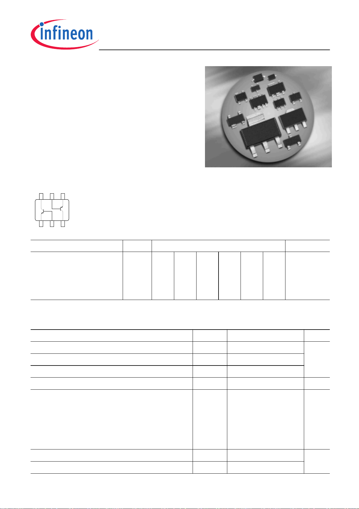
NPN Silicon Switching Transistors
g
• High DC current gain: 0.1 mA to 100 mA
• Low collector-emitter saturation voltage
• For SMBT3904S / SMBT3904U:
Two (galvanic) internal isolated transistors
with good matching in one package
• Complementary types: SMBT3906... MMBT3906
• SMBT3904S / U: For orientation in reel
see package information below
SMBT3906S/U
C1 B2 E2
6 54
SMBT3904...MMBT3904
TR1
TR2
321
C2B1E1
EHA07178
Type Marking Pin Configuration Package
SMBT3904/ MMBT3904
SMBT3904L3*
SMBT3904S
SMBT3904U
s1A
1A
s1A
s1A
1=B
1=B
1=E1
1=E1
2=E
2=E
2=B1
2=B1
3=C
3=C
3=C2
3=C2
-
-
4=E2
4=E2
-
-
5=B2
5=B2
-
-
6=C1
6=C1
SOT23
TSLP-3-4
SOT363
SC74
* Preliminary data
Maximum Ratings
Parameter
Collector-emitter voltage V
Collector-base voltage V
Emitter-base voltage V
Collector current I
Total power dissipation-
T
≤ 69°C
S
T
≤ tbd°C
S
T
≤ 115°C
S
T
≤ 105°C
S
Symbol Value Unit
40 V
60
6
200 mA
mW
C
P
CEO
CBO
EBO
tot
330
250
250
330
Junction temperature T
Storage temperature T
j
st
1
150 °C
-65 ... 150
2006-07-11
Thermal Resistance
Parameter
SMBT3904...MMBT3904
Symbol Value Unit
Junction - soldering point1)
SMBT3904/ MMBT3904
SMBT3904L3
SMBT3904S
SMBT3904U
Electrical Characteristics at T
= 25°C, unless otherwise specified
Parameter
DC Characteristics
Collector-emitter breakdown voltage
I
= 1 mA, IB = 0
C
Collector-base breakdown voltage
I
= 10 µA, IE = 0
C
Emitter-base breakdown voltage
I
= 10 µA, IC = 0
E
R
thJS
K/W
≤ 245
≤ tbd
≤ 140
≤ 135
Symbol Values Unit
min. typ. max.
V
(BR)CEO
V
(BR)CBO
V
(BR)EBO
40 - -
60 - -
6 - -
V
Collector-base cutoff current
V
= 30 V, IE = 0
CB
DC current gain2)
I
= 100 µA, VCE = 1 V
C
I
= 1 mA, VCE = 1 V
C
I
= 10 mA, VCE = 1 V
C
I
= 50 mA, VCE = 1 V
C
I
= 100 mA, VCE = 1 V
C
Collector-emitter saturation voltage2)
I
= 10 mA, IB = 1 mA
C
I
= 50 mA, IB = 5 mA
C
Base emitter saturation voltage2)
I
= 10 mA, IB = 1 mA
C
I
= 50 mA, IB = 5 mA
C
1
For calculation of R
2
Pulse test: t < 300µs; D < 2%
please refer to Application Note Thermal Resistance
thJA
I
CBO
h
FE
V
CEsat
V
BEsat
- - 50 nA
40
70
100
60
30
-
-
0.65
-
-
-
-
-
-
-
-
-
-
-
-
300
-
-
0.2
0.3
0.85
0.95
-
V
2
2006-07-11

SMBT3904...MMBT3904
Electrical Characteristics at TA = 25°C, unless otherwise specified
Parameter
AC Characteristics
Transition frequency
I
= 10 mA, VCE = 20 V, f = 100 MHz
C
Collector-base capacitance
V
= 5 V, f = 1 MHz
CB
Emitter-base capacitance
V
= 0.5 V, f = 1 MHz
EB
Delay time
V
= 3 V, IC = 10 mA, IB1 = 1 mA,
CC
V
BE(off)
= 0.5 V
Rise time
V
= 3 V, IC = 10 mA, IB1 = 1 mA,
CC
V
BE(off)
= 0.5 V
Symbol Values Unit
min. typ. max.
f
C
C
t
t
T
cb
eb
d
r
300 - - MHz
- - 3.5 pF
- - 8
- - 35 ns
- - 35
Storage time
V
= 3 V, IC = 10 mA, IB1 = I
CC
B2
Fall time
V
= 3 V, IC = 10 mA, IB1 = IB2 = 1 mA
CC
Noise figure
I
= 100 µA, VCE = 5 V, f = 1 kHz,
C
∆ f = 200 Hz, R
= 1 kΩ
S
= 1 mA
t
t
F
stg
f
- - 200
- - 50
- - 5 dB
3
2006-07-11
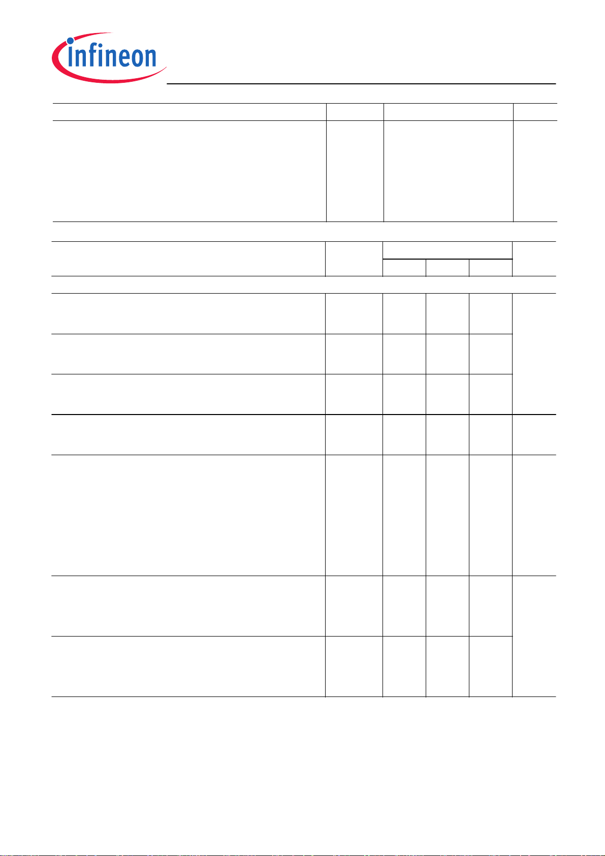
Test circuits
Delay and rise time
D = 2%300 ns
+10.9 V
0
-0.5 V
10 k
Ω
SMBT3904...MMBT3904
+3.0 V
Ω
275
C
<4.0 pF
<1.0 ns
Storage and fall time
<<
1
t
1
D = 2%
+10.9 V
0
EHN00061
+3.0 V
µs50010 t
275
Ω
10
Ω
k
C
-9.1
V
<1.0
ns
1N916
4
<4.0 pF
EHN00062
2006-07-11
SMBT3904...MMBT3904
)
DC current gain h
V
= 10 V, normalized
CE
1
10
h
FE
5
0
10
5
-1
10
-1 0 1 2
10
55
10 10 10
FE
= ƒ(I
125 C
25 C
-55 C
)
C
EHP00765
Saturation voltage I
h
= 10
FE
2
= ƒ(V
C
BEsat
; V
CEsat
EHP00756
)
mA
Ι
C
2
10
5
V
BE
10
V
CE
1
5
0
mA
10
0
2
Ι
C
0.2 0.4 0.6 0.8 1.0
V
BE sat
V,
V
1.2
CE sat
Collector-base capacitance C
Emitter-base capacitance
9
pF
)
7
EB
(C
6
CB
C
5
CEB
4
3
2
1
0
0 4 8 12 16
C
eb
= ƒ(V
cb
= ƒ(V
EB
A
VCB(V
CB
)
CCB
22
)
Total power dissipation P
SMBT3904/ MMBT3904
360
mW
300
270
240
tot
P
210
180
150
120
90
60
30
0
0 15 30 45 60 75 90 105 120
EB
= ƒ(T
tot
)
S
150
°C
T
S
5
2006-07-11

SMBT3904...MMBT3904
Total power dissipation P
SMBT3904S
300
mW
250
225
200
tot
P
175
150
125
100
75
50
25
0
0 15 30 45 60 75 90 105 120
= ƒ(T
tot
)
S
Total power dissipation P
= ƒ(T
tot
)
S
SMBT3904U
360
mW
300
270
240
tot
P
210
180
150
120
90
60
30
°C
T
150
S
0
0 15 30 45 60 75 90 105 120
°C
150
T
S
Permissible Pulse Load
P
totmax/PtotDC
= ƒ(t
)
p
SMBT3904/ MMBT3904
3
10
P
totmax
totPDC
10
10
10
2
5
1
5
0
-6
10
10-510-410-310
=
D
Permissible Puls Load R
thJS
= ƒ (t
)
p
SMBT3904S
EHP00935
t
p
t
p
T
T
D
=
0
0.005
0.01
0.02
0.05
0.1
0.2
0.5
-2
10
t
-1
100s
p
K/W
thJS
R
10
10
10
10
10
-1
3
2
1
0
10
0.5
0.2
0.1
0.05
0.02
0.01
0.005
D = 0
-6
10
-5
10
-4
10
-3
10
-2
s
t
0
10
p
6
2006-07-11

SMBT3904...MMBT3904
Permissible Pulse Load
P
totmax/PtotDC
= ƒ(t
)
p
SMBT3904S
3
10
-
totDC
/P
2
10
totmax
P
1
10
0
10
10
-6
10
-5
10
-4
10
D = 0
0.005
0.01
0.02
0.05
0.1
0.2
0.5
-3
10
Permissible Puls Load R
thJS
= ƒ (t
)
p
SMBT3904U
3
10
K/W
2
10
thJS
R
D=0.5
1
10
0
-2
s
t
0
10
p
10
10
-6
10
-5
10
0.2
0.1
0.05
0.02
0.01
0.005
0
-4
10
-3
10
-2
s
t
0
10
p
Permissible Pulse Load
P
totmax/PtotDC
= ƒ(t
)
p
SMBT3904U
2
10
totDC
/P
totmax
P
10
10
1
0
10
-6
10
D=0
0.005
0.01
0.02
0.05
0.1
0.2
0.5
-5
10
-4
10
Delay time t
Rise time
3
10
= ƒ(I
d
t
= ƒ(I
r
)
C
)
C
EHP00761
ns
t
t
,
r
d
2
10
t
r
t
d
= 10
h
FE
V
= 3 V
CC
40 V
15 V
1
10
V
= 2 V
BE
0 V
0
-3
10
-2
s
t
0
10
p
10
01 2
10
55
10 10
mA
Ι
C
10
3
7
2006-07-11

SMBT3904...MMBT3904
Storage time t
3
10
ns
t
s
2
10
1
10
0
10
01 2
10
stg
= ƒ(I
)
C
EHP00762
25 C
= 20
125 C
h
FE
10
= 20
h
FE
10
55
10 10
mA
Ι
Fall time tf = ƒ(IC)
V
h
CC
FE
EHP00763
= 40 V
= 20
mA
Ι
C
10
3
3
10
ns
t
f
25 C
125 C
2
10
= 10
h
1
10
0
3
10
C
10
01 2
10
FE
55
10 10
Rise time t
3
10
ns
t
r
125 C
2
10
1
10
0
10
01 2
10
= ƒ(I
r
)
C
25 C
55
10 10
V
h
CC
FE
EHP00764
= 40 V
= 10
mA
Ι
C
10
3
8
2006-07-11

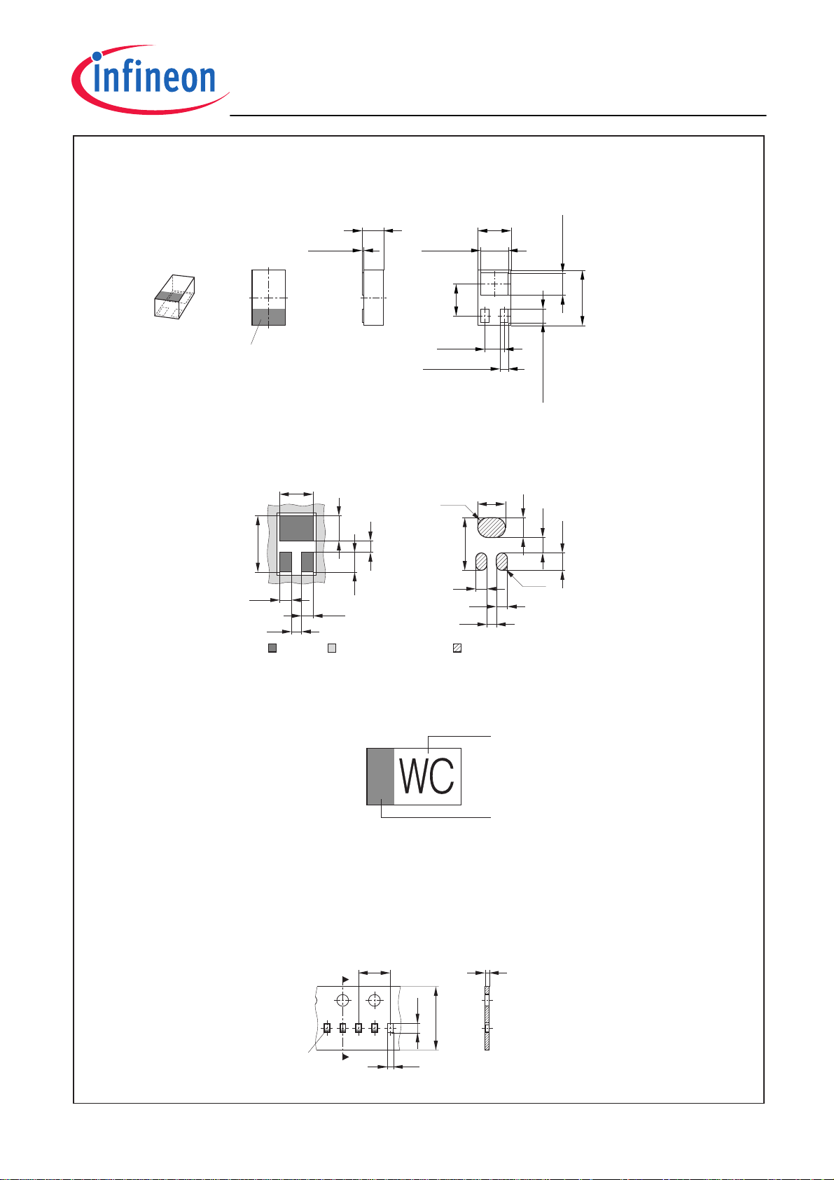
Package Outline
Foot Print
Pin 1
marking
±0.2
2.9
(2.25)
1.9
Package SC74
B
(0.35)
546
321
+0.1
0.35
-0.05
0.95
0.2
M
0.5
SMBT3904...MMBT3904
1.1 MAX.
+0.1
0.15
-0.06
±0.1
±0.1
2.5
0.25
6x
B
10˚ MAX.
0.1 MAX.
M
A0.2
±0.1
1.6
10˚ MAX.
A
0.95
Marking Layout (Example)
Small variations in positioning of
Date code, Type code and Manufacture are possible.
Pin 1 marking
Laser marking
Standard Packing
Reel ø180 mm = 3.000 Pieces/Reel
Reel ø330 mm = 10.000 Pieces/Reel
For symmetric types no defined Pin 1 orientation in reel.
4
1.9
2.9
Manufacturer
2005, June
Date code (Year/Month)
BCW66H
Type code
0.2
Pin 1
marking
3.15
9
8
2.7
1.15
2006-07-11

Package Outline
Foot Print
Package SOT23
±0.1
2.9
12
1)
+0.1
0.4
-0.05
1.9
0.25MBC
1) Lead width can be 0.6 max. in dambar area
B
3
C
0.95
0.8
0.15 MIN.
±0.15
2.4
0.2
SMBT3904...MMBT3904
±0.1
1
0.1 MAX.
±0.1
1.3
10˚ MAX.
0.08...0.15
0...8˚
M
A
10˚ MAX.
A
Marking Layout (Example)
Standard Packing
Reel ø180 mm = 3.000 Pieces/Reel
Reel ø330 mm = 10.000 Pieces/Reel
Pin 1
0.8 1.2
EH
4
0.9
s
0.9 0.91.3
Manufacturer
2005, June
Date code (YM)
BCW66
Type code
0.2
Pin 1
3.15
2.13
10
2.65
8
1.15
2006-07-11

Package Outline
Package SOT363
±0.2
2
0.2
+0.1
-0.05
5 4
6x
M
0.1
0.1 MAX.
0.1
SMBT3904...MMBT3904
±0.1
0.9
A
Pin 1
marking
1623
Foot Print
Marking Layout (Example)
+0.1
-0.05
±0.1
1.25
±0.1
2.1
0.1 MIN.
M
0.2 A
0.15
0.650.65
0.3
0.70.9
1.6
0.65
0.65
Small variations in positioning of
Date code, Type code and Manufacture are possible.
Pin 1 marking
Laser marking
Standard Packing
Reel ø180 mm = 3.000 Pieces/Reel
Reel ø330 mm = 10.000 Pieces/Reel
For symmetric types no defined Pin 1 orientation in reel.
4
Pin 1
marking
2.15
Manufacturer
2005, June
Date code (Year/Month)
BCR108S
Type code
0.2
8
2.3
1.1
11
2006-07-11
Package Outline
Package TSLP-3-4
SMBT3904...MMBT3904
Top view
+0.1
0.4
0.05 MAX.
1
3
2
Pin 1
marking
±0.035
0.5
0.35
2x0.15
Bottom view
0.6
1)
3
±0.05
2
0.575
±0.05
±0.035
±0.05
1)
1
1)
±0.035
0.25
1) Dimension applies to plated terminal
2x
Foot Print
For board assembly information please refer to Infineon website "Packages"
1
0.225
0.15
0.6
0.45
0.225
R0.19
0.2
0.35
0.2
0.17
0.5
0.38
0.255
0.95
R0.1
0.2
1)
±0.035
0.4
0.315
±0.05
1
Marking Layout (Example)
Standard Packing
Reel ø180 mm = 15.000 Pieces/Reel
Stencil aperturesCopper Solder mask
BCR133L3
Type code
Pin 1 marking
Laser marking
4
1.16
8
0.5
Pin 1
marking
0.76
12
2006-07-11

SMBT3904...MMBT3904
Edition 2006-02-01
Published by
Infineon Technologies AG
81726 München, Germany
© Infineon Technologies AG 2006.
All Rights Reserved.
Attention please!
The information given in this dokument shall in no event be regarded as a guarantee
of conditions or characteristics (“Beschaffenheitsgarantie”). With respect to any
examples or hints given herein, any typical values stated herein and/or any information
regarding the application of the device, Infineon Technologies hereby disclaims any
and all warranties and liabilities of any kind, including without limitation warranties of
non-infringement of intellectual property rights of any third party.
Information
For further information on technology, delivery terms and conditions and prices
please contact your nearest Infineon Technologies Office (www.infineon.com).
Warnings
Due to technical requirements components may contain dangerous substances.
For information on the types in question please contact your nearest
Infineon Technologies Office.
Infineon Technologies Components may only be used in life-support devices or
systems with the express written approval of Infineon Technologies, if a failure of
such components can reasonably be expected to cause the failure of that
life-support device or system, or to affect the safety or effectiveness of that
device or system.
Life support devices or systems are intended to be implanted in the human body,
or to support and/or maintain and sustain and/or protect human life. If they fail,
it is reasonable to assume that the health of the user or other persons
may be endangered.
13
2006-07-11
 Loading...