

PNP Silicon Switching Transistor
• High DC current gain: 0.1 mA to 500 mA
SMBT2907A/MMBT2907A
• Low collector-emitter saturation voltage
3
• Complementary type:
SMBT2222A / MMBT2222A (NPN)
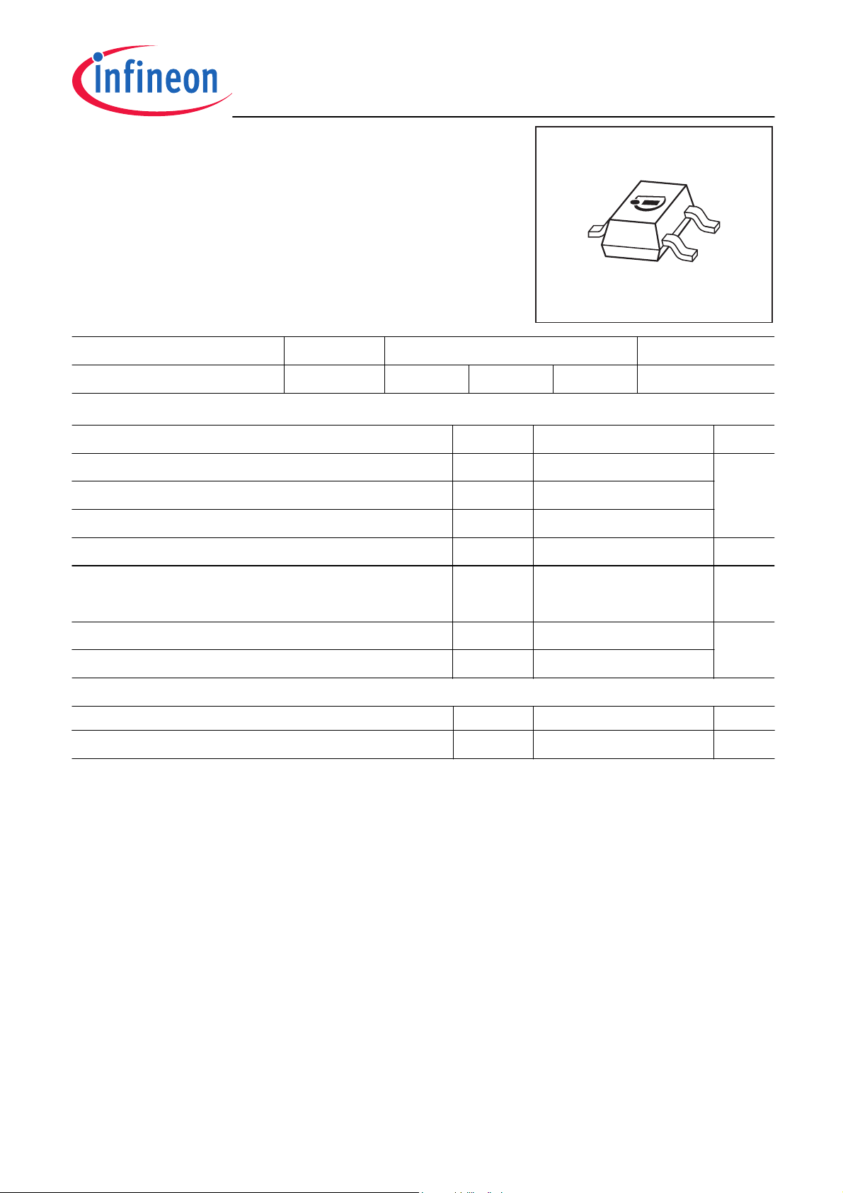
Type Marking Pin Configuration Package
SMBT2907A/MMBT2907A s2F
1 = B 2 = E 3 = C
SOT23
Maximum Ratings
Parameter
Collector-emitter voltage V
Collector-base voltage V
Emitter-base voltage V
Collector current I
Total power dissipation-
≤ 77 °C
T
S
Junction temperature T
Symbol Value Unit
60 V
60
5
600 mA
330 mW
150 °C
C
P
CEO
CBO
EBO
tot
j
2
1
Storage temperature T
stg
-65 ... 150
Thermal Resistance
Parameter Symbol Value Unit
Junction - soldering point
1
For calculation of R
please refer to Application Note Thermal Resistance
thJA
1)
R
thJS
≤ 220
K/W
1
2006-03-20

SMBT2907A/MMBT2907A
Electrical Characteristics at T
= 25°C, unless otherwise specified
Parameter Symbol Values Unit
min. typ. max.
DC Characteristics
Collector-emitter breakdown voltage
I
= 10 mA, IB = 0
C
Collector-base breakdown voltage
I
= 10 µA, IE = 0
C
Emitter-base breakdown voltage
I
= 10 µA, IC = 0
E
Collector-base cutoff current
V
= 50 V, IE = 0
CB
V
= 50 V, IE = 0 , TA = 150 °C
CB
Emitter-base cutoff current
V
= 5 V, IC = 0
EB
DC current gain1)
I
= 100 µA, VCE = 10 V
C
I
= 1 mA, VCE = 10 V
C
V
(BR)CEO
V
(BR)CBO
V
(BR)EBO
I
CBO
I
EBO
h
FE
60 - -
60 - -
5 - -
-
-
-
-
0.01
10
- - 10 nA
75
100
-
-
-
-
V
µA
-
I
= 10 mA, VCE = 10 V
C
I
= 150 mA, VCE = 10 V
C
I
= 500 mA, VCE = 10 V
C
Collector-emitter saturation voltage1)
I
= 150 mA, IB = 15 mA
C
I
= 500 mA, IB = 50 mA
C
Base emitter saturation voltage-1)
I
= 150 mA, IB = 15 mA
C
I
= 500 mA, IB = 50 mA
C
1
Puls test: t ≤ 300µs, D = 2%
V
CEsat
V
BEsat
100
100
50
-
-
-
-
-
-
-
-
-
-
-
-
300
-
0.4
1.6
1.3
2.6
V
2
2006-03-20

SMBT2907A/MMBT2907A
Electrical Characteristics at TA = 25°C, unless otherwise specified
Parameter
AC Characteristics
Transition frequency
= 20 mA, VCE = 20 V, f = 100 MHz
I
C
Collector-base capacitance
= 10 V, f = 1 MHz
V
CB
Emitter-base capacitance
V
= 0.5 V, f = 1 MHz
EB
Delay time
V
= 30 V, IC = 150 mA, IB1 = 15 mA,
CC
V
BE(off)
= 0.5 V
Rise time
= 30 V, IC = 150 mA, IB1 = 15 mA,
V
CC
V
BE(off)
= 0.5 V
Symbol Values Unit
min. typ. max.
f
C
C
t
t
T
cb
eb
d
r
200 - - MHz
- - 8 pF
- - 30
- - 10 ns
- - 40
Storage time
= 30 V, IC = 150 mA, IB1 = IB2 = 15mA
V
CC
Fall time
= 30 V, IC = 150 mA, IB1 = IB2 = 15mA
V
CC
t
t
stg
f
- - 80
- - 30
3
2006-03-20

Test circuit
Delay and rise time
SMBT2907A/MMBT2907A
-30ΩV
200
Input
Z
0
t
< 2ns
r
= 50
Ω
0
-16 V
ns200
Storage and fall time
50
1
k
Ω
Ω
+15 V
Osc.
t
r
EHN00053
V
-30
200
< 5 ns
Ω
Input
Z
= 50
0
t
< 2 ns
r
Ω
1
Ωk
0
V
-30
50
Ω
200 ns
Oscillograph: R > 100, C < 12pF, tr < 5ns
Osc.
1 Ω
k
t
< 5 ns
r
EHN00069
4
2006-03-20

SMBT2907A/MMBT2907A
0
DC current gain hFE = ƒ(IC)
= 5 V
V
CE
3
10
5
h
FE
150 ˚C
25 ˚C
2
10
5
1
10
-1 0 1 2 3
10
10 10 10
-50 ˚C
Saturation voltage IC = ƒ(V
= 10
h
FE
EHP00754SMBT 2907/A
10
3
BEsat
; V
CEsat
EHP00750SMBT 2907/A
)
mA
Ι
C
10
V
2
CE
V
BE
5
1
10
5
0
10
5
-2
10
-1
mA
10
10
Ι
C
0.2 0.4 0.6 0.8 1.0
0
V
BE sat
1.2
V
V,
CE sat
1.6
Transition frequency fT = ƒ(IC)
= 5 V
V
CE
3
10
MHz
5
f
T
2
10
5
1
10
0123
10 10
555
10
Ι
mA
C
Collector-base capacitance C
Emitter-base capacitance C
EHP00749SMBT 2907/A
10
30
pF
26
24
22
20
CCB0(CEB0)
18
16
14
12
10
8
6
4
2
0 4 8 12 16
CEB
cb
= ƒ(V
eb
= ƒ(V
EB
V
VCB0(VEB
CB
)
CCB
)
22
5
2006-03-20

SMBT2907A/MMBT2907A
Collector-base capacitance CCB= ƒ (VCB)
f = 1MHz
2
10
pF
5
C
cb
1
10
5
0
10
-1 0 1 2
10 10
555
10
EHP00747SMBT 2907/A
V
V
CB
10
Total power dissipation P
360
mW
300
270
240
tot
P
210
180
150
120
90
60
30
0
0 15 30 45 60 75 90 105 120
= ƒ(TS)
tot
°C
T
150
S
Permissible Pulse Load
P
totmax/PtotDC
3
10
P
tot max
5
totPDC
2
10
5
1
10
5
0
10
10
= ƒ(tp)
=
D
-6
10-510-410-310
Delay time td = ƒ(IC)
Rise time t
EHP00748SMBT 2907/A
t
p
t
p
T
T
D
=
0
0.005
0.01
0.02
0.05
0.1
0.2
0.5
-2
s
t
p
10
0
10
ns
5
,
t
t
r
d
10
5
10
= ƒ(IC)
r
3
= 0 V
V
BE
VV, = 30 V
BE
t
r
2
1
10
t
d
01 2
5 5
10 10
, = 10 V
= 20 V
V ,
CC
CC
mA
Ι
C
EHP00751SMBT 2907/A
3
5
10
6
2006-03-20

SMBT2907A/MMBT2907A
Storage time t
3
10
ns
t
stg
5
2
10
5
10
h = 10
FE
1
01 2
10
= ƒ(IC)
stg
= 20
h
FE
5 5
10 10
mA
Ι
Fall time tf = ƒ(IC)
EHP00752SMBT 2907/A
3
10
ns
t
f
5
= 20h
FE
h = 10
FE
2
10
5
1
3
5
10
C
10
01 2
10
5 5
10 10
EHP00753SMBT 2907/A
VCC= 30 V
5
mA
Ι
C
10
3
7
2006-03-20

Package Outline
Foot Print
Package SOT23
±0.1
2.9
12
1)
+0.1
0.4
-0.05
1.9
0.25MBC
1) Lead width can be 0.6 max. in dambar area
B
3
C
0.95
0.8
0.15 MIN.
±0.15
2.4
0.2
SMBT2907A/MMBT2907A
±0.1
1
0.1 MAX.
±0.1
1.3
10˚ MAX.
0.08...0.15
0...8˚
M
A
10˚ MAX.
A
Marking Layout
12
Pin 1
s
Standard Packing
Reel ø180 mm = 3.000 Pieces/Reel
Reel ø330 mm = 10.000 Pieces/Reel
0.8 1.2
Manufacturer
Date code (Year/Month)
Type code
4
0.9
0.9 0.91.3
EH
Example
0.2
s
2003, July
37
BCW66
Pin 1
3.15
2.13
8
2.65
8
1.15
2006-03-20

SMBT2907A/MMBT2907A
Published by
Infineon Technologies AG
81726 München, Germany
© Infineon Technologies AG 2006.
All Rights Reserved.
Attention please!
The information given in this data sheet shall in no event be regarded as a guarantee
of conditions or characteristics (“Beschaffenheitsgarantie”). With respect to any
examples or hints given herein, any typical values stated herein and/or any information
regarding the application of the device, Infineon Technologies hereby disclaims any
and all warranties and liabilities of any kind, including without limitation warranties of
non-infringement of intellectual property rights of any third party.
Information
For further information on technology, delivery terms and conditions and prices
please contact your nearest Infineon Technologies Office (www.infineon.com).
Warnings
Due to technical requirements components may contain dangerous substances.
For information on the types in question please contact your nearest
Infineon Technologies Office.
Infineon Technologies Components may only be used in life-support devices or
systems with the express written approval of Infineon Technologies, if a failure of
such components can reasonably be expected to cause the failure of that
life-support device or system, or to affect the safety or effectiveness of that
device or system.
Life support devices or systems are intended to be implanted in the human body,
or to support and/or maintain and sustain and/or protect human life. If they fail,
it is reasonable to assume that the health of the user or other persons
may be endangered.
9
2006-03-20
 Loading...