

SKP10N60A, SKB10N60A
SKW10N60A
Fast IGBT in NPT-technology with soft, fast recovery anti-parallel EmCon diode
• 75% lower E
combined with low conduction losses
compared to previous generation
off
C
• Short circuit withstand time – 10 µs
• Designed for:
- Motor controls
- Inverter
G
E
• NPT-Technology for 600V applications offers:
- very tight parameter distribution
- high ruggedness, temperature stable behaviour
- parallel switching capability
P-TO-220-3-1
(TO-220AB)
P-TO-263-3-2 (D²-PAK)
(TO-263AB)
P-TO-247-3-1
(TO-247AC)
• Very soft, fast recovery anti-parallel EmCon diode
• Complete product spectrum and PSpice Models : http://www.infineon.com/igbt/
Type
V
CE
SKP10N60A 600V 10A 2.3V
I
C
V
CE(sat)
T
j
150°C
Package Ordering Code
TO-220AB Q67040-S4458
SKB10N60A TO-263AB Q67040-S4459
SKW10N60A TO-247AC Q67040-S4506
Maximum Ratings
Parameter Symbol
Collector-emitter voltage
DC collector current
= 25°C
T
C
T
= 100°C
C
Pulsed collector current, tp limited by T
jmax
Turn off safe operating area
≤ 600V, Tj ≤ 150°C
V
CE
Diode forward current
= 25°C
T
C
= 100°C
T
C
Diode pulsed current, tp limited by T
jmax
Gate-emitter voltage
Short circuit withstand tim e
VGE = 15V, V
≤ 600V, Tj ≤ 150°C
CC
1)
Power dissipation
= 25°C
T
C
Operating junction and storage temperature
V
CE
I
C
I
Cpuls
-
I
F
I
Fpuls
V
GE
t
SC
P
tot
T
j
, T
stg
Value
SKP10N60A
SKB10N60A
SKW10N60A
600 V
20
10.6
40
40
21
10
42
±20
10
92
-55...+150
Unit
A
V
µs
W
°C
1)
Allowed number of short circuits: <1000; time between short circuits: >1s.
1Jul-02

SKP10N60A, SKB10N60A
Thermal Resistance
Parameter Symbol Conditions
Characteristic
IGBT thermal resistance,
junction – case
Diode thermal resistance,
junction – case
Thermal resistance,
junction – ambient
SMD version, device on PCB
1)
Electrical Characteristic, at Tj = 25 °C, unless otherwise specified
Parameter Symbol Conditions
Static Characteristic
Collector-emitter breakdown voltage
Collector-emitter saturation voltage
Diode forward voltage
Zero gate voltage collector current
Gate-emitter leakage current
Transconductance
Dynamic Characteristic
Input capacitance
Output capacitance
Reverse transfer capacitance
Gate charge
Internal emitter inductance
measured 5mm (0.197 in.) from case
Short circuit collector current
2)
R
thJC
R
thJCD
R
thJA
R
thJA
V
(BR)CES
V
CE(sat)VGE
V
F
I
CES
I
GES
g
fs
C
iss
C
oss
C
rss
Q
Gate
L
E
I
C(SC)
TO-220AB
TO-247AC
TO-263AB 40
VGE=0V, IC=500µA
= 15V, IC=10A
T
=25°C
j
=150°C
T
j
VGE=0V, IF=10A
T
=25°C
j
=150°C
T
j
VCE=600V,VGE=0V
=25°C
T
j
T
=150°C
j
VCE=0V,VGE=20V
VCE=20V, IC=10A
VCE=25V,
=0V,
V
GE
f=1MHz
VCC=480V, IC=10A
V
=15V
GE
TO-220AB
TO-247AC
VGE=15V,tSC≤10µs
V
≤ 600V,
CC
T
≤ 150°C
j
SKW10N60A
Max. Value
SKP10N60A
SKB10N60A
SKW10n60A
1.35
2.4
62
40
Value
min. Typ. max.
600 - -
1.7
-
1.2
-
-
-
2
2.3
1.4
1.25
-
-
2.4
2.8
1.8
1.65
40
1500
- - 100 nA
-6.7-S
- 550 660
-6275
-4251
-5268nC
-
-
7
13
- 100 - A
Unit
K/W
Unit
V
µA
pF
-
nH
-
1)
Device on 50mm*50mm*1.5mm epoxy PCB FR4 with 6cm2 (one layer, 70µm thick) copper area for
collector connection. PCB is vertical without blown air.
2)
Allowed number of short circuits: <1000; time between short circuits: >1s.
2Jul-02

SKP10N60A, SKB10N60A
Switching Characteristic, Inductive Load, at Tj=25 °C
Parameter Symbol Conditions
IGBT Characteristic
Turn-on delay time
Rise time
Turn-off delay time
Fall time
Turn-on energy
Turn-off energy
Total switching energy
Anti-Parallel Diode Characteri sti c
Diode reverse recovery time
Diode reverse recovery charge
Diode peak reverse recovery current
Diode peak rate of fall of reverse
recovery current during t
b
t
d(on)
t
r
t
d(off)
t
f
E
on
E
off
E
ts
t
rr
t
S
t
F
Q
rr
I
rrm
dirr/dt
Tj=25°C,
V
=400V,IC=10A,
CC
V
=0/15V,
GE
R
=25Ω,
G
1)
L
=180nH,
σ
1)
C
=55pF
σ
Energy losses include
“tail” and diode
reverse recovery.
=25°C,
T
j
V
=200V, IF=10A,
R
di
/dt=200A/µs
F
SKW10N60A
Value
min. typ. max.
-2834
-1215
- 178 214
-2429
- 0.15 0.173
- 0.17 0.221
- 0.320 0.394
-
-
-
220
20
200
- 310 - nC
-4.5-A
- 180 -
Unit
ns
mJ
-
ns
-
-
A/µs
Switching Characteristic, Inductive Load, at Tj=150 °C
Parameter Symbol Conditions
IGBT Characteristic
Turn-on delay time
Rise time
Turn-off delay time
Fall time
Turn-on energy
Turn-off energy
Total switching energy
t
d(on)
t
r
t
d(off)
t
f
E
on
E
off
E
ts
Tj=150°C
V
=400V,IC=10A,
CC
V
=0/15V,
GE
R
=25Ω
G
1)
L
=180nH,
σ
1)
C
=55pF
σ
Energy losses include
“tail” and diode
reverse recovery.
Anti-Parallel Diode Characteri sti c
Diode reverse recovery time
Diode reverse recovery charge
Diode peak reverse recovery current
Diode peak rate of fall of reverse
recovery current during t
b
t
rr
t
S
t
F
Q
rr
I
rrm
dirr/dt
=150°C
T
j
V
=200V, IF=10A,
R
di
/dt=200A/µs
F
Value
min. typ. max.
-2834
Unit
ns
-1215
- 198 238
-2632
- 0.260 0.299
mJ
- 0.280 0.364
- 0.540 0.663
-
-
-
350
36
314
-
ns
-
-
- 690 - nC
-6.3-A
- 200 -
A/µs
1)
Leakage inductance L
a n d Stray capacity Cσ due to dynamic test circuit in Figure E.
σ
3Jul-02
SKP10N60A, SKB10N60A
z
SKW10N60A
50A
I
c
TC=80°c
40A
30A
20A
, COLLECTOR CURRENT
I
C
10A
TC=110°c
I
c
0A
10Hz 100Hz 1kHz 10kHz 100kH
f, SWITCHING FREQUENCY VCE, COLLECTOR-EMITTER VOLTAGE
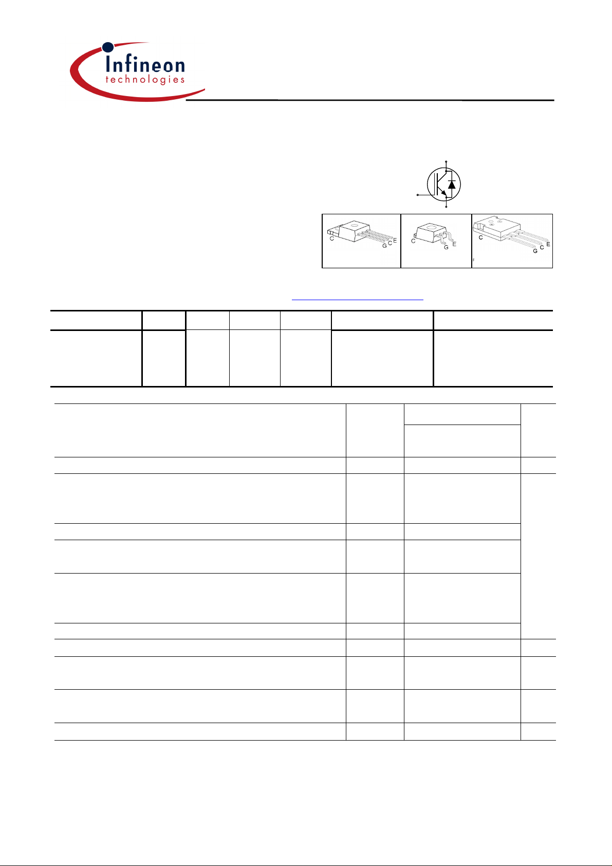
Figure 1. Collector current as a function of
switching frequency
(T
≤ 150°C, D = 0.5, VCE = 400V,
j
V
= 0/+15V, RG = 25Ω)
GE
, COLLECTOR CURRENT
I
C
10A
1A
0,1A
1V 10V 100V 1000V
Figure 2. Safe operating area
(D = 0, T
= 25°C, Tj ≤ 150°C)
C
tp=5µs
15µs
50µs
200µs
1ms
DC
120W
100W
80W
60W
40W
, POWER DISSIPATION
tot
P
20W
0W
25°C 50°C 75°C 100°C 125°C
TC, CASE TEMPERATURE TC, CASE TEMPERATURE
Figure 3. Power dissipation as a function
of case temperature
(T
≤ 150°C)
j
25A
20A
15A
10A
, COLLECTOR CURRENT
C
I
5A
0A
25°C 50°C 75°C 100°C 125°C
Figure 4. Collector current as a function of
case temperature
(VGE ≤ 15V, Tj ≤ 150°C)
4Jul-02
SKP10N60A, SKB10N60A
SKW10N60A
35A
30A
25A
VGE=20V
20A
15A
10A
, COLLECTOR CURRENT
C
I
5A
0A
0V 1V 2V 3V 4V 5V
15V
13V
11V
9V
7V
5V
VCE, COLLECTOR-EMITTER VOLTAGE VCE, COLLECTOR-EMITTER VOLTAGE
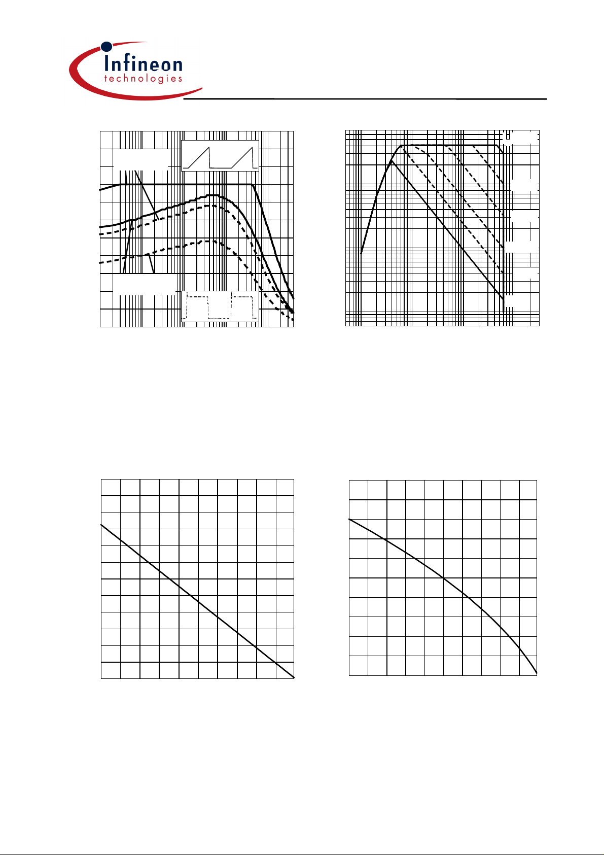
Figure 5. Typical output characteristics
(T
= 25°C)
j
35A
30A
25A
VGE=20V
20A
15A
10A
, COLLECTOR CURRENT
C
I
5A
0A
0V 1V 2V 3V 4V 5V
15V
13V
11V
9V
7V
5V
Figure 6. Typical output characteristics
(Tj = 150°C)
35A
30A
25A
20A
15A
10A
, COLLECTOR CURRENT
C
I
5A
0A
0V 2V 4V 6V 8V 10V
Tj=+25°C
+150°C
VGE, GATE-EMITTER VOLTAGE Tj, JUNCTION TEMPERATURE
Figure 7. Typical transfer characteristics
(V
= 10V)
CE
3,5V
IC=20A
3,0V
2,5V
IC=10A
2,0V
IC=5A
, COLLECTOR-EMITTER SATURATION VOLT AGE
1,5V
CE(sat)
V
0°C 50°C 100°C 150°C
Figure 8. Typical collector-emitter
saturation voltage as a function of junction
temperature
(V
= 15V)
GE
5Jul-02

SKP10N60A, SKB10N60A
A
SKW10N60A
t
d(off)
100ns
t, SWITCHING TIMES
10ns
0A 5A 10A 15A 20A 25
IC, COLLECTOR CURRENT RG, GATE RESIST OR
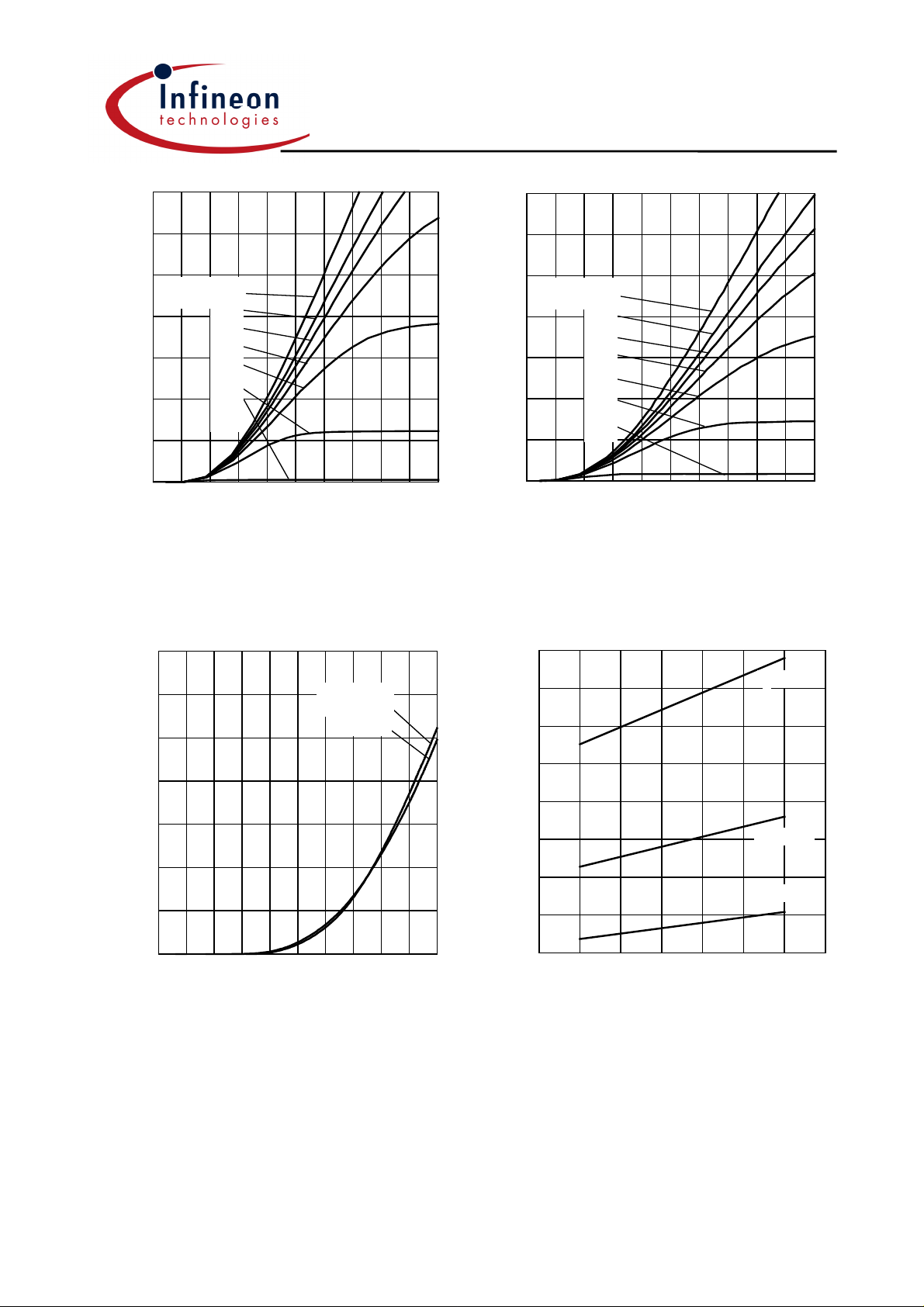
Figure 9. Typical switching times as a
function of collector current
(inductive load, T
V
= 0/+15V, RG = 25Ω,
GE
= 150°C, VCE = 400V,
j
Dynamic test circuit in Figure E)
t
f
t
d(on)
t
r
t
100ns
t, SWITCHING TIMES
10ns
d(off)
t
f
t
d(on)
t
r
0Ω 20Ω 40 Ω 60Ω 80Ω
Figure 10. Typical switching times as a
function of gate resistor
(inductive load, T
V
= 0/+15V, IC = 10A,
GE
= 150°C, VCE = 400V,
j
Dynamic test circuit in Figure E)
5,5V
t
d(off)
100ns
t
d(on)
t, SWITCHING TIMES
t
f
t
10ns
r
0°C 50°C 100°C 150°C
Tj, JUNCTION TEMPERATURE Tj, JUNCTION TEMPERATURE
Figure 11. Typical switching times as a
function of junction temperature
(inductive load, V
I
= 10A, RG = 25Ω,
C
= 400V, VGE = 0/+15V,
CE
Dynamic test circuit in Figure E)
5,0V
4,5V
4,0V
3,5V
3,0V
2,5V
2,0V
, GATE-EMITTER THRESHOLD VOLTAGE
1,5V
GE(th)
V
1,0V
-50°C 0 °C 50°C 100°C 150°C
Figure 12. Gate-emitter threshold voltage
as a function of junction temperature
= 0.3mA)
(I
C
max.
typ.
min.
6Jul-02

SKP10N60A, SKB10N60A
E
E
E
E
τ
τ
SKW10N60A
E, SWITCHING ENERGY LOSSES
1,6mJ
1,4mJ
1,2mJ
1,0mJ
0,8mJ
0,6mJ
0,4mJ
0,2mJ
0,0mJ
*)
and
on
due to diode recovery.
0A 5A 10A 15A 20A 25A
include losses
ts
IC, COLLECTOR CURRENT RG, GATE RESISTOR
Figure 13. Typical switching energy losses
as a function of collector current
(inductive load, T
V
= 0/+15V, RG = 25Ω,
GE
= 150°C, VCE = 400V,
j
Dynamic test circuit in Figure E)
Ets*
Eon*
E
off
1,0mJ
0,8mJ
0,6mJ
0,4mJ
*)
and
on
due to diode recovery.
include losses
ts
E, SWITCHING ENERGY LOSSES
0,2mJ
0Ω 20Ω 40Ω 60Ω 80Ω
Figure 14. Typical switching energy losses
as a function of gate resistor
(inductive load, T
V
= 0/+15V, IC = 10A,
GE
= 150°C, VCE = 400V,
j
Dynamic test circuit in Figure E)
Ets*
E
off
Eon*
0,8mJ
*) Eon and Ets include losses
due to diode recovery.
0,6mJ
0,4mJ
Ets*
0,2mJ
E, SWITCHING ENERGY LOSSES
0,0mJ
Figure 15. Typical switching energy losses
as a function of junction temperature
(inductive load, V
I
= 10A, RG = 25Ω,
C
Dynamic test circuit in Figure E)
E
off
Eon*
0°C 50°C 100°C 150°C
Tj, JUNCTION TEMPERATURE
= 400V, VGE = 0/+15V,
CE
0
K/W
10
D=0.5
0.2
, TRANSIENT THERMAL IMPEDANCE
thJC
Z
10
10
10
-1
-2
-3
0.1
K/W
0.05
0.02
0.01
K/W
single pulse
K/W
1µs 10µs 100µs 1ms 10ms 100ms 1s
R,(K/W)
0.4287 0.0358
0.4830 4.3*10
0.4383 3.46*10
R
1
C1=
1/R1
C2=
tp, PULSE WIDTH
Figure 16. IGBT transient thermal
impedance as a function of pulse width
/ T)
(D = t
p
τ
, (s)
2/R2
-3
-4
R
2
7Jul-02

SKP10N60A, SKB10N60A
V
µ
SKW10N60A
25V
20V
15V
10V
120V
, GATE-EMITTER VOLTAG E
GE
5V
V
0V
0nC 25nC 50nC 75nC
QGE, GATE CHARGE VCE, COLLECTOR-EMITTER VOLTAGE
Figure 17. Typical gate charge
(I
= 10A)
C
480V
1nF
100pF
C, CAPACITANCE
10pF
0V 10V 20V 30V
Figure 18. Typical capacitance as a
function of collector-emitter voltage
(V
= 0V, f = 1MHz)
GE
C
iss
C
oss
C
rss
25
s
20
µs
µs
15
µs
10
5µ s
, SHORT CIRCUIT WITHSTAND TIME
sc
t
0µ s
10V 11V 12V 13V 14V 15
VGE, GATE-EMITTER VOLTAGE VGE, GATE-EMITTER VOLTAGE
Figure 19. Short circuit withstand time as a
function of gate-emitter voltage
(V
= 600V, start at Tj = 25°C)
CE
200A
150A
100A
50A
, SHORT CIRCUIT COLLECTOR CURRENT
C(sc)
I
0A
10V 12V 14V 16V 18V 20V
Figure 20. Typical short circuit collector
current as a function of gate-emitter voltage
(VCE ≤ 600V, Tj = 150°C)
8Jul-02

SKP10N60A, SKB10N60A
SKW10N60A
500ns
400ns
300ns
200ns
IF = 20A
IF = 10A
IF = 5A
100ns
, REVERSE RECOVERY TIME
rr
t
0ns
100A/µs 300A/µs 500A/µs 700A/µs 900A/µs
diF/dt, DIODE CURRENT SLOPE diF/dt, DIODE CURRENT SLOPE
Figure 21. Typical reverse recovery time as
a function of diode current slope
= 200V, Tj = 125°C,
(V
R
Dynamic test circuit in Figure E)
1400nC
1200nC
IF = 20A
1000nC
IF = 10A
IF = 5A
, REVERSE RECOVERY CHARGE
rr
Q
800nC
600nC
400nC
200nC
0nC
100A/µs 300A/µs 500A/µs 700A/µs 900A/µs
Figure 22. Typical reverse recovery charge
as a function of diode current slope
(VR = 200V, Tj = 125°C,
Dynamic test circuit in Figure E)
20A
16A
12A
IF = 10A
8A
4A
, REVERSE RECOVERY CURRENT
rr
I
0A
100A/µs 300A/µs 500A/µs 700A/µs900A/µs
IF = 20A
IF = 5A
diF/dt, DIODE CURRENT SLOPE diF/dt, DIODE CURRENT SLOPE
Figure 23. Typical reverse recovery current
as a function of diode current slope
(V
= 200V, Tj = 125°C,
R
Dynamic test circuit in Figure E)
000A/µs
µs
800A/
µs
600A/
µs
400A/
µs
200A/
/dt, DIODE PEAK RATE OF FALL
rr
OF REVERSE RECOVERY CURRENT
di
0A/µs
100A/µs 300A/µs 500A/µs700A/µs 900A/µs
Figure 24. Typical diode peak rate of fall of
reverse recovery current as a function of
diode current slope
(V
= 200V, Tj = 125°C,
R
Dynamic test circuit in Figure E)
9Jul-02

SKP10N60A, SKB10N60A
A
τ
τ
SKW10N60A
20A
15A
150°C
10A
100°C
, FORWARD CURRENT
F
5A
I
25°C
-55°C
0A
0.0V 0.5V 1.0V 1.5V 2.0V
VF, FORWARD VOLTAGE Tj, JUNCTION TEMPERATURE
Figure 25. Typical diode forward current as
a function of forward voltage
2.0V
IF = 20
1.5V
IF =
, FORWARD VOLTAGE
F
V
1.0V
-40°C 0°C 40°C 80°C 120°C
Figure 26. Typical diode forward voltage as
a function of junction temperature
D=0.5
0
K/W
10
0.2
0.1
R,(K/W)
0.759 5.53*10
0.481 4.28*10
0.609 4.83*10
0.551 5.77*10
R
1
C1=
1/R1
C2=
, TRANSIENT THERMAL IMPEDANCE
thJCD
Z
0.05
-1
0.02
K/W
10
0.01
single pulse
K/W
1µs 10µs 100µs 1ms 10ms 100ms 1s
10
-2
tp, PULSE WIDTH
Figure 27. Diode transient thermal
impedance as a function of pulse width
(D = t
/ T)
p
τ
, (s)
2/R2
-2
-3
-4
-5
R
2
10 Jul-02

SKP10N60A, SKB10N60A
SKW10N60A
TO-220AB
TO-263AB (D2Pak)
dimensions
symbol
A 9.70 10.30 0.3819 0.4055
B 14.88 15.95 0.5858 0.6280
C 0.65 0.86 0.0256 0.0339
D 3.55 3.89 0.1398 0.1531
E 2.60 3.00 0.1024 0.1181
F 6.00 6.80 0.2362 0.2677
G 13.00 14.00 0.5118 0.5512
H 4.35 4.75 0.1713 0.1870
K 0.38 0.65 0.0150 0.0256
L 0.95 1.32 0.0374 0.0520
M 2.54 typ. 0.1 typ.
N 4.30 4.50 0.1693 0.1772
P 1.17 1.40 0.0461 0.0551
T 2.30 2.72 0.0906 0.1071
symbol
A 9.80 10.20 0.3858 0.4016
B 0.70 1.30 0.0276 0.0512
C 1.00 1.60 0.0394 0.0630
D 1.03 1.07 0.0406 0.0421
E 2.54 typ. 0.1 typ.
F 0.65 0.85 0.0256 0.0335
G 5.08 typ. 0.2 typ.
H 4.30 4.50 0.1693 0.1772
K 1.17 1.37 0.0461 0.0539
L 9.05 9.45 0.3563 0.3720
M 2.30 2.50 0.0906 0.0984
N 15 typ. 0.5906 typ.
P 0.00 0.20 0.0000 0.0079
Q 4.20 5.20 0.1654 0.2047
R 8° max 8° max
S 2.40 3.00 0.0945 0.1181
T 0.40 0.60 0.0157 0.0236
U 10.80 0.4252
V 1.15 0.0453
W 6.23 0.2453
X 4.60 0.1811
Y 9.40 0.3701
Z 16.15 0.6358
[mm] [inch]
min max min max
dimensions
[mm] [inch]
min max min max
11 Jul-02

SKP10N60A, SKB10N60A
SKW10N60A
TO-247AC
dimensions
symbol
A 4.78 5.28 0.1882 0.2079
B 2.29 2.51 0.0902 0.0988
C 1.78 2.29 0.0701 0.0902
D 1.09 1.32 0.0429 0.0520
E 1.73 2.06 0.0681 0.0811
F 2.67 3.18 0.1051 0.1252
G 0.76 max 0.0299 max
H 20.80 21.16 0.8189 0.8331
K 15.65 16.15 0.6161 0.6358
L 5.21 5.72 0.2051 0.2252
M 19.81 20.68 0.7799 0.8142
N 3.560 4.930 0.1402 0.1941
∅P
Q 6.12 6.22 0.2409 0.2449
[mm] [inch]
min max min max
3.61 0.1421
12 Jul-02

SKP10N60A, SKB10N60A
τ
τ
τ
SKW10N60A
i,v
+
di /dt
F
I
F
t=t t
rr S F
Q=Q Q
rr S F
t
rr
t
S
+
t
F
Figure A. Definition of switching times
Q
Q
S
I
rrm
F
90% I
Figure C. Definition of diodes
switching characteristics
2
2
p(t)
1
rrrr
1
T(t)
j
12 n
Figure D. Thermal equivalent
circuit
10% I
di /dt
rr
rrm
n
n
t
rrm
V
R
rr
T
C
Figure B. Definition of switching losses
Figure E. Dynamic test circuit
Leakage inductance L
and Stray capacity C
=180nH
σ
=55pF.
σ
Published by
Infineon Technologies AG,
13 Jul-02

SKP10N60A, SKB10N60A
SKW10N60A
Bereich Kommunikation
St.-Martin-Strasse 53,
D-81541 München
© Infineon Technologies AG 2001
All Rights Reserved.
Attention please!
The information herein is given to describe certain components and shall not be considered as warranted characteristics.
Terms of delivery and rights to technical change reserved.
We hereby disclaim any and all warranties, including but not limited to warranties of non-infringement, regarding circuits,
descriptions and charts stated herein.
Infineon Technologies is an approved CECC manufacturer.
Information
For further information on technology, delivery terms and conditions and prices please contact your nearest Infineon
Technologies Office in Germany or our Infineon Technologies Representatives worldwide (see address list).
Warnings
Due to technical requirements components may contain dangerous substances. For information on the types in question
please contact your nearest Infineon Technologies Office.
Infineon Technologies Components may only be used in life-support devices or systems with the express written
approval of Infineon Technologies, if a failure of such components can reasonably be expected to cause the failure of
that life-support device or system, or to affect the safety or effectiveness of that device or system. Life support devices or
systems are intended to be implanted in the human body, or to support and/or maintain and sustain and/or protect
human life. If they fail, it is reasonable to assume that the health of the user or other persons may be endangered.
14 Jul-02
 Loading...