SGP30N60
SGW30N60
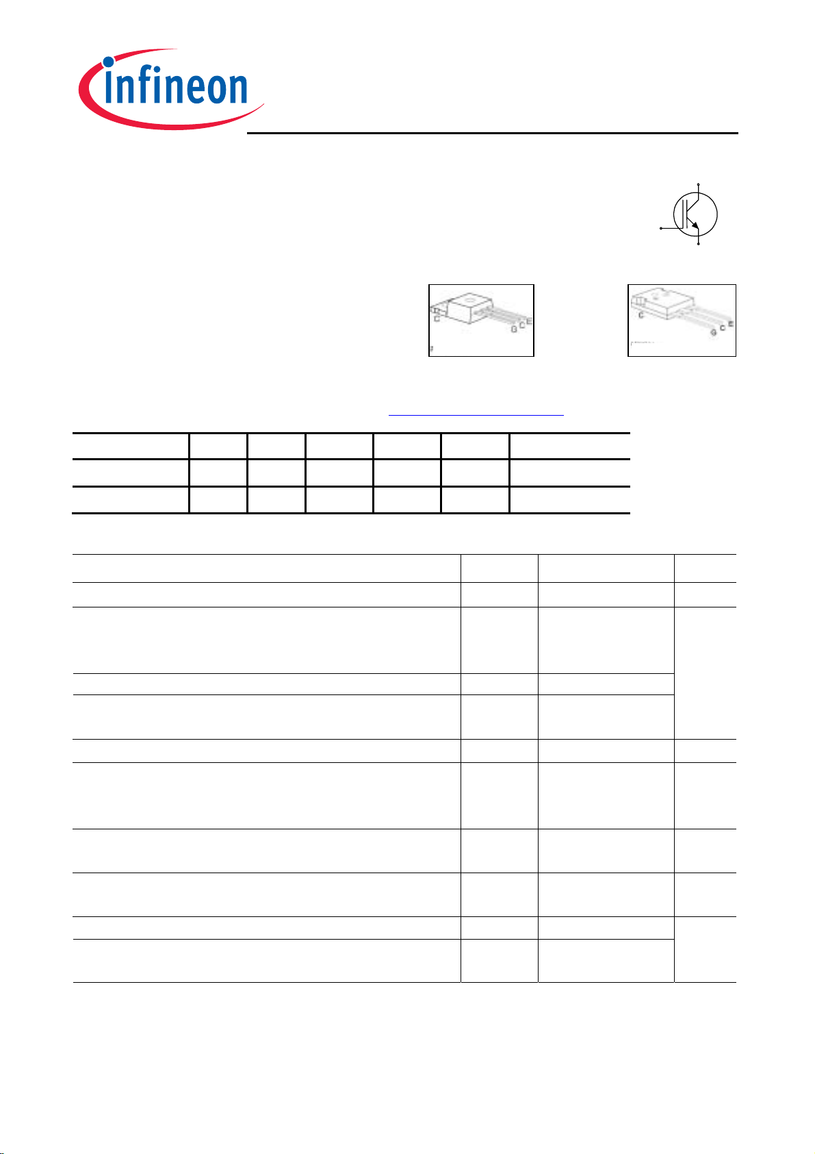
Fast IGBT in NPT-technology
• 75% lower E
compared to previous generation
off
combined with low conduction losses
• Short circuit withstand time – 10 µs
• Designed for:
- Motor controls
- Inverter
• NPT-Technology for 600V applications offers:
- very tight parameter distribution
- high ruggedness, temperature stable behaviour
- parallel switching capability
• Qualified according to JEDEC
1
for target applications
PG-TO-220-3-1
• Pb-free lead plating; RoHS compliant
• Complete product spectrum and PSpice Models : http://www.infineon.com/igbt/
Type
I
V
CE
V
C
Tj Marking Package
CE(sat)
C
G
E
PG-TO-247-3-21
SGP30N60 600V 30A 2.5V
SGW30N60 600V 30A 2.5V
150°C
150°C
G15N60 PG-TO-220-3-1
G15N60 PG-TO-247-3-21
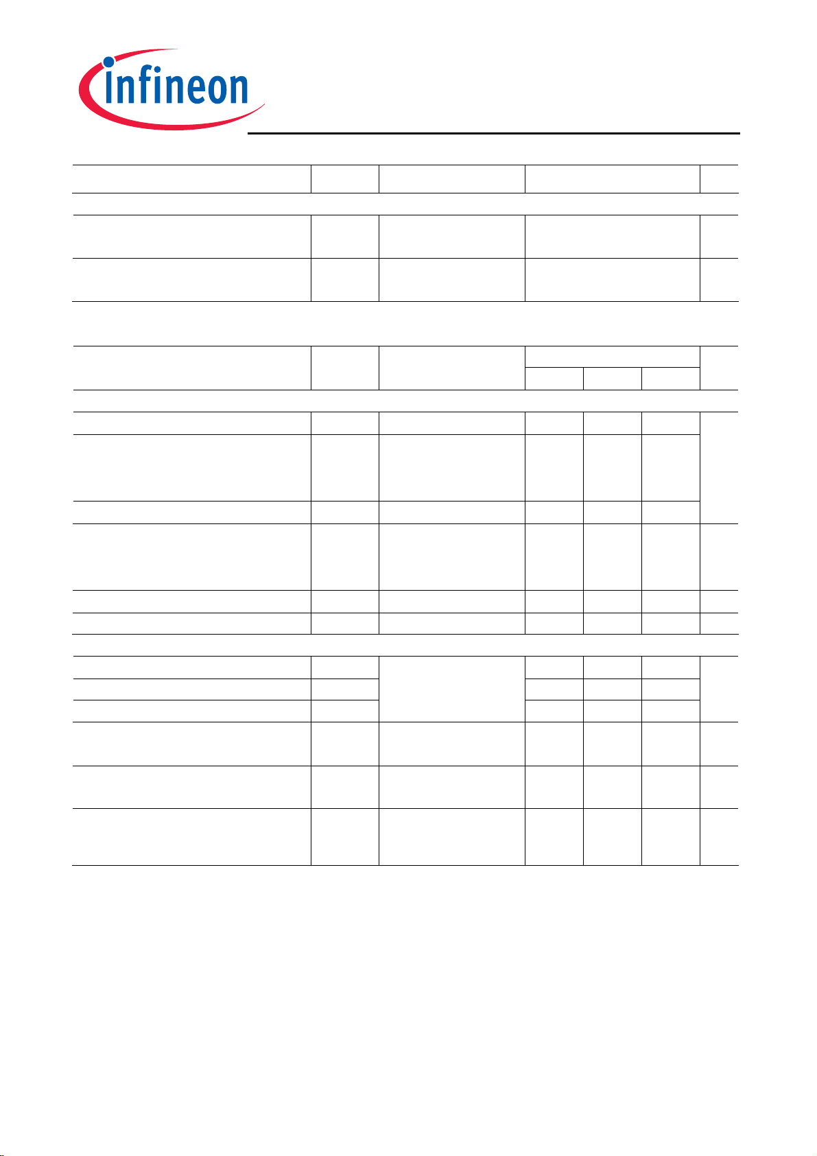
Maximum Ratings
Parameter Symbol Value Unit
Collector-emitter voltage
DC collector current
= 25°C
T
C
T
= 100°C
C
Pulsed collector current, tp limited by T
I
jmax
Turn off safe operating area
≤ 600V, Tj ≤ 150°C
V
CE
Gate-emitter voltage
Avalanche energy, single pulse
= 30 A, VCC = 50 V, R
I
C
start at T
= 25°C
j
= 25 Ω,
GE
Short circuit withstand time2
= 15V, V
V
GE
≤ 600V, Tj ≤ 150°C
CC
Power dissipation
= 25°C
T
C
Operating junction and storage temperature
Soldering temperature,
V
CE
I
C
Cpuls
-
V
GE
E
AS
t
SC
P
tot
T
j
T
s
, T
stg
600 V
41
A
30
112
112
±20
V
165 mJ
10
µs
250 W
-55...+150
°C
260
wavesoldering, 1.6mm (0.063 in.) from case for 10s
1
J-STD-020 and JESD-022
2
Allowed number of short circuits: <1000; time between short circuits: >1s.
1 Rev. 2.1 June 06

SGP30N60
SGW30N60
Thermal Resistance
Parameter Symbol Conditions Max. Value Unit
Characteristic
R
R
thJC
thJA
PG-TO-220-3-1
0.5 K/W
PG-TO-247-3-21
V
(BR)CES
V
CE(sat)
V
GE(th)
I
CES
I
GES
VCE=20V, IC=30A
g
fs
C
iss
C
oss
C
rss
Q
Gate
L
E
VGE=0V, I
=500µA
C
VGE = 15V, IC=30A
=25°C
T
j
T
=150°C
j
=700µA,V
I
C
VCE=600V,VGE=0V
T
=25°C
j
T
=150°C
j
VCE=0V,VGE=20V
V
=25V,
CE
V
=0V,
GE
f=1MHz
VCC=480V, IC=30A
V
=15V
GE
PG-TO-220-3-1
PG-TO-247-3-21
I
C(SC)
=15V,t
V
GE
≤ 600V,
V
CC
≤ 150°C
T
j
SC
CE=VGE
≤10µs
62
40
Value
Unit
min. Typ. max.
600 - -
1.7
-
2.1
2.5
2.4
3.0
V
3 4 5
-
-
-
-
40
3000
µA
- - 100 nA
- 20 - S
- 1600 1920
pF
- 150 180
- 92 110
- 140 182 nC
-
-
7
13
- nH
- 300 - A
IGBT thermal resistance,
junction – case
Thermal resistance,
junction – ambient
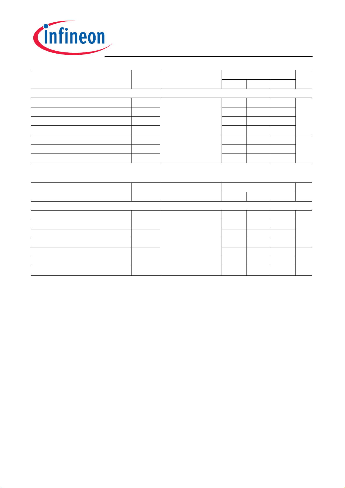
Electrical Characteristic, at T
= 25 °C, unless otherwise specified
j
Parameter Symbol Conditions
Static Characteristic
Collector-emitter breakdown voltage
Collector-emitter saturation voltage
Gate-emitter threshold voltage
Zero gate voltage collector current
Gate-emitter leakage current
Transconductance
Dynamic Characteristic
Input capacitance
Output capacitance
Reverse transfer capacitance
Gate charge
Internal emitter inductance
measured 5mm (0.197 in.) from case
Short circuit collector current2)
2)
Allowed number of short circuits: <1000; time between short circuits: >1s.
2 Rev. 2.1 June 06

SGP30N60
SGW30N60
Switching Characteristic, Inductive Load, at T
Parameter Symbol Conditions
IGBT Characteristic
Turn-on delay time
Rise time
Turn-off delay time
Fall time
Turn-on energy
Turn-off energy
Total switching energy
t
d(on)
t
r
t
d(off)
t
f
E
on
E
off
E
ts
Switching Characteristic, Inductive Load, at T
Parameter Symbol Conditions
IGBT Characteristic
Turn-on delay time
Rise time
Turn-off delay time
Fall time
Turn-on energy
Turn-off energy
Total switching energy
t
d(on)
t
r
t
d(off)
t
f
E
on
E
off
E
ts
=25 °C
j
=25°C,
T
j
=400V,IC=30A,
V
CC
V
=0/15V,
GE
=11Ω,
R
G
1)
L
=180nH,
σ
1)
C
=900pF
σ
Energy losses include
“tail” and diode
reverse recovery.
=150 °C
j
=150°C
T
j
=400V,IC=30A,
V
CC
V
=0/15V,
GE
= 11Ω,
R
G
1)
L
=180nH,
σ
1)
C
=900pF
σ
Energy losses include
“tail” and diode
reverse recovery.
Value
Unit
min. typ. max.
- 44 53
ns
- 34 40
- 291 349
- 58 70
- 0.64 0.77
mJ
- 0.65 0.85
- 1.29 1.62
Value
Unit
min. typ. max.
- 44 53
ns
- 34 40
- 324 389
- 67 80
- 0.98 1.18
mJ
- 0.92 1.19
- 1.90 2.38
1)
Leakage inductance L
an d Stray capacity Cσ due to dynamic test circuit in Figure E.
σ
3 Rev. 2.1 June 06

SGP30N60
SGW30N60
160A
t
=4µs
p
140A
I
c
100A
120A
100A
80A
TC=80°C
60A
, COLLECTOR CURRENT
40A
C
I
20A
0A
10Hz 100Hz 1kHz 10kHz 100kHz
TC=110°C
I
c
f, SWITCHING FREQUENCY
10A
, COLLECTOR CURRENT
C
I
0.1A
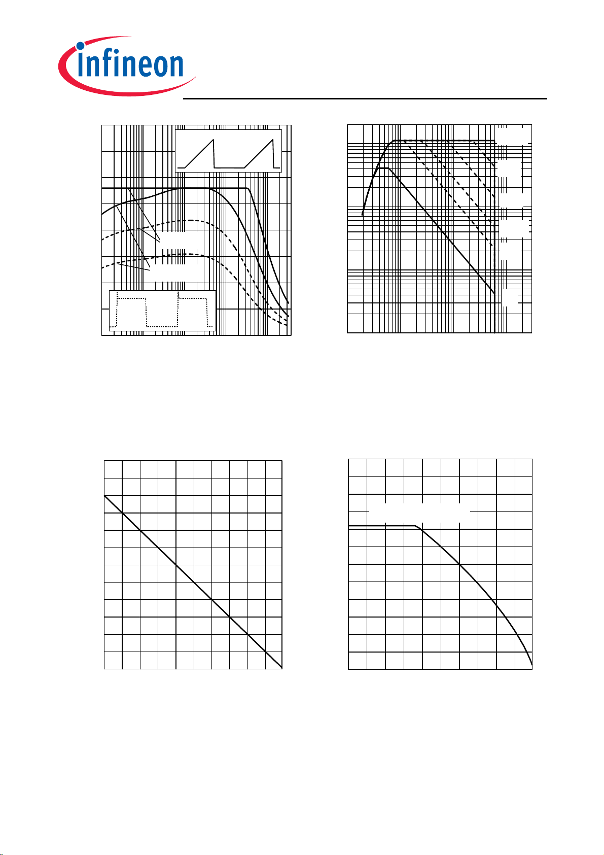
Figure 1. Collector current as a function of
switching frequency
(T
≤ 150°C, D = 0.5, V
j
V
= 0/+15V, R
GE
= 11Ω)
G
= 400V,
CE
300W
60A
1A
1V 10V 100V 1000V
VCE, COLLECTOR-EMITTER VOLTAGE
Figure 2. Safe operating area
(D = 0, T
= 25°C, Tj ≤ 150°C)
C
15µs
50µs
200µs
1ms
DC
250W
200W
150W
100W
, POWER DISSIPATION
tot
P
50W
0W
25°C 50°C 75°C 100°C 125°C
, CASE TEMPERATURE
T
C
Figure 3. Power dissipation as a function
of case temperature
≤ 150°C)
(T
j
50A
Limited by bond wire
40A
30A
20A
, COLLECTOR CURRENT
C
I
10A
0A
25°C 50°C 75°C 100°C 125°C
TC, CASE TEMPERATURE
Figure 4. Collector current as a function of
case temperature
(V
≤ 15V, Tj ≤ 150°C)
GE
4 Rev. 2.1 June 06
 Loading...