

Ω
SFH6943
Low Current Input
Mini Optocoupler
FEATURES
• Transistor Optocoupler in SOT223/10
Package
• End Stackable, 1.27 mm Spacing
• Low Current Input
• Very High CTR, 150% Typical at
V
=5 V
CE
I
=1 mA,
F
• Good CTR Linearity Versus Forward Current
• Minor CTR Degradation
• Field Effect Stable by TRIOS
(TRansparent IOn Shield)
• High Collector-Emitter Voltage,
V
CEO
=70 V
• Low Coupling Capacitance
• High Common Mode Transient Immunity
• Isolation Test Voltage: 1768 V
RMS
APPLICATIONS
• Telecommunication
• SMT
• PCMCIA
• Instrumentation
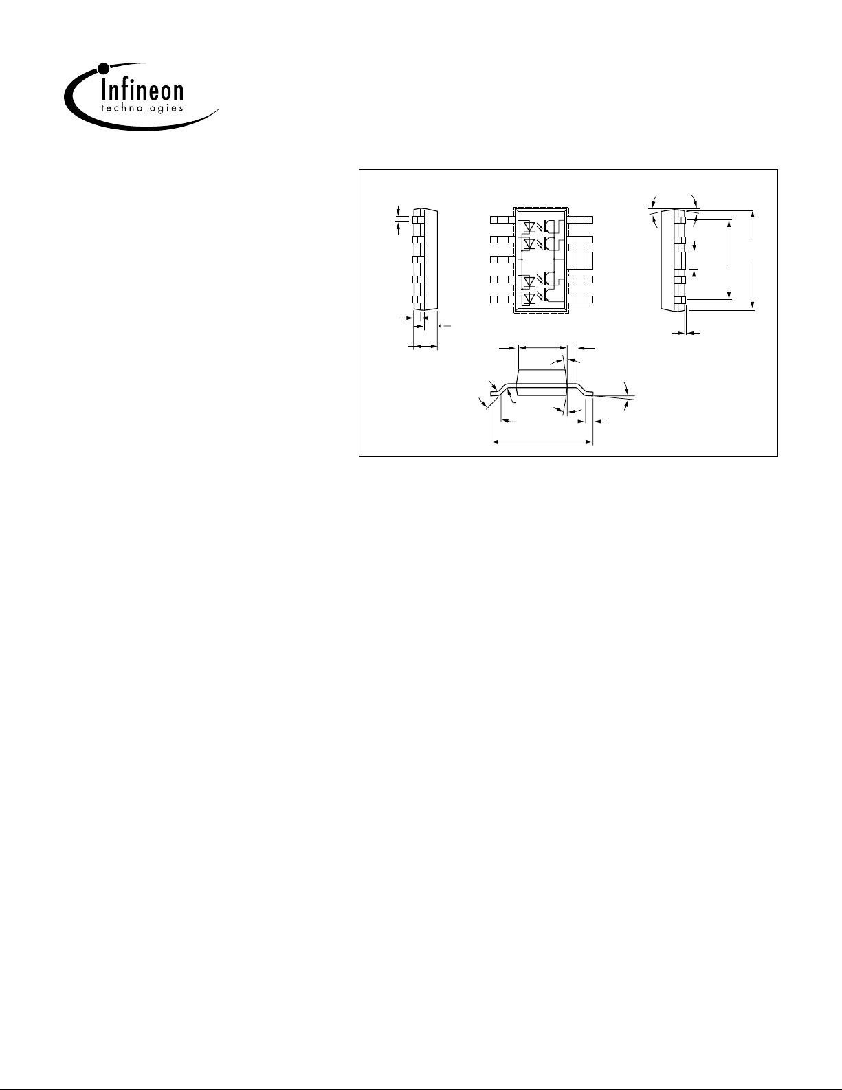
DESCRIPTION
The SFH6943 is a four channel mini-optocoupler
suitable for high density packaged PCB application. It has a minimum of 1768 V
isolation from
RMS
input to output. The device consists of four phototransistors as detectors. Each channel is individually controlled. The optocoupler is housed in
a SOT223/10 package. All the cathodes of the
input LEDs and all the collectors of the output
transistors are commoned enabling a pin count
reduction from 16 pins to 10 pins—a significant
space savings as compared to four channels that
are electrically isolated individually.
Dimensions in Inches (mm)
10°
7°
.016 (.41)
.018 (.46)
.063 ±.004
(1.60 ±.10)
Anode 1
Anode 2
Common 3
Cathode
Anode 4
Anode 5
.035
(.90)
0.004 (.10)
.01 (.25) R
max.
0.138 ±.004
(3.51 ±.10)
0.010 R
(.25)
45°
.276 ±.008
(7.01 ±.20)
10°
7°
10 Emitter 1
9 Emitter 2
8 Common
Collector
7 Emitter 3
6 Emitter 4
0.020 ±.004
(.51 ±.10)
0°–7°
0.020 (.51) min.
.043
(1.09)
.200 ±.005
(5.08 ±.13)
.002 +.002
–.001
(.05 +.05
–.03)
.256 ±.004
(6.50 ±.10)
Absolute Maximum Ratings
Emitter(GaAlAs)
Reverse Voltage . . . . . . . . . . . . . . . . . . . . . . . . . . . . . . . . . . . . . . . . . . . . .3 V
DC Forward Current . . . . . . . . . . . . . . . . . . . . . . . . . . . . . . . . . . . . . . . . 5 mA
Surge Forward Current (
tP≤
10 µs) . . . . . . . . . . . . . . . . . . . . . . . . . . . 100 mA
Total Power Dissipation. . . . . . . . . . . . . . . . . . . . . . . . . . . . . . . . . . . . .10 mW
Detector (Si Phototransistor)
Collector-Emitter Voltage. . . . . . . . . . . . . . . . . . . . . . . . . . . . . . . . . . . . . .70 V
Emitter-Collector Voltage. . . . . . . . . . . . . . . . . . . . . . . . . . . . . . . . . . . . . . .7 V
Collector Current. . . . . . . . . . . . . . . . . . . . . . . . . . . . . . . . . . . . . . . . . . 10 mA
Surge Collector Current (
t
<1 ms) . . . . . . . . . . . . . . . . . . . . . . . . . . . . 20 mA
P
Total Power Dissipation. . . . . . . . . . . . . . . . . . . . . . . . . . . . . . . . . . . . .20 mW
Package Insulation
Isolation Test Voltage (between emitter and detector,
refer to climate DIN 40046, part 2, Nov. 74), t=1 sec. . . . . . . . .1768 V
RMS
Creepage . . . . . . . . . . . . . . . . . . . . . . . . . . . . . . . . . . . . . . . . . . . . . . ≥4 mm
Clearance . . . . . . . . . . . . . . . . . . . . . . . . . . . . . . . . . . . . . . . . . . . . . . ≥4 mm
Comparative Tracking Index per DIN IEC 112/VDE0303, part 1 . . . . . . . 175
Isolation Resistance
V
=100 V,
IO
V
=100 V, T
IO
TA=25°C . . . . . . . . . . . . . . . . . . . . . . . . . . . . . . . . . . . ≥1011 Ω
=100 ° C . . . . . . . . . . . . . . . . . . . . . . . . . . . . . . . . . . ≥ 10
A
10
Storage Temperature Range. . . . . . . . . . . . . . . . . . . . . . . . . . .–55 to +150 ° C
Ambient Temperature Range . . . . . . . . . . . . . . . . . . . . . . . . . .–55 to +100 ° C
Junction Temperature . . . . . . . . . . . . . . . . . . . . . . . . . . . . . . . . . . . . . . 100°C
Soldering Temperature (t=10 sec. max.)
Dip soldering plus reflow soldering processes. . . . . . . . . . . . . . . . . 260°C
2000 Infineon Technologies Corp. • Optoelectronics Division • San Jose, CA
www.infineon.com/opto • 1-888-Infineon (1-888-463-4636)
OSRAM Opto Semiconductors GmbH & Co. OHG • Regensburg, Germany
www.osram-os.com • +49-941-202-7178 1 March 4, 2000-23
µ
3 µ s
Characteristics ( T
=25 ° C, unless otherwise specified)
A
Description Symbol Min. Typ. Max. Unit
Emitter (IR GaAs)
Forward Voltage,
Reverse Current,
Capacitance,
Thermal Resistance
I
=5 mA
F
V
=3 V
R
=0 V, f=1 MHz
V
R
V
I
C
R
F
R
0
thJA
— 1.25 — V
— 0.01 10
A
— 5 — pF
— 1000 — K/W
Detector (Si Phototransistor)
Collector-Emitter Voltage, I
Emitter-Collector Voltage, I
Capacitance,
V
=5 V, f=1 MHz
CE
Thermal Resistance
=10 µ A
CE
=10 µ A
EC
V
V
C
R
CEO
ECO
CE
thJA
70 ——V
7 ——V
— 6 — pF
— 500 — K/W
Package
Coupling Capacitance C
C
— 1 — pF
Description Symbol -2 -3 -4 Unit Condition
Coupling Transfer Ratio
Coupling Transfer Ratio
Collector-Emitter Leakage Current
E/
I
E/
I
CEO
I
F
I
F
63–200 100–320 160–500 %
typ, 100 ( ≥ 32) typ, 160 ( ≥ 50) typ, 250 ( ≥ 80) %
50 50 50 nA
I
=1 mA,
F
I
=0.5 mA,
F
V
=10 V
CE
I
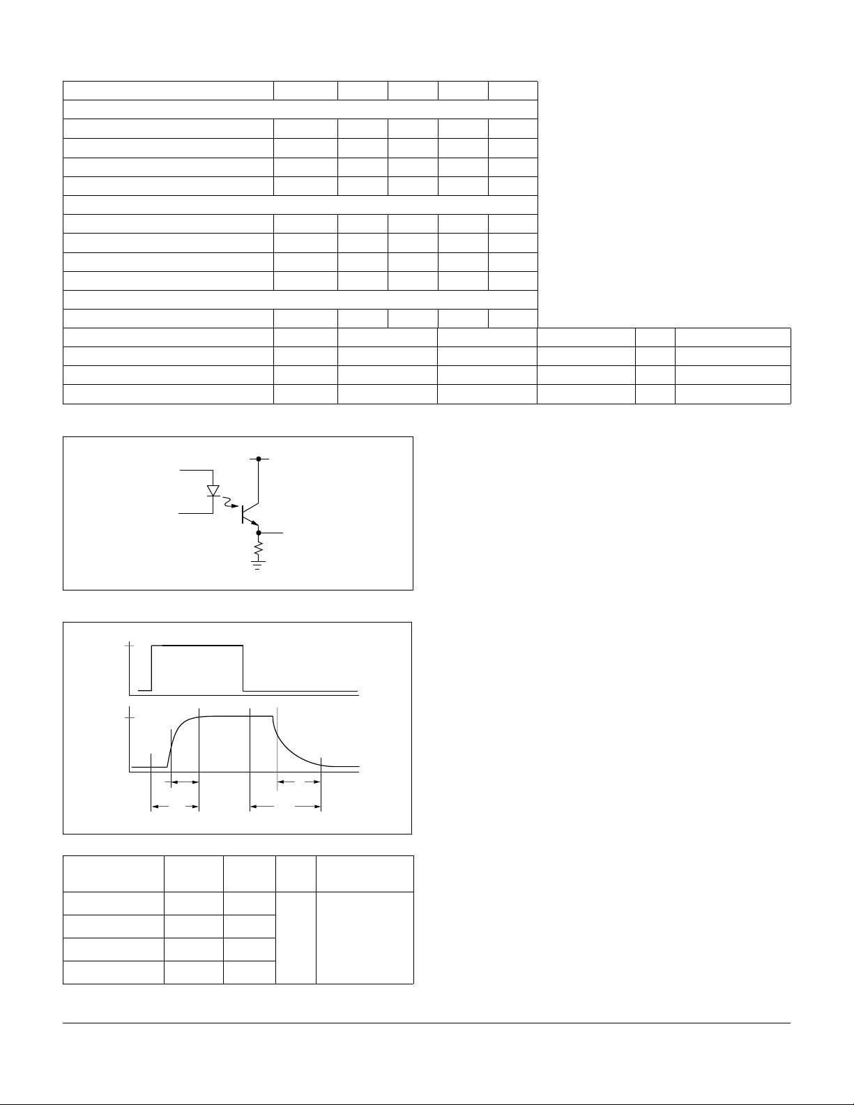
Figure 1. Switching times (non-saturated), typical
IF→
VCC=5 V
V
CE
V
CC
=1.5 V
=5 V
F=10 KHz
=50%
D
F
=2 mA
I
E
RE=100 Ω
↓
V
O
Figure 2. Switching waveform (non-saturated)
I
F
V
0
t
OFF
t
F
t
R
t
ON
Description Symbol Value Unit Test
Conditions
Turn-on Time
Rise Time
Turn-off Time
Fall Time
t
on
t
r
t
off
t
f
2.6
3.1
2.8
I
R
T
V
=2 mA
E
=100 Ω
E
=25 ° C
A
=5 V
CC
2000 Infineon Technologies Corp. • Optoelectronics Division • San Jose, CA SFH6943
www.infineon.com/opto • 1-888-Infineon (1-888-463-4636)
OSRAM Opto Semiconductors GmbH & Co. OHG • Regensburg, Germany
www.osram-os.com • +49-941-202-7178 2 March 4, 2000-23

)
)
)
Figure 3. LED current versus LED
voltage V
=f( I
F
F
1
10
0
10
/mA
F
I
–1
10
–2
10
.8 .9 1 1.1 1.2 1.3 1.4
VF/V
85°
50°
25°
–25°
Figure 4. Non-saturated current transfer
normalized to I
2.0
1.8
1.6
1.4
1.2
1.0
.8
NCTR
.6
.4
.2
0
10
=1 mA, NCTR=f( I
F
VCE=1.5V
T
=25°C
A
I
=1mA
F
–4
10–3 10
IF/A
F
–2
Figure 6. Collector-emitter leakage
current (typ.) I
I
=f( V
CEO
CE
3
10
2
10
1
10
0
10
/nA
–1
10
CEO
I
–2
10
–3
10
0 10 20 30 40 50 60 70
=0, T
F
V
/V
=25 ° C,
A
Figure 7. Permissible forward
current diode I
8
7
6
5
4
/mA
3
F
I
2
1
0
0 10 20 30 40 50 60 70 80 90 100
=f( T
F
TA/°C
=25 ° C )
A
Figure 9. T
ton,
tr,
10
3
t
off
=25 ° C, I
A
,
tt=f(
RL)
=1 mA,
F
VCC=5 V,
10
t
off
t
f
t
1
10
t/us
0
10
2
10
103 104 10
on
t
r
5
RL/OHM
Figure 10. Transistor output characteristics TA=25°C, ICE=1 (
VCE,
IF,)
Figure 5. Transistor capacitance
(typ.)
T
=25 ° C, f=1MHz, C
A
25.0
22.5
20.0
17.5
15.0
12.5
F
P
/
10.0
CE
C
7.5
5.0
2.5
0
10–2 10–1 100 101 10
2000 Infineon Technologies Corp. • Optoelectronics Division • San Jose, CA SFH6943
www.infineon.com/opto • 1-888-Infineon (1-888-463-4636)
OSRAM Opto Semiconductors GmbH & Co. OHG • Regensburg, Germany
www.osram-os.com • +49-941-202-7178 3 March 4, 2000-23
C
CE
VCE/V
CE
=f( V
CE
)
2
Figure 8. Permissible power
dissipation P
30
25
20
15
/mW
10
tot
P
5
0
0 10 20 30 40 50 60 70 80 90 100
tot
=f( T
TA/°C
)
A
Transistor
Diode
 Loading...