

Page 1

User Guide Please read the Important notice and the Safety precautions and the Warnings
www.infineon.com page 1 of 38 2021-01-29
UG-2020-28
User guide for REF-22K-GPD-INV-EASY3B
A reference design for a general purpose drive
About this document
Scope and purpose
This user guide provides an overview of the evaluation kit REF-22K-GPD-INV-EASY3B including its main
features, key data, pin assignments, mechanical dimensions and corresponding control card. The reference kit
REF-22K-GPD-INV-EASY3B is an industrial motor drive for three-phase 400 V AC grids and has a nominal power
of 22 kW.
The REF-22K-GPD-INV-EASY3B includes the Easy3B power module FP100R12W3T7_B11, the current sensor
TLI4971-A120T5, the gate driver IC 1ED3131MC12H, the 1.7 kV SiC-MOSFET IMBF170R1K0M1 and the
microcontrollers XMC4800-F144F2048 and XMC4300-F100K256. The combination of these Infineon products
allows the customer to evaluate these products in one design and experience the interaction between the
products.
Beside the hardware, the REF-22K-GPD-INV-EASY3B offers you software for control and communication. The
inverter can be controlled via a touch screen and PC-GUI.
Note: Please note that this product is not qualified according to the AEC Q100 or AEC Q101 documents of
the Automotive Electronics Council.
Intended audience
This user guide is intended for all technical specialists working on industrial drives and those interested in how
the latest Infineon products like IGBT7, XENSIV™ current sensors, EICE™ drivers and CoolSiC™ MOSFETs perform
under application conditions.
Reference Kit
The Infineon products are embedded on this PCB with functions and form factor close to a commercial design.
PCB and auxiliary circuits are optimized for the final design.
Note: Boards do not necessarily meet safety, EMI, quality standards (for example UL, CE) requirements.
Page 2

User Guide 2 of 38
2021-01-29
User Guide for REF-22K-GPD-INV-EASY3B
Reference design for motor general purpose drives
The reference board at a glance
Important notice
“Evaluation Boards and Reference Boards” shall mean products embedded on a printed circuit board
(PCB) for demonstration and/or evaluation purposes, which include, without limitation, demonstration,
reference and evaluation boards, kits and design (collectively referred to as “Reference Board”).
Environmental conditions have been considered in the design of the Evaluation Boards and Reference
Boards provided by Infineon Technologies. The design of the Evaluation Boards and Reference Boards
has been tested by Infineon Technologies only as described in this document. The design is not qualified
in terms of safety requirements, manufacturing and operation over the entire operating temperature
range or lifetime.
The Evaluation Boards and Reference Boards provided by Infineon Technologies are subject to functional
testing only under typical load conditions. Evaluation Boards and Reference Boards are not subject to the
same procedures as regular products regarding returned material analysis (RMA), process change
notification (PCN) and product discontinuation (PD).
Evaluation Boards and Reference Boards are not commercialized products, and are solely intended for
evaluation and testing purposes. In particular, they shall not be used for reliability testing or production.
The Evaluation Boards and Reference Boards may therefore not comply with CE or similar standards
(including but not limited to the EMC Directive 2004/EC/108 and the EMC Act) and may not fulfill other
requirements of the country in which they are operated by the customer. The customer shall ensure that
all Evaluation Boards and Reference Boards will be handled in a way which is compliant with the relevant
requirements and standards of the country in which they are operated.
The Evaluation Boards and Reference Boards as well as the information provided in this document are
addressed only to qualified and skilled technical staff, for laboratory usage, and shall be used and
managed according to the terms and conditions set forth in this document and in other related
documentation supplied with the respective Evaluation Board or Reference Board.
It is the responsibility of the customer’s technical departments to evaluate the suitability of the
Evaluation Boards and Reference Boards for the intended application, and to evaluate the completeness
and correctness of the information provided in this document with respect to such application.
The customer is obliged to ensure that the use of the Evaluation Boards and Reference Boards does not
cause any harm to persons or third party property.
The Evaluation Boards and Reference Boards and any information in this document is provided "as is"
and Infineon Technologies disclaims any warranties, express or implied, including but not limited to
warranties of non-infringement of third party rights and implied warranties of fitness for any purpose, or
for merchantability.
Infineon Technologies shall not be responsible for any damages resulting from the use of the Evaluation
Boards and Reference Boards and/or from any information provided in this document. The customer is
obliged to defend, indemnify and hold Infineon Technologies harmless from and against any claims or
damages arising out of or resulting from any use thereof.
Infineon Technologies reserves the right to modify this document and/or any information provided
herein at any time without further notice.
Page 3
User Guide 3 of 38
2021-01-29
User Guide for REF-22K-GPD-INV-EASY3B
Reference design for motor general purpose drives
The reference board at a glance
Safety precautions
Note: Please note the following warnings regarding the hazards associated with development systems.
Table 1 Safety precautions
Warning: The DC link potential of this board is up to 1000 VDC. When measuring
voltage waveforms by oscilloscope, high voltage differential probes must be used.
Failure to do so may result in personal injury or death.
Warning: The evaluation or reference board contains DC bus capacitors which take
time to discharge after removal of the main supply. Before working on the drive
system, wait five minutes for capacitors to discharge to safe voltage levels. Failure to
do so may result in personal injury or death. Darkened display LEDs are not an
indication that capacitors have discharged to safe voltage levels.
Warning: The evaluation or reference board is connected to the grid input during
testing. Hence, high-voltage differential probes must be used when measuring voltage
waveforms by oscilloscope. Failure to do so may result in personal injury or death.
Darkened display LEDs are not an indication that capacitors have discharged to safe
voltage levels.
Warning: Remove or disconnect power from the drive before you disconnect or
reconnect wires, or perform maintenance work. Wait five minutes after removing
power to discharge the bus capacitors. Do not attempt to service the drive until the bus
capacitors have discharged to zero. Failure to do so may result in personal injury or
death.
Caution: The heat sink and device surfaces of the evaluation or reference board may
become hot during testing. Hence, necessary precautions are required while handling
the board. Failure to comply may cause injury.
Caution: Only personnel familiar with the drive, power electronics and associated
machinery should plan, install, commission and subsequently service the system.
Failure to comply may result in personal injury and/or equipment damage.
Caution: The evaluation or reference board contains parts and assemblies sensitive to
electrostatic discharge (ESD). Electrostatic control precautions are required when
installing, testing, servicing or repairing the assembly. Component damage may result
if ESD control procedures are not followed. If you are not familiar with electrostatic
control procedures, refer to the applicable ESD protection handbooks and guidelines.
Caution: A drive that is incorrectly applied or installed can lead to component damage
or reduction in product lifetime. Wiring or application errors such as undersizing the
motor, supplying an incorrect or inadequate AC supply, or excessive ambient
temperatures may result in system malfunction.
Caution: The evaluation or reference board is shipped with packing materials that
need to be removed prior to installation. Failure to remove all packing materials that
are unnecessary for system installation may result in overheating or abnormal
operating conditions.
Page 4

User Guide 4 of 38
2021-01-29
User Guide for Ref_22k_GPD-INV_Easy3B
Reference design for motor general purpose drives
Table of contents
Table of contents
About this document ....................................................................................................................... 1
Important notice ............................................................................................................................ 2
Safety precautions .......................................................................................................................... 3
Table of contents ............................................................................................................................ 4
1 The reference board at a glance ............................................................................................... 5
1.1 Delivery content ...................................................................................................................................... 5
1.2 Block diagram .......................................................................................................................................... 5
1.3 Main features ........................................................................................................................................... 7
1.4 Board parameters and technical data .................................................................................................... 7
1.4.1 Overload profile normal duty ............................................................................................................ 8
1.4.2 Heavy duty overload profile .............................................................................................................. 9
2 System and functional description .......................................................................................... 10
2.1 Commissioning ...................................................................................................................................... 10
2.2 Description of the functional blocks ..................................................................................................... 14
2.2.1 Hardware partitioning ..................................................................................................................... 14
2.2.2 Isolation coordination ..................................................................................................................... 16
2.2.3 Board interconnection schemes ..................................................................................................... 17
2.2.4 Supply schemes ............................................................................................................................... 18
2.2.5 Component selection ....................................................................................................................... 18
3 System design....................................................................................................................... 19
3.1 Schematics ............................................................................................................................................ 19
3.2 Layout .................................................................................................................................................... 19
3.2.1 Power board ..................................................................................................................................... 19
3.3 Inverter cooling concept ....................................................................................................................... 21
3.4 Disassembly of the housing .................................................................................................................. 22
3.5 Bill of material ....................................................................................................................................... 25
3.6 Connector details .................................................................................................................................. 25
4 System performance ............................................................................................................. 28
4.1 Test results inverter start-up ................................................................................................................ 28
4.2 Operation under rated conditions ........................................................................................................ 29
4.3 Switching behavior of the IGBT turn-on ............................................................................................... 31
4.4 Switching behavior of the IGBT – turn-off ............................................................................................ 32
4.5 Thermal behavior of the inverter under high overload ....................................................................... 33
4.6 Short-circuit measurement ................................................................................................................... 34
5 References and appendices .................................................................................................... 36
5.1 Abbreviations and definitions ............................................................................................................... 36
5.2 References ............................................................................................................................................. 36
Revision history ............................................................................................................................. 37
Page 5
User Guide 5 of 38
2021-01-29
The reference board at a glance
User guide for REF-22K-GPD-INV-EASY3B
A reference design for a general purpose drive
1 The reference board at a glance
1.1 Delivery content
The reference kit is a general purpose drive developed for applications like pumps, fans, compressors,
conveyor belts. The design has the look and feel of a typical drive and includes EMI filter, pre-charge and
capacitor bank, isolated power supplies, power module, controls and heat sink with fan. It can be operated
directly on a three-phase grid, enabling a fast evaluation of Infineon's newest technologies like IGBT7, gate
driver, current sensor and control in one system. This enables the unique opportunity to see the improvement
by combining Infineon's newest technologies. You will see how the new IGBT7 modules work with the EICE™
gate driver, or test the accuracy of the current sensor.
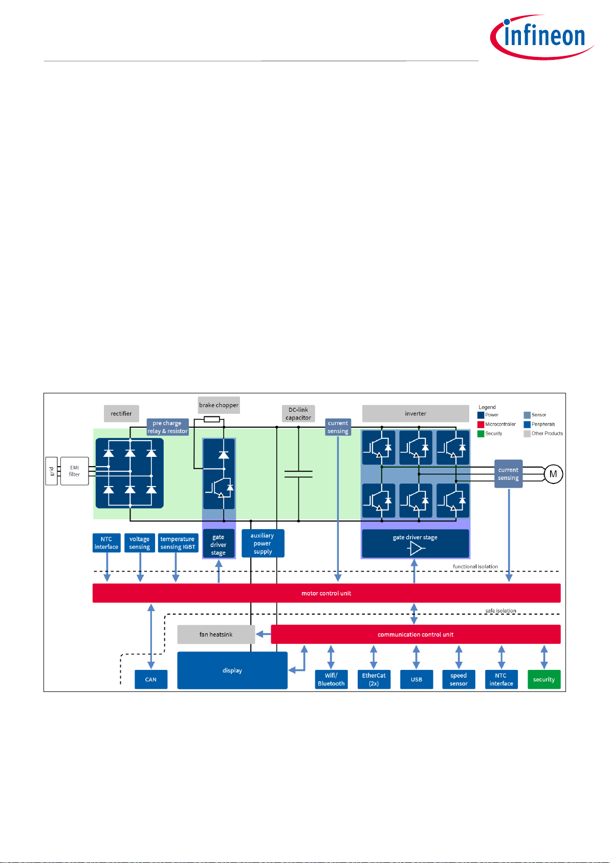
1.2 Block diagram
The block diagram of the inverter REF-22K-GPD-INV-EASY3B is shown in Figure 1. The board consists of five
boards: power board, EMI filter, high-voltage logic board, low-voltage interface board, and the DC-link board
which are mounted in one housing. For more details see Section 2.2.1.
Figure 1 Block diagram of the inverter
The reference kit REF-22K-GPD-INV-EASY3B is a fully operation industrial drive inverter which can be connected
to a three-phase AC input supply. The reference kit includes an input EMI-filter. The AC voltage is rectified via
the uncontrolled diode full bridge. The inrush current is limited by pre-charge circuitry. The rectified AC voltage
is stabilized by a DC-link capacitor bank. The IGBT six pack allows for the modulation of a three-phase output
voltage/current which can be varied in terms of its amplitude and frequency. This three-phase current is used
Page 6
User Guide 6 of 38
2021-01-29
The reference board at a glance
User guide for REF-22K-GPD-INV-EASY3B
A reference design for a general purpose drive
for controlling the speed and torque of the motor. During braking or deceleration of the motor, energy is
transferred back into the DC-link capacitor increasing the DC bus voltage. Therefore, a brake chopper is
included that absorbs this energy by switching an external brake resistor across the DC bus capacitors. The
three-phase input rectifier, the six pack as well as the brake chopper are all included in one power module, the
Easy3B IGBT FP100R12W3T7_B11. All IGBTs are switched using EICE™ drivers, the 1ED3131MC12H. The isolation
coordination details of the unit can be found in Section 2.2.2.
The current measurement of the three-phase output current is done with TLI4971-A120T5 current sensors. The
current signals are used for the motor control; additionally, these sensors are used to detect an external short
circuit for the IGBT’s. To protect the module against an internal short circuit, a fourth current sensor is
integrated between the DC-link capacitor and the IGBT module.
The auxiliary voltage for the inverter is generated with a DC/DC switch mode power supply (SMPS) converter.
The CoolSiC™-MOSFET IMBF170R1K0M1 is used in a flyback topology. More details about the flyback SMPS are
listed in Section 2.2.4.
The reference inverter uses two microcontrollers; one for control and one for communication. For control the
XMC4800-F144F2048 is used, for communication the XMC4300-F100K256 AA is designed in. Both
microcontrollers communicate via an UART interface. The communication microcontroller allows the inverter
to be controlled via a touch-screen or a PC-GUI. More details on the communication interface can be found in
Section 2.2.1.
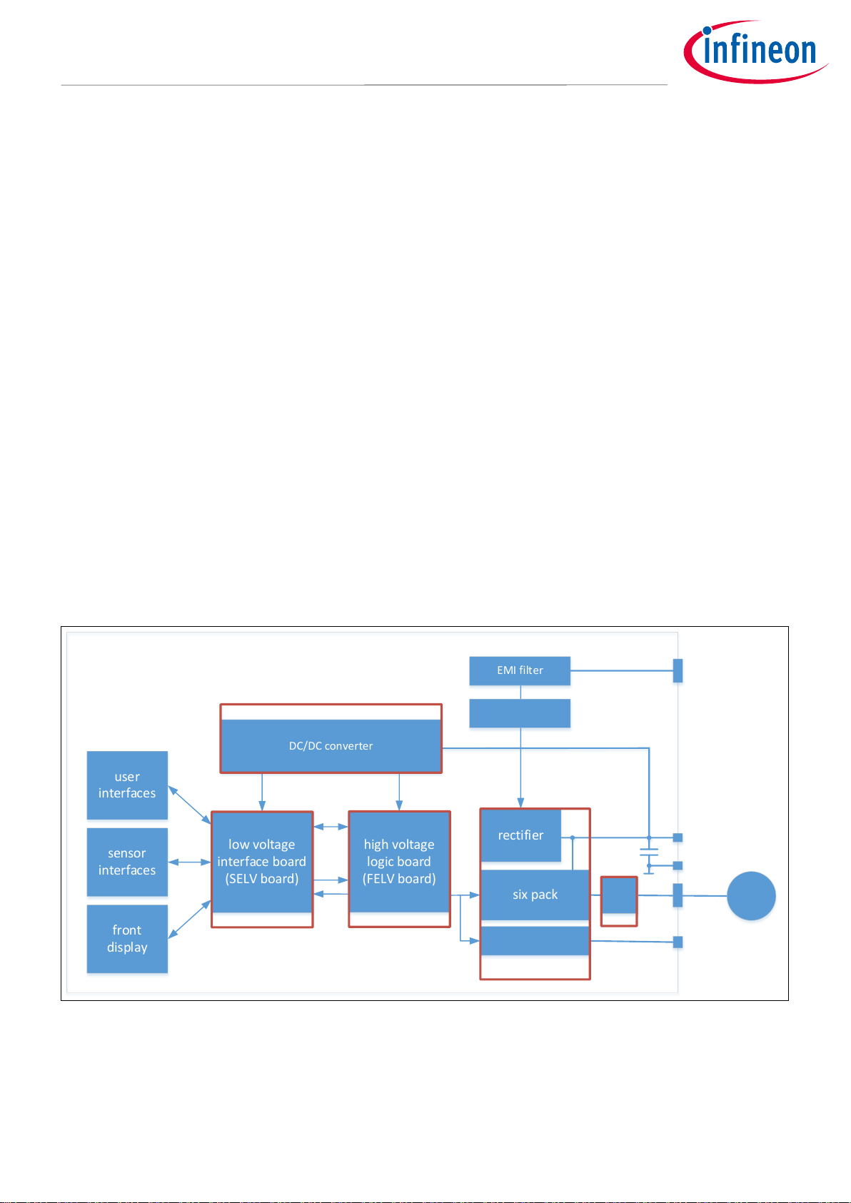
A simplified block diagram is shown in Figure 2. The block diagram shows the main components of the boards,
the DC/DC SMPS converter, the low-voltage interface board (SELV board), high-voltage logic board (FELV
board), the IGBT module incl. the gate driver IC, and the output phase current measurement. Also the main
Infineon components used in the specific blocks are listed in the diagram.
-_
high voltage
logic board
(FELV board)
low voltage
interface board
(SELV board)
rectifier
DC/DC converter
EMI filter
six pack
3Ph
Motor
user
interfaces
front
display
sensor
interfaces
3 phase
AC Input
3 phase
AC output
brake chopper
DC-Link
brake resistor
pre charge
resistor/relay
FP100R12W3T7_B11
1ED3131MC12H
curr
3 ph
TLI4971
IMBF170R1K0M1
XMC4800
XMC4300
Figure 2 Simplified block diagram of the inverter
Page 7

User Guide 7 of 38
2021-01-29
The reference board at a glance
User guide for REF-22K-GPD-INV-EASY3B
A reference design for a general purpose drive
1.3 Main features
FP100R12W3T7_B11: EASY3B IGBT7 module for high-current and high-power density [3]
TLI4971-A120T5: XENSIV
TM
current sensor for measuring high currents with minimal power loss [4]
1ED3131MC12H: Gate driver for optimal EMI performance and reduced power losses [5]
IMBF170R1K0M1: Infineon CoolSiC
TM
MOSFET 1700 V enables direct drive by most flyback controllers [6]
XMC4800-F144F2048 and XMC4300-F100K256 AA: XMC microcontrollers for inverter control and
communication [7]
1.4 Board parameters and technical data
The key parameters of the REF-22K-GPD-INV-EASY3B are shown in Table 2.
Table 2 Parameters of REF-22K-GPD-INV-EASY3B
Parameter
Symbol
Conditions
Value
Unit
Input line voltage
Vin
Three-phase AC ± 10%
380 … 480
V
Input frequency
fin
± 3 Hz
50 … 60
Hz
Output voltage
V
out
three-phase AC
0 V … 0.95 x input voltage
V
Output frequency
f
out
0 … 550
Hz
Switching frequency of
motor output
fsw
Factory setting 4 kHz
4
kHz
Rated power
P
rated
22
kW
Rated current
I
rated
45
A
Low overload - base
load power
PLO
T
amb
<= 35°C
22
kW
Low overload - base
load current
ILO 45
A
High overload - base
load power
PHO 18.5
kW
High overload - base
load current
IHO 38
A
Power losses
P
loss
< 700
W
Weight
m
inv
< 10
kg
Ambient temperature
T
amb
Relative humidity RH; 30% <
RH< 80%
10 to 35
°C
Page 8
User Guide 8 of 38
2021-01-29
The reference board at a glance
User guide for REF-22K-GPD-INV-EASY3B
A reference design for a general purpose drive
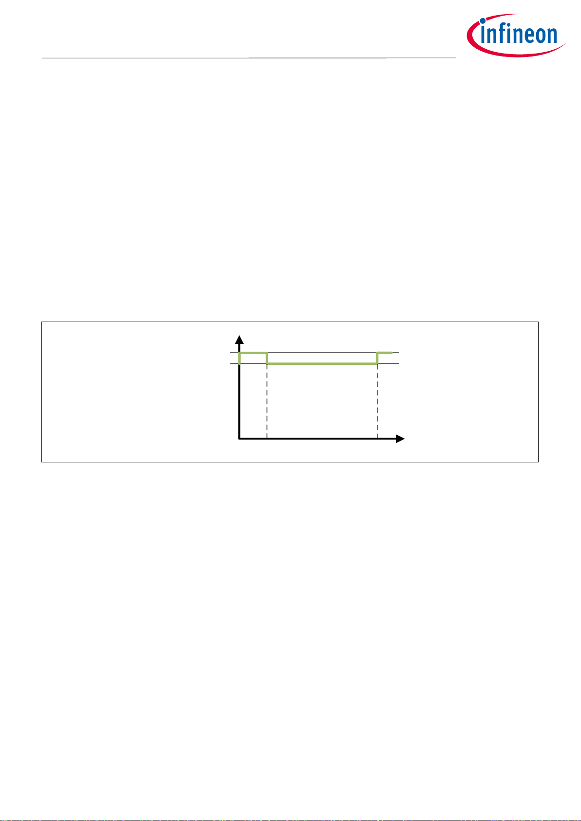
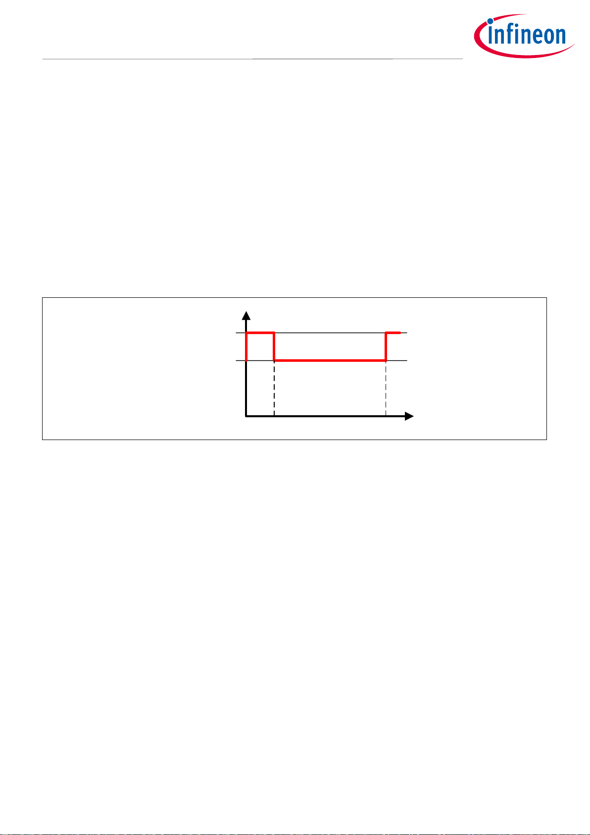
1.4.1 Overload profile normal duty
The normal duty (ND) load cycle assumes a uniform base load with low requirements during short acceleration
times at high torque; see Figure 3. Typical applications when designing according to normal duty include:
- Pumps, fans and compressors
- Wet or dry blasting technology
- Mills, mixers, kneaders, crushers, agitators
- Basic spindles
- Rotary kilns
- Extruders
Typical converter load cycle:
110% I
LO
= 50 A
60
300
time in s
100% of I
LO
= 45 A
current
in A
Figure 3 Overload profile normal duty
Page 9
User Guide 9 of 38
2021-01-29
The reference board at a glance
User guide for REF-22K-GPD-INV-EASY3B
A reference design for a general purpose drive
1.4.2 Heavy duty overload profile
The heavy duty (HD) load cycle permits dynamic accelerating phases at a reduced base load; see Figure 4.
Typical applications when designing according to heavy duty include:
- Horizontal and vertical conveyor technology (conveyor belts, roller conveyors, chain conveyors)
- Centrifuges
- Escalators/moving stairways
- Lifters
- Elevators
- Gantry cranes
- Storage and retrieval machines
Typical converter load cycle:
150% of I
HO
= 57 A
60
300
100% of I
HO
= 38 A
time in s
Figure 4 Overload profile heavy duty
Page 10
User Guide 10 of 38
2021-01-29
System and functional description
User guide for REF-22K-GPD-INV-EASY3B
A reference design for a general purpose drive
2 System and functional description
2.1 Commissioning
The REF-22K-GPD-INV-EASY3B must be connected to a TN-S line system as shown in Figure 5. The connections
to the inverter can be made only after the converter is unpacked and all packaging material has been removed.
Ref_22k_GPD-INV_Easy3B
Transformer
or generator
L1
L2
L3
N
PE
Figure 5 Connection of the inverter to TN-S line system
A TN-S system transfers the PE protective conductor to the installed plant or system using a cable. Generally, in
a TN-S system, the neutral point is grounded. A TN system can transfer the neutral conductor N and the PE
protective conductor either separately or combined. Also the connection to a TT system is permissible, but the
connection to an IT is not permissible. The reason here is the missing or high-impedance earth connection.
The connection of the inverter is shown in Figure 6. The cross-section of the wires for the line connection, the
brake chopper and the motor cable are in the range of 1.5 to 10 mm². Ensure that the inverter is in a no-voltage
condition and the DC-link is discharged.
Page 11
User Guide 11 of 38
2021-01-29
System and functional description
User guide for REF-22K-GPD-INV-EASY3B
A reference design for a general purpose drive
To connect the line feeder cables (L1, L2, L3 and PE), see Figure 6. To ensure correct fusing, it is recommended
to make a selection according to IEC is 3NA3824 (80A). Also, connect the motor feeder cables (PE, U, V and W) to
the inverter. The connection of a brake resistor is optional.
L1
L2
L3
PE
PE
U
V
W
R
brake
Figure 6 Connecting of the inverter
Also connect a USB cable to the inverter allowing for communication with the drive. The USB port is located at
the front of the inverter; see Figure 7.
Figure 7 USB port of the inverter
Page 12
User Guide 12 of 38
2021-01-29
System and functional description
User guide for REF-22K-GPD-INV-EASY3B
A reference design for a general purpose drive
Before you start the inverter, you need to install the XMC driver and launch the GUI. The software can be
downloaded via Infineon.com. Please register your inverter to get access to the software.
For installation, it is required to have admin rights on your computer. The software was tested with a laptop
(HP EliteBook 840 G5) and Windows 10 Enterprise (Build: 10.0.17134). You have to first install the USB driver, so
extract the file XMC_WinUSBDriver.zip.
To start with the installation, connect your computer with a USB cable to the inverter, and apply an appropriate
voltage to the line feeder cable. The inverter will start operation in idle mode. Now you can install the USB
driver: Go to “Control Panel\All Control Panel Items” then to “Device Manager.” Select the new USB device
“Infineon WinUSB Device;” see Figure 8 part 1, and double click it.
Figure 8 USB device installation
The window, as shown in Figure 8 part 2, will then appear. Click on the “Driver” tab, then “Update Driver” as
shown in Figure 8 part 3. Now select the extracted folder “XMC_WinUSBDriver” as shown in Figure 8 part 4. Click
on “OK” and close all windows you opened previously. The USB driver is now installed.
Page 13

User Guide 13 of 38
2021-01-29
System and functional description
User guide for REF-22K-GPD-INV-EASY3B
A reference design for a general purpose drive
The next step is to extract the file GUI_20200819.zip; the software is available at Infineon.com. Open the folder
“Debug” and double click on “GPD Inverter.exe”. A window as shown in Figure 9 (left side) appears. You can
connect your drive system by selecting the USB device via the drop-down menu and click on “Connect.” Now
your computer is communicating with the drive system.
Figure 9 Main GUI and Config tab
Be clicking on the “Config” tab, a window will be shown as in Figure 9 (right side). You can read the Config file
from your inverter by clicking on “Read config.” Now you can change the settings. The “Control Method” can be
selected either as “V/f” or “Manual.” The parameters for the “V/f” mode can be adjusted in the “Inverter
Configuration” window. In the manual mode, you can select the “Speed” value and the “Amplitude” value
manually; see the “General” Tab of the GUI. In the “Config” tab you can also change the “IGBT Overtemp
shutdown” value. The “Load Pulse Pattern Config” window allows you to operate the inverter in a periodic or
cyclical mode. This function works only in “Manual” mode, and changes the duty-cycle value for a specific time.
This approach allows for an easy implementation of an overload pattern, as shown in Figure 3 using an
inductive-resistive load. In addition, a short-circuit test is also possible via the GUI; further details will be
explained in Section 4.6.
Via the “General” tab, you can start the motor. You can run the motor in “V/f” mode; see section “Control
Method.” The speed of the motor, hence the output frequency of the inverter, can be adapted by the slider
“Speed.” After selecting your speed, click on “Update.” You can change the “V/f” ration in the “Config” tab, as
already mentioned. Via the “Manual” control mode, you can select the “Speed” and the “Amplitude” which
represents the modulation index.
Page 14

User Guide 14 of 38
2021-01-29
System and functional description
User guide for REF-22K-GPD-INV-EASY3B
A reference design for a general purpose drive
The current status of the inverter can be seen by clicking on “Diagnostics.” A window will appear as shown in
Figure 10 (left side). The voltage levels of the different power supplies will be shown, as well as any flagged
faults in the inverter.
Figure 10 Diagnostics and oscilloscope of the GUI
An additional feature of the inverter GUI is the oscilloscope function, which is shown in Figure 10 (right side).
The oscilloscope allows the measurement signals of the inverter to be shown, e.g. the phase output current, the
DC-link voltage or the NTC-temperature of the IGBT module.
2.2 Description of the functional blocks
2.2.1 Hardware partitioning
The inverter hardware is partitioned into five boards:
- Power board
- EMI filter
- High-voltage logic board
- Low-voltage interface board
- DC-link board
Thanks to the separation of these individual functions, a high level of functionality can be implemented with
minimum board space. Each board will be described in the following:
Power board:
The power board is used as a central connection and wiring unit between all other sub-boards. It contains the
main connectors (power inlet and outlet), the power module, the main DCDC-converter and the gate driver
including their power supplies. While the power board itself only contains a small DC-link capacitor, it connects
to the capacitor bank which has ix (3 sets of 2 in series) electrolytic capacitors.
DC-link board:
The board has the electrolytic capacitors of the inverter. The separation of the capacitors on an additional
board allows more design freedom and a more compact design of the inverter.
Page 15

User Guide 15 of 38
2021-01-29
System and functional description
User guide for REF-22K-GPD-INV-EASY3B
A reference design for a general purpose drive
EMI-Filter:
The EMI input filter is used to suppress RF noise generated by the inverter operation. It is designed as threephase CLC-topology. Due to the size and weight of the individual components, it is implemented on a separate
sub-board that connects to the power board via solder connectors.
High-voltage logic board (FELV board):
All logic functions required to control the drive motor are implemented on the high-voltage (HV) logic board. It
is based on a XMC4800 microcontroller as its central processing unit. The board contains the infrastructure to
supply and supervise the microcontroller, diagnostic functions for the high-voltage part of the drive as well as
all safety and protection functions needed to protect the inverter in case of overload or short-circuit conditions.
The HV board features a direct connection the components on the power board. All control inputs for the motor
control as well as the diagnostic status information are provided via a UART link to the low-voltage (SELV)
interface board. Besides the UART link, the board features both a digital status input and output signal to
indicate and receive information on critical error or fault conditions.
In order to minimize the number of required isolation barriers, the FELV board is referenced to the negative
potential of the DC-link.
Low-voltage logic board (SELV board):
The low-voltage logic board is used to provide the user and external sensor interface functions. It features
connectivity options for:
- EtherCat
- USB 2.0
- WLAN
- Bluetooth
- RS485
- High-Speed CAN
Besides the user interface function, the board also provides the capability to interface with external sensors,
such as:
- High-resolution rotor speed sensor (two wire current interface)
- High-resolution rotor angle sensor (GP-HSSI Interface)
- Temperature sensor
Besides the connectivity options to remote control units, the SELV board can also be connected to a local touch
pad display. This local control input allows the display of current operating conditions as well as basic user
control.
The data exchange between SELV and FELV board is established via a bidirectional UART link. All relevant
control commands received via the above-listed interface options or the touch display are forwarded to the
FELV board via this link. For safety and redundancy reasons, the board provides two additional direct
connections to the FELV board (1x input, 1x output) for error indication on the respective board. In case of a
broken UART connection, critical error conditions on either board can be indicated via these redundant signals
to cause the inverter to transition into a safe state.
Page 16

User Guide 16 of 38
2021-01-29
System and functional description
User guide for REF-22K-GPD-INV-EASY3B
A reference design for a general purpose drive
In order to simplify the supply scheme for the multiple external user interfaces, the SELV board is supplied via a
safety-isolated, low-voltage power supply. The connection to the high voltage logic board (UART, direct
connection lines) is therefore established via digital isolator devices featuring reinforced isolation capability.
2.2.2 Isolation coordination
The inverter design provides three major main voltage domains:
- A mains-connected domain
- A low-voltage domain with functional isolation
- A safety-isolation domain
In Figure 11 you will find a drawing of the basic isolation coordination scheme.
Figure 11 Basic isolation coordination scheme, the low- voltage interface board is referenced to PE
and the high- voltage logic board is referenced to DC-
All power components (EMI filter, rectifier, IGBT inverter, brake switch) are directly connected to the mains
supply domain. The main controller is based on a functional isolated scheme, which is connected to the DCpotential of the power domain. Thanks to this isolation scheme, all interfaces between the power domain and
the main control domain only provide functional isolation. This applies in particular for the gate drivers, their
power supply, the output current sensors and the voltage measurement circuits. All user interface connections
are implemented on a safety-insulated domain. In order to establish a communication link between the safetyisolation domain and the functional isolation domain, a digital interface using a safety isolated data coupler is
Page 17

User Guide 17 of 38
2021-01-29
System and functional description
User guide for REF-22K-GPD-INV-EASY3B
A reference design for a general purpose drive
implemented. The supply for the entire board is provided by a centralized DC/DC converter which takes power
from the mains supplied DC-link. The converter provides two output voltages, a functional isolated output for
the functional isolation domain (FELV) and a reinforced output voltage for the user interface (SELV) domain.
2.2.3 Board interconnection schemes
The power board is used as a main platform for all sub-boards. The mains power connection is performed by
power connectors on the bottom-left side of the inverter board. After passing the EMI filter board, which is
connected to the left side of the power PCB, the power is routed to the power module. The rectification of the
AC input power is performed in the power module; the DC-link capacitors are located on the right side of the
inverter and are connected via the power PCB. Since the capacitor bank is implemented as a separate unit, the
mechanical and electrical connections are made by special mounting screws. A CAD-model of the inverter is
shown in Figure 12.
Figure 12 Inverter Construction Scheme (front-left view), Housing removed
The inverter power supply is performed by a DC/DC converter which generates galvanically isolated supply
voltages for the power board, the high-voltage control board and the user interface board; see Figure 13. Both
user interface boards as well as the high-voltage control board are connected the power board via pin headers.
The user interface board connects to the power board on a safety-isolation island which provides the DC power
for the board and the isolation stage for the digital communication link to the high-voltage control board.
Connections to external sensors (e.g. rotor position sensor) or external communication buses (EtherCAT, USB,
RS485, CAN) are directly provided by the user interface board. All gate-driver control signals as well as all
voltage and current measurement signals are routed to the high-voltage control board via high pin-count
connectors.
High Voltage Control Board (FELV)
User Interface Board (SELV)
Power Board
EMI Filter
Board
Mains Supply Input
Power Output
Page 18

User Guide 18 of 38
2021-01-29
System and functional description
User guide for REF-22K-GPD-INV-EASY3B
A reference design for a general purpose drive
Figure 13 Inverter Construction Scheme (top-right view), Housing removed
2.2.4 Supply schemes
The three-phase AC input voltage is rectified to the DC-link supply voltage by the B6 rectifier bridge in the
power module. In order to prevent high inrush currents during power-up when the three-phase supply is first
connected, the DC-link capacitors are pre-charged via power resistors. After the capacitors are charged to
match the line voltage, the power resistors are shorted out using power relays.
The DC-link voltage is converted to two low-voltage domains by a SiC-based flyback converter. A first output
voltage (V15_HV) is used as the low-voltage supply for the functional isolated part of the inverter, supplying the
gate drivers and the high-voltage logic board. The second voltage domain (V24_SELV ) is used to power the lowvoltage user interface board, local sensors (e.g. heat sink temperature sensor) and the cooling fans.
2.2.5 Component selection
The power module is in an EASY 3B package, part number FP100R12W3T7_B11, based on the latest IGBT7
technology allowing a compact and economic solution for an industrial drive. The FP100R12W3T7_B11 module
carries all power semiconductors which are needed to control the motor current [1]. Due to the reduced VCEsat
voltage compared to IGBT4 and enhanced switching controllability, the IGBT7 technology is tailored for
industrial drives. For short-circuit protection of the IGBTs and for motor current control, the current sensor
TLI4971-A120T5 is used. The TLI4971-A120T5 provides a fast short-circuit detection time and accurate
measurement results over a wide temperature range [2]. For the gate driver IC, the EICE™ driver 1ED3131MC12H
was selected. It is a single-channel isolated IGBT gate driver IC with a source and sink capability of 3 A.
The Infineon CoolSiCTM MOSFET IMBF170R1K0M1 with a blocking capability of 1700 V is used for the auxiliary
power supply. By using the SiC-MOSFET, the design of the flyback inverter can be simplified.
The reference inverter uses two microcontrollers; one for control and one for communication. For control, the
XMC4800-F144F2048 is used, for communication, the XMC4300-F100K256 AA is designed in. Both
microcontrollers communicate via a UART interface.
DC-Link Capacitors
DC/DC Converter
Page 19

User Guide 19 of 38
2021-01-29
System design
User guide for REF-22K-GPD-INV-EASY3B
A reference design for a general purpose drive
3 System design
3.1 Schematics
The schematics of the design are available via Infineon.com. Keep in mind that the inverter consists of five
boards, hence you will find one schematic for each board.
Table 3 Schematic overview
Board name
File name in zip folder
Power board
22kW_Inverter_Power_Board_v1.3_2021-01-11.pdf
DC-link board
U109_GPD_DCLinkCaps_v1.0_2019-10-23.pdf
EMI filter
U109_22kWGPD_EMI-filter_v2.1_2020-12-02.pdf
High voltage logic board
22kW_Inverter_Logic_v1.2_2020-09-01.pdf
Low voltage interface
22kW_Inverter_Interfaces_v1.2_2020-12-02.pdf
Connection between high
voltage logic board and low
voltage Interface
U109_GPD_FlexPCBConnector_v1.0_2020-12-02.pdf
Isolation sheet between
power board and heat sink
U109_GPD_HeatsinkIsolation_v1.0_2020-12-02.pdf
Gasket to separate clean
and dirty air
U109_GPD_Sealing_v1.0_2020-12-02.pdf
The Altium™ project files are available on request.
3.2 Layout
3.2.1 Power board
The layout of the power board is shown in Figure 14; in Table 4 you will find the names of each block.
The AC input connector (1), AC output connector (2), the brake resistor connector (3) as well as the DC-link
connections (4) are located on the left hand side of the power board. The EMC filter is connected to the board in
the area marked (5). The high-side gate drivers are located in the area marked (6) and the low-side gate driver
are marked in section (12).
The interface to the high-voltage logic board (FELV board) is marked (7); this board has the interface
connectors. The output phase current measurement is marked (8); all three-phase currents are measured, also
the current between the DC-link capacitor and IGBT module is measured.
The IGBT module will be pressed in the area marked (9). The auxiliary power supply is located in the area
marked (10), the SiC MOSFET is soldered to the PCB in the area (11). The DC-link board is screwed to the power
board in the area marked (12).
The interface to the low-voltage interface board (SELV board) is marked (13). The safe isolation communication
between the high-voltage logic board (FELV board) and low-voltage interface board (SELV board) is realized
with the IC located on the PCB in area (14). The position of the pre-charge relay is shown at (16) and the precharge resistors are shown at (17).
Page 20

User Guide 20 of 38
2021-01-29
System design
User guide for REF-22K-GPD-INV-EASY3B
A reference design for a general purpose drive
Figure 14 Layout of the power board
Table 4 Functional block - power board layout
Block number
Function
1
AC input connector
2
AC output connector
3
Brake resistor connector
4
DC-link connector
5
EMI-filter connections
6
High-side gate driver with gate driver IC 1ED3131MC12H
7
Connector for motor control board
8
Output phase current sensor measurement with TLI4971-A120T5
9
IGBT module with IGBT7 - FP100R12W3T7_B11
10
Auxiliary power supply
11
CoolSiCTM MOSFET IMBF170R1K0M1 of the auxiliary power supply
12
Low-side gate driver with gate driver IC 1ED3131MC12H
13
Connector for communication interface board
14
Isolation barrier for communication between high-voltage logic board (FELV board) and low
voltage interface board (SELV board)
15
DC-link current sensor TLI4971-A120T5
16
Pre-charge relay
17
Pre-charge resistors
18
DC-Link
Page 21

User Guide 21 of 38
2021-01-29
System design
User guide for REF-22K-GPD-INV-EASY3B
A reference design for a general purpose drive
The gate layout of the high-side IGBT of the phase U is shown as an example in Figure 15. The traces of the
emitter and gate trace are on top of each other, which minimizes any parasitic inductances.
gate
emitter
minimize the stray
inductance by overlaying
gate and emitter trace
Figure 15 Gate layout of the high-side IGBT of phase U
3.3 Inverter cooling concept
A three-channel cooling system provides the cooling of the inverter, as seen in Figure 1 and Figure 16.
The main cooling of the IGBT is done by a heat sink and an integrated 92 mm fan with a temperature controlled
flowrate of 0-270 m³/h. The air is drawn in the bottom of the unit and blown up through the heat sink to the
outlet at the top of the enclosure, assuming a normal wall mounting position.
A 52 mm auxiliary fan cools the DC-link capacitors and operates at a constant speed with a flow rate of 20m³/h.
As shown in Figure 16 the air is blown into an air channel at the bottom of the capacitor array. To provide an
improved cooling over the entire surface of each capacitor the air is directed up one side and then channeled
via small slits between each capacitor and then finally along the side of the heat sink to the air outlet at the top
of the enclosure.
A second 52 mm fan, also operating at a constant speed, cools a third channel containing the EMI filter. The air
flows beside the heat sink and over the indictors and capacitors of the EMI filter. This cooling channel has a
separate air outlet at the top of the enclosure.
Page 22

User Guide 22 of 38
2021-01-29
System design
User guide for REF-22K-GPD-INV-EASY3B
A reference design for a general purpose drive
Figure 16 Airflow through the heat sink
3.4 Disassembly of the housing
The inverter enclosure consists of three separate parts that are screwed together as seen in Figure 17.
1. A low-voltage cover which acts as a frame and holder for the front panel display and protects the high
power connectors and the SELV interface PCB.
2. A high-voltage cover mounted underneath the low-voltage cover protects the isolated PCB connector
mounted to the power PCB below. All sensors and the display are connected there.
In addition, the main connectors for the electric motor and the supply are available there.
3. The high-voltage cover protects all the non-isolated high voltage parts. The top side of the cover is
marked with a danger sign and should only be removed by safety experts!
4. The main housing encloses all the electronic components and the cooling system, which are located
there. The power electronics at the upper or front level of the main housing are separated from the
main airflow over the heat sink, and potential dirt and dust, by a gasket. See Figure 17.
Page 23

User Guide 23 of 38
2021-01-29
System design
User guide for REF-22K-GPD-INV-EASY3B
A reference design for a general purpose drive
Figure 17 Covers of the drive system
Disassembly of the covers:
1. Low-voltage cover: remove four screws at the side of the cover; see Figure 18.
Figure 18 Disassembly of the front cover
2. High-voltage cover: remove four screws at the side of the cover; see Figure 19.
Remove the safety screw at the center of the cover.
Attention! This cover should only be removed by trained safety experts only!
Page 24

User Guide 24 of 38
2021-01-29
System design
User guide for REF-22K-GPD-INV-EASY3B
A reference design for a general purpose drive
Figure 19 Disassembly of the high-voltage cover
3. If all front covers are removed, the power board PCB is visible, as shown in Figure 20.
Figure 20 Inverter without front covers
Page 25

User Guide 25 of 38
2021-01-29
System design
User guide for REF-22K-GPD-INV-EASY3B
A reference design for a general purpose drive
3.5 Bill of material
The complete bill of material is available on the download section of the Infineon homepage. A log-in is
required to download this material.
Table 5 BOM of the most important/critical parts of the evaluation or reference board (example)
Board name
File name in zip folder
Power board
BOM_22kW_Inverter_Power_Board_v1.3_2021-01-11.xlsx
DC-link board
BOM_U109_GPD_DCLinkCaps_v1.0_2019-10-21.xlsx
EMI filter
BOM_U109_22kWGPD_EMI-filter_V2_v1.0_2020-12-02.xlsx
High voltage logic board
BOM_22kW_Inverter_Logic_v1.2_2020-09-01.xlsx
Low voltage interface
BOM_U109_22kW_Inverter_Interfaces_v1.2_2020-12-02.xlsx
Connection between high
voltage logic board and low
voltage Interface
BOM_U109_GPD_FlexPCBConnector_v1.0_2020-12-02.xlsx
3.6 Connector details
Connectors of the power board:
Table 6 Connector PH1
PIN
Label
Function
1
Earth
Earth potential for safe operation always connect to earth
2
L3
Line feeder cable phase L3
3
L2
Line feeder cable phase L2
4
L1
Line feeder cable phase L1
Table 7 Connector PH2
PIN
Label
Function
1
Earth
Earth potential for safe operation always connect to earth
2
DC-
DC-minus voltage
3
DC+
DC-plus voltage, the brake resistor must be connected here
4
brake
The brake resistor must be connected here, it is connect between
DC+ and brake
5 W Motor feeder cable phase W
6 V Motor feeder cable phase V
7 U Motor feeder cable phase U
Page 26

User Guide 26 of 38
2021-01-29
System design
User guide for REF-22K-GPD-INV-EASY3B
A reference design for a general purpose drive
Connectors of the user interface board:
Table 8 Connector P1
PIN
Label
Function
1
SPEED_1
Input signal speed sensor
2
V9_SELV
9 V power supply
Table 9 Connector P2
PIN
Label
Function
1
Input
Input signal NTC
2
GND
Ground
Table 10 Connector P4
PIN
Label
Function
1
VCC
Supply voltage
2
D-
Data signal -
3
D+
Data signal +
4
GND
Ground
The USB port for remote control via the PC-GUI can be found at the front side of the inverter.
Table 11 Connector P14
PIN
Label
Function
1
VCC
Supply voltage
2
VCC
Supply voltage
3
GND
Ground
4
STOA
Safe torque off Channel A
5
STOB
Safe torque off Channel B
6
Chassis_GND
Chassis GND
Page 27

User Guide 27 of 38
2021-01-29
System design
User guide for REF-22K-GPD-INV-EASY3B
A reference design for a general purpose drive
Table 12 Connector P12
PIN
Label
Function
1
TD+
Transmission data +
2
TD-
Transmission data -
3
RD+
Receiver data +
4
N.C.
5
N.C.
6 RD-
Receiver data -
7
N.C.
8 N.C.
S1
Chassis_GND
S2
Chassis_GND
Page 28

User Guide 28 of 38
2021-01-29
System performance
User guide for REF-22K-GPD-INV-EASY3B
A reference design for a general purpose drive
4 System performance
4.1 Test results inverter start-up
The inverter is supplied via an auxiliary supply which derives its energy from the DC-link capacitors, so the
power supply starts when the DC-link voltage increases above a threshold voltage, approximately 100 V. In
Figure 21 the inverter start-up is shown. The three-phase rectified AC voltage “Rectifier_AC_In” is shown in red,
the output of phase V is shown (V_Output) in blue. In yellow the DC-link voltage, in the schematic called
“Rectifier_AC” is shown and one output voltage of the auxiliary power supply “V15_HV” is shown in green.
The auxiliary power supply starts working if the voltage “Rectifier_AC” is above 100 V. The voltage “V15_HV” is
moving around the set point due to the light load conditions during start-up. The reason for this is pulse
skipping of the auxiliary supply under light load.
Rectifier_AC_In
V_Output
Rectifier_AC
V15_HV
Figure 21 Inverter Start-up
If the inverter is connected to the grid, the in-rush current must be limited. Therefore, the DC-ink capacitors will
be charged via the pre-charge relay and resistors. This relay will be closed after approximately 2 seconds, as
shown in Figure 22. The pulse width modulation of the output phase starts approximately 200 ms after the relay
closes.
Page 29

User Guide 29 of 38
2021-01-29
System performance
User guide for REF-22K-GPD-INV-EASY3B
A reference design for a general purpose drive
Rectifier_AC_In
V_Output
V15_HV
Relay closure
Figure 22 Relay closure
4.2 Operation under rated conditions
The following chapter shows the nominal operation conditions. The inverter is supplied by a 400 VAC grid and
can be connected at the output to a symmetrical RL-passive load for test purposes rather than a motor load, as
illustrated in Figure 23.
Figure 23 Passive load
The value of the inductor L1, L2 and L3 is 8 mH; the value of the resistor is 3.4 Ω. The sinusoidal output
frequency is set to 50 Hz and output current to 45 A
RMS.
The switching frequency was set to 4 kHz. The
measurement results are shown in Figure 24.
Page 30

User Guide 30 of 38
2021-01-29
System performance
User guide for REF-22K-GPD-INV-EASY3B
A reference design for a general purpose drive
Rectifier_AC
Output current
phase V
Input current L2
V_Output
Figure 24 Inverter under nominal operation conditions
The output phase current (green) and the resistor voltage (red) are almost sinusoidal, whereas the input line
current (blue) shows the typical waveform of a capacitor charging current. The yellow signal shows the rectified
DC-bus voltage of about 562 V.
Page 31

User Guide 31 of 38
2021-01-29
System performance
User guide for REF-22K-GPD-INV-EASY3B
A reference design for a general purpose drive
4.3 Switching behavior of the IGBT turn-on
The following diagram shows the turn-on behavior of the lower V phase IGBT, marked as IGBT #4, “V_BOT”. The
value for R35 was set to 6.8 Ω and R39 to 4.7 Ω. The RMS current of the inverter was 57.5 A. In the top part of
Figure 25, the “persistence” function of the oscilloscope was used to show the changing dv/dt levels at turn-on.
In the diagram at the bottom, a histogram is shown tabulating the dv/dt slope of 1,000 measured periods. The
histogram shows a spectrum of the dv/dt in the range between 0.5 V/ns and 4.5 V/ns with the average being
around 2 V/ns.
Figure 25 V
CE
voltage slope and dv/dt histogram during turn-on
Page 32

User Guide 32 of 38
2021-01-29
System performance
User guide for REF-22K-GPD-INV-EASY3B
A reference design for a general purpose drive
4.4 Switching behavior of the IGBT – turn-off
The following diagram shows the turn-off behavior of lower phase V IGBT marked as IGBT #4, “V_BOT”. The
value for R35 was set to 6.8 Ω and R39 to 4.7 Ω. The RMS current of the inverter was set to 57.5 A. In the top part
of Figure 26 the “persistence” function of the oscilloscope was used to show the changing dv/dt levels at turnon. In the diagram at the bottom, a histogram is shown tabulating the dv/dt slope of 1,000 measured periods.
The histogram shows a spectrum of the dv/dt in the range between 0.5 V/ns and 4 V/ns with an average around
2.4 V/ns.
Figure 26 V
CE
voltage slope and dv/dt histogram during turn-off
Page 33

User Guide 33 of 38
2021-01-29
System performance
User guide for REF-22K-GPD-INV-EASY3B
A reference design for a general purpose drive
4.5 Thermal behavior of the inverter under high overload
A typical drive overload pulse pattern is shown in Figure 4. In a period of 5 minutes, a 1-minute overload
condition of 150% of the nominal current is required.
This overload pattern is applied to the inverter by adapting the modulations index via the GUI with the “Load
Pulse Pattern Config” sub menu. The temperature of the IGBT module NTC (T_NTC) and the heatsink
temperature sensor (T_Heatsink) are recorded with the built-in oscilloscope function of the inverter and the
result is shown in Figure 27. The data can be exported as a csv-file.
Figure 27 Temperature of the IGBT NTC and heatsink during heavy overload
The temperature of the NTC of the IGBT module increases by 12°C during the overload pattern, the temperature
of the heat sink only by 7°C. Both temperatures represent the temperature at the location of the individual
temperature sensor. This means the junction temperature of the IGBT is much higher and will have higher
temperature variation during the overload pattern.
50
55
60
65
70
75
80
0 100 200 300 400 500 600
temperature in
°C
time in s
T_NTC T_Heatsink
Page 34

User Guide 34 of 38
2021-01-29
System performance
User guide for REF-22K-GPD-INV-EASY3B
A reference design for a general purpose drive
4.6 Short-circuit measurement
The short-circuit behavior of the drive was tested by using the setup, as shown in Figure 28. A short circuit was
applied across the output terminals. The cable length between the terminal U and DC- is 1.2 m and has a cross
section of 6 mm². The drive was powered up and ready for the short-circuit test.
L1
L2
L3
PE
PE
U
V
W
DC-
cable
1.2 m
Measurement of V
GE
Measurement of V
CE
Measurement of I
SC
U
DC+
U LS
U HS
cable
V
GE
V
CE
OCD
Figure 28 Short circuit setup
The short-circuit test can now be performed via the GUI. You will find the “Short Circuit Test Pulse” section at
the “Config” tab. Here you can select the “Pulse length.” It is recommend to set the pulse length to 8 µs. Then
you have to select the switch you want to test; in this case “U LS” (phase U, low side switch). To start the test
click on “Fire.”
Figure 29 GUI of the "Short Circuit Test Pulse"
For verification if the short-circuit turn-off of the IGBT behaves correctly, the following voltages and currents
were measured, see Figure 30. The gate emitter voltage (VGE), the collector-emitter voltage (VCE) and the current
flowing through the short-circuit cable (ISC) are shown in the figure.
Page 35

User Guide 35 of 38
2021-01-29
System performance
User guide for REF-22K-GPD-INV-EASY3B
A reference design for a general purpose drive
V
CE,max
= 675 V
OCD value
OCD1 = 202 A
OCD blanking time t = 600 ns
Figure 30 Short circuit measurement
The overcurrent detection (OCD) level of the current sensor is set to 168% of the nominal current measurement
range of 120 A. Hence, the OCD current level is 202 A. The oscilloscope measurement in Figure 30 shows that
the OCD signal of the current sensors triggers after 600 ns, then the IGBT is commanded to turn-off, and the
current ISC declines. The overvoltage overshoot due to the di/dt is moderate with a maximum value of 675 V,
hence an overvoltage of approximately 90 V. This is well within the IGBT 1200 V maximum rating.
Page 36

User Guide 36 of 38
2021-01-29
References and appendices
User guide for REF-22K-GPD-INV-EASY3B
A reference design for a general purpose drive
5 References and appendices
5.1 Abbreviations and definitions
Table 13 Abbreviations
Abbreviation
Meaning
CE
Conformité Européenne
EMI
Electromagnetic interference
UL
Underwriters Laboratories
IGBT
insulated-gate bipolar transistor
SiC
silicon carbide
MOSFET
metal–oxide–semiconductor field-effect transistor
GUI
graphical user interface
PCB
Printed circuit board
SELV
safety extra-low voltage
FELV
functional extra-low voltage
5.2 References
[1] Infineon Technologies AG. AN2018-14 (2020): TRENCHSTOP™ 1200 V IGBT7 T7 Application Note. V1.2
www.infineon.com
[2] Infineon Technologies AG. AppNote TLI4971 Electrical Drive (2019): High Voltage General Purpose Drive
(GPD) with Hall-Effect Current Sensor. V1.0 www.infineon.com
[3] Infineon Technologies AG. Datasheet (2020): FP100R12W3T7_B11 EasyPIM™ module. V0.2
www.infineon.com
[4] Infineon Technologies AG. Datasheet (2020): TLI4971 high precision coreless current sensor for industrial
applications in 8x8mm SMD package. V1.1 www.infineon.com
[5] Infineon Technologies AG. Datasheet (2020): EiceDRIVER™ 1ED31xxMU12H Compact. V2.0
www.infineon.com
[6] Infineon Technologies AG. Datasheet (2020): IMBF170R1K0M1 CoolSiC™ 1700V SiC Trench MOSFET Silicon
Carbide MOSFET. V2.1 www.infineon.com
[7] Infineon Technologies AG. Datasheet (2018): XMC4300 Microcontroller Series for Industrial Applications.
V1.1 www.infineon.com
Page 37

User Guide 37 of 38
2021-01-29
User guide for REF-22K-GPD-INV-EASY3B
A reference design for a general purpose drive
Revision history
Revision history
Document
version
Date of release
Description of changes
1.00
2021-01-29
First release
Page 38

Published by
Infineon Technologies AG
81726 Munich, Germany
© 2021 Infineon Technologies AG.
All Rights Reserved.
Do you have a question about this
document?
Email: erratum@infineon.com
Document reference
For further information on the product, technology,
delivery terms and conditions and prices please
contact your nearest Infineon Technologies office
(www.infineon.com).
WARNINGS
Due to technical requirements products may contain
dangerous substances. For information on the types
in question please contact your nearest Infineon
Technologies office.
Except as otherwise explicitly approved by Infineon
Technologies in a written document signed by
authorized representatives of Infineon
Technologies, Infineon Technologies’ products may
not be used in any applications where a failure of the
product or any consequences of the use thereof can
reasonably be expected to result in personal injury.
Edition 2021-01-29
UG-2020-28
Trademarks
All referenced product or service names and trademarks are the property of their respective owners.
 Loading...