

Preliminary Data Sheet, V0.9, April 2008
PMA7110
RF Transmitter IC with embedded 8051
Microcontroller, LF 125kHz ASK Receiver
and FSK/ASK 315/434/868/915 MHz
Transmitter
Sense & Control

Edition 2008-04-28
Published by Infineon Technologies AG,
Am Campeon 1-12
85579 Neubiberg, Germany
© Infineon Technologies AG 2008-04-28.
All Rights Reserved.
Attention please!
The information herein is given to describe certain components and shall not be considered as a guarantee of
characteristics.
Terms of delivery and rights to technical change reserved.
We hereby disclaim any and all warranties, including but not limited to warranties of non-infringement, regarding
circuits, descriptions and charts stated herein.
Information
For further information on technology, delivery terms and conditions and prices please contact your nearest
Infineon Technologies Office in Germany or the Infineon Technologies Companies and our Infineon Technologies
Representatives worldwide (www.infineon.com).
Warnings
Due to technical requirements components may contain dangerous substances. For information on the types in
question please contact your nearest Infineon Technologies Office.
Infineon Technologies Components may only be used in life-support devices or systems with the express written
approval of Infineon Technologies, if a failure of such components can reasonably be expected to cause the failure
of that life-support device or system, or to affect the safety or effectiveness of that device or system. Life support
devices or systems are intended to be implanted in the human body, or to support and/or maintain and sustain
and/or protect human life. If they fail, it is reasonable to assume that the health of the user or other persons may
be endangered.

Preliminary Data Sheet, V0.9, April 2008
PMA7110
RF Transmitter IC with embedded 8051
Microcontroller, LF 125kHz ASK Receiver
and FSK/ASK 315/434/868/915 MHz
Transmitter
Sense & Control

PMA7110
Revision History:2008-04-28 V0.9
PMA7110
Page 129
Page 132 Update RF characterization for D9 ~ D17
Page 128, Page 141 Update flash code/data memory program temeprature and erase cycle: B4, O1,
update typical value of transmit current consumption
O2, O6 ~ O8.
We Listen to Your Comments
Any information within this document that you feel is wrong, unclear or missing at all?
Your feedback will help us to continuously improve the quality of this document.
Please send your proposal (including a reference to this document) to:
sensors@infineon.com
Preliminary Data Sheet 4 V0.9, 2008-04-28

PMA7110
Preliminary Data Sheet 5 V0.9, 2008-04-28

PMA7110
1 Product Description . . . . . . . . . . . . . . . . . . . . . . . . . . . . . . . . . . . . . . . . . . . . . . . . . 9
1.1 Overview . . . . . . . . . . . . . . . . . . . . . . . . . . . . . . . . . . . . . . . . . . . . . . . . . . . . . . . . . . 9
1.2 Features . . . . . . . . . . . . . . . . . . . . . . . . . . . . . . . . . . . . . . . . . . . . . . . . . . . . . . . . . . 10
1.3 Applications . . . . . . . . . . . . . . . . . . . . . . . . . . . . . . . . . . . . . . . . . . . . . . . . . . . . . . . 10
2 Functional Description . . . . . . . . . . . . . . . . . . . . . . . . . . . . . . . . . . . . . . . . . . . . . 11
2.1 Pin Description . . . . . . . . . . . . . . . . . . . . . . . . . . . . . . . . . . . . . . . . . . . . . . . . . . . . 11
2.2 Functional Block Diagram . . . . . . . . . . . . . . . . . . . . . . . . . . . . . . . . . . . . . . . . . . . . 28
2.3 Operating Modes and States . . . . . . . . . . . . . . . . . . . . . . . . . . . . . . . . . . . . . . . . . . 29
2.3.1 Operating mode selection . . . . . . . . . . . . . . . . . . . . . . . . . . . . . . . . . . . . . . . . . . 29
2.3.2 State Description . . . . . . . . . . . . . . . . . . . . . . . . . . . . . . . . . . . . . . . . . . . . . . . . . 32
2.3.2.1 INIT State . . . . . . . . . . . . . . . . . . . . . . . . . . . . . . . . . . . . . . . . . . . . . . . . . . . . 32
2.3.2.2 RUN State . . . . . . . . . . . . . . . . . . . . . . . . . . . . . . . . . . . . . . . . . . . . . . . . . . . . 33
2.3.2.3 IDLE State . . . . . . . . . . . . . . . . . . . . . . . . . . . . . . . . . . . . . . . . . . . . . . . . . . . 33
2.3.2.4 POWER DOWN State . . . . . . . . . . . . . . . . . . . . . . . . . . . . . . . . . . . . . . . . . . 34
2.3.2.5 THERMAL SHUTDOWN state . . . . . . . . . . . . . . . . . . . . . . . . . . . . . . . . . . . 34
2.3.2.6 State Transitions . . . . . . . . . . . . . . . . . . . . . . . . . . . . . . . . . . . . . . . . . . . . . . . 35
2.3.2.7 Status of PMA7110 Blocks in Different States . . . . . . . . . . . . . . . . . . . . . . . 37
2.4 Fault protection . . . . . . . . . . . . . . . . . . . . . . . . . . . . . . . . . . . . . . . . . . . . . . . . . . . . 40
2.4.1 Watchdog Timer . . . . . . . . . . . . . . . . . . . . . . . . . . . . . . . . . . . . . . . . . . . . . . . . . 40
2.4.2 VMIN Detector . . . . . . . . . . . . . . . . . . . . . . . . . . . . . . . . . . . . . . . . . . . . . . . . . . 40
2.4.3 FLASH Memory Checksum . . . . . . . . . . . . . . . . . . . . . . . . . . . . . . . . . . . . . . . . 40
2.4.4 ADC Measurement Overflow & Underflow . . . . . . . . . . . . . . . . . . . . . . . . . . . . 40
2.4.5 TMAX Detector . . . . . . . . . . . . . . . . . . . . . . . . . . . . . . . . . . . . . . . . . . . . . . . . . 40
2.5 Functional Block Description . . . . . . . . . . . . . . . . . . . . . . . . . . . . . . . . . . . . . . . . . 41
2.5.1 Sensor Interfaces and Data Acquisition . . . . . . . . . . . . . . . . . . . . . . . . . . . . . . . 41
2.5.1.1 Sensor Interface . . . . . . . . . . . . . . . . . . . . . . . . . . . . . . . . . . . . . . . . . . . . . . . 41
2.5.1.2 Two differential high sensitive interfaces to external Sensors . . . . . . . . . . . . 43
2.5.1.3 Interface to other signals . . . . . . . . . . . . . . . . . . . . . . . . . . . . . . . . . . . . . . . . . 44
2.5.1.4 Reference voltages . . . . . . . . . . . . . . . . . . . . . . . . . . . . . . . . . . . . . . . . . . . . . 44
2.5.1.5 Temperature Sensor . . . . . . . . . . . . . . . . . . . . . . . . . . . . . . . . . . . . . . . . . . . . 46
2.5.1.6 Battery Voltage Monitor . . . . . . . . . . . . . . . . . . . . . . . . . . . . . . . . . . . . . . . . . 46
2.5.2 Memory Organization and Special Function Registers (SFR) . . . . . . . . . . . . . . 47
2.5.2.1 ROM . . . . . . . . . . . . . . . . . . . . . . . . . . . . . . . . . . . . . . . . . . . . . . . . . . . . . . . . 48
2.5.2.2 FLASH . . . . . . . . . . . . . . . . . . . . . . . . . . . . . . . . . . . . . . . . . . . . . . . . . . . . . . 49
2.5.2.3 RAM . . . . . . . . . . . . . . . . . . . . . . . . . . . . . . . . . . . . . . . . . . . . . . . . . . . . . . . . 51
2.5.2.4 Special Function Registers . . . . . . . . . . . . . . . . . . . . . . . . . . . . . . . . . . . . . . . 51
2.5.3 Microcontroller . . . . . . . . . . . . . . . . . . . . . . . . . . . . . . . . . . . . . . . . . . . . . . . . . . 57
2.5.4 System Configuration Registers . . . . . . . . . . . . . . . . . . . . . . . . . . . . . . . . . . . . . 58
2.5.5 General Purpose Registers (GPR) . . . . . . . . . . . . . . . . . . . . . . . . . . . . . . . . . . . . 61
2.5.6 System Controller . . . . . . . . . . . . . . . . . . . . . . . . . . . . . . . . . . . . . . . . . . . . . . . . 62
2.5.6.1 Wakeup Logic . . . . . . . . . . . . . . . . . . . . . . . . . . . . . . . . . . . . . . . . . . . . . . . . . 62
2.5.6.2 Interval Timer . . . . . . . . . . . . . . . . . . . . . . . . . . . . . . . . . . . . . . . . . . . . . . . . 68
Preliminary Data Sheet 6 V0.9, 2008-04-28

PMA7110
2.5.6.3 Interval Timer Calibration . . . . . . . . . . . . . . . . . . . . . . . . . . . . . . . . . . . . . . . 69
2.5.7 Clock Controller . . . . . . . . . . . . . . . . . . . . . . . . . . . . . . . . . . . . . . . . . . . . . . . . . 70
2.5.7.1 2 kHz RC LP Oscillator (Low Power) . . . . . . . . . . . . . . . . . . . . . . . . . . . . . . 71
2.5.7.2 12 MHz RC HF Oscillator (High Frequency) . . . . . . . . . . . . . . . . . . . . . . . . 71
2.5.7.3 Crystal Oscillator . . . . . . . . . . . . . . . . . . . . . . . . . . . . . . . . . . . . . . . . . . . . . . 71
2.5.8 Interrupt Sources on the <Dev_NameShort1> . . . . . . . . . . . . . . . . . . . . . . . . . . 74
2.5.9 RF 315/434/868/915 MHz FSK/ASK Transmitter . . . . . . . . . . . . . . . . . . . . . . . 78
2.5.9.1 Phase Locked Loop PLL . . . . . . . . . . . . . . . . . . . . . . . . . . . . . . . . . . . . . . . . . 79
2.5.9.2 Power Amplifier PA . . . . . . . . . . . . . . . . . . . . . . . . . . . . . . . . . . . . . . . . . . . . 80
2.5.9.3 ASK Modulator . . . . . . . . . . . . . . . . . . . . . . . . . . . . . . . . . . . . . . . . . . . . . . . . 80
2.5.9.4 Voltage Controlled Oscillator (VCO) . . . . . . . . . . . . . . . . . . . . . . . . . . . . . . . 80
2.5.9.5 Manchester/BiPhase Encoder with bit Rate Generator . . . . . . . . . . . . . . . . . . 81
2.5.10 LF Receiver . . . . . . . . . . . . . . . . . . . . . . . . . . . . . . . . . . . . . . . . . . . . . . . . . . . . . 85
2.5.11 16Bit CRC (Cyclic Redundancy Check) Generator/Checker . . . . . . . . . . . . . . . 86
2.5.12 Pseudo Random Number Generator . . . . . . . . . . . . . . . . . . . . . . . . . . . . . . . . . . 89
2.5.13 Timer Unit (Timer 0, Timer 1, Timer 2, Timer 3) . . . . . . . . . . . . . . . . . . . . . . . 90
2.5.13.1 Basic Timer Configuration . . . . . . . . . . . . . . . . . . . . . . . . . . . . . . . . . . . . . . . 90
2.5.13.2 General Operation Description Timer 0 and Timer 1 . . . . . . . . . . . . . . . . . . . 93
2.5.13.3 Timer Modes for Timer 2 and Timer 3 . . . . . . . . . . . . . . . . . . . . . . . . . . . . . . 97
2.5.14 General Purpose Input/Output (GPIO) . . . . . . . . . . . . . . . . . . . . . . . . . . . . . . . 105
2.5.14.1 Peripheral Port Basic Configuration . . . . . . . . . . . . . . . . . . . . . . . . . . . . . . . 105
2.5.14.2 Spike Suppression on Input Pins . . . . . . . . . . . . . . . . . . . . . . . . . . . . . . . . . 108
2.5.14.3 External Wakeup on PP1-PP4 and PP6-PP9 . . . . . . . . . . . . . . . . . . . . . . . . 109
2.5.14.4 Alternative Port Functionality . . . . . . . . . . . . . . . . . . . . . . . . . . . . . . . . . . . 109
2.5.15 I2C- Interface . . . . . . . . . . . . . . . . . . . . . . . . . . . . . . . . . . . . . . . . . . . . . . . . . . 111
2.5.15.1 Slave mode sequence . . . . . . . . . . . . . . . . . . . . . . . . . . . . . . . . . . . . . . . . . . 113
2.5.15.2 General call sequence . . . . . . . . . . . . . . . . . . . . . . . . . . . . . . . . . . . . . . . . . . 114
2.5.15.3 Master mode sequence . . . . . . . . . . . . . . . . . . . . . . . . . . . . . . . . . . . . . . . . . 114
2.5.16 Serial Peripheral Interface SPI . . . . . . . . . . . . . . . . . . . . . . . . . . . . . . . . . . . . . 114
2.5.17 PROGRAMMING mode Operation . . . . . . . . . . . . . . . . . . . . . . . . . . . . . . . . . 117
2.5.17.1 FLASH Write Line . . . . . . . . . . . . . . . . . . . . . . . . . . . . . . . . . . . . . . . . . . . . 117
2.5.17.2 FLASH Erase . . . . . . . . . . . . . . . . . . . . . . . . . . . . . . . . . . . . . . . . . . . . . . . . 118
2.5.17.3 FLASH Check Erase Status . . . . . . . . . . . . . . . . . . . . . . . . . . . . . . . . . . . . . 120
2.5.17.4 FLASH Read Line . . . . . . . . . . . . . . . . . . . . . . . . . . . . . . . . . . . . . . . . . . . . 121
2.5.17.5 FLASH Set Lockbyte 2 . . . . . . . . . . . . . . . . . . . . . . . . . . . . . . . . . . . . . . . . . 121
2.5.17.6 FLASH Set Lockbyte 3 . . . . . . . . . . . . . . . . . . . . . . . . . . . . . . . . . . . . . . . . . 121
2.5.17.7 Read Status . . . . . . . . . . . . . . . . . . . . . . . . . . . . . . . . . . . . . . . . . . . . . . . . . . 122
2.5.18 DEBUG mode Operation . . . . . . . . . . . . . . . . . . . . . . . . . . . . . . . . . . . . . . . . . 123
2.5.18.1 Debug Special Function Registers . . . . . . . . . . . . . . . . . . . . . . . . . . . . . . . . 123
2.5.18.2 Debugging Facility . . . . . . . . . . . . . . . . . . . . . . . . . . . . . . . . . . . . . . . . . . . . 123
2.5.18.3 Debugger Commands . . . . . . . . . . . . . . . . . . . . . . . . . . . . . . . . . . . . . . . . . . 124
3 Reference . . . . . . . . . . . . . . . . . . . . . . . . . . . . . . . . . . . . . . . . . . . . . . . . . . . . . . . 126
Preliminary Data Sheet 7 V0.9, 2008-04-28

PMA7110
3.1 Electrical Data . . . . . . . . . . . . . . . . . . . . . . . . . . . . . . . . . . . . . . . . . . . . . . . . . . . . 126
3.1.1 Absolute Maximum Ratings . . . . . . . . . . . . . . . . . . . . . . . . . . . . . . . . . . . . . . . 126
3.1.2 Operating Range . . . . . . . . . . . . . . . . . . . . . . . . . . . . . . . . . . . . . . . . . . . . . . . . 127
3.1.3 Product Characteristics . . . . . . . . . . . . . . . . . . . . . . . . . . . . . . . . . . . . . . . . . . . 128
3.2 Reference SFR Registers . . . . . . . . . . . . . . . . . . . . . . . . . . . . . . . . . . . . . . . . . . . . 144
3.3 Reference Documents . . . . . . . . . . . . . . . . . . . . . . . . . . . . . . . . . . . . . . . . . . . . . . 157
4 Package Outlines . . . . . . . . . . . . . . . . . . . . . . . . . . . . . . . . . . . . . . . . . . . . . . . . . 158
Preliminary Data Sheet 8 V0.9, 2008-04-28

PMA7110
Product Description
1 Product Description
1.1 Overview
The PMA7110 is a low power wireless FSK/ASK Transmitter with embedded microcontroller, which offers a single chip solution for various industrial, consumer and automotive applications in frequency bands 315/434/868/915 MHz. With its highly integrated
mixed signal peripherals, PMA7110 requires only few external components. The operating voltage range is 1.9 - 3.6 V.
The PMA7110 contains
• 8051 based microcontroller
• Advanced power control system to minimize power consumption
• RF transmitter
•LF receiver
• Multifunctional interface for external Sensors and embedded temperature and
battery voltage sensor
Measurement via embedded temperature and voltage sensor, reading signal from
analog inputs (e.g. from external analog sensor) are performed under software control,
so that the microcontroller can format and prepare this data for the RF transmission.
An intelligent power control system enables the build of ultra low power applications by
using powersaving modes.
The integrated microcontroller is instruction set compatible to the standard 8051
processor. It is equipped with various peripherals (e.g. a hardware Manchester/BiPhase
Encoder/Decoder and CRC Generator/Checker) enabling an easy implementation of
customer-specific applications.
The low power consumption FSK/ASK Transmitter for 315/434/868/915 MHz frequency
bands contains a fully integrated VCO, a PLL synthesizer, an ASK/ FSK modulator and
an efficient power amplifier. Fine tuning of the center frequency can be done by an onchip capacitor bank.
To store the microcontroller application program code and its unique ID-Number, an onchip FLASH memory is integrated. Additional ROM storage is provided for the ROM
library functions covering standard tasks required by various applications.
Preliminary Data Sheet 9 V0.9, 2008-04-28

PMA7110
Product Description
1.2 Features
• Supply voltage range from 1.9 V up to 3.6 V
• Operating temperature range -40 to +85 °C
• Low supply current
• Temperature sensor
• Battery voltage measurement
• Integrated RF- transmitter for ISM band 315/434/868/915 MHz
• Selectable transmit power 5/8/10 dBm into 50 Ohm load
• Transmit data rates up to 32kbit/s or 64kchips/s in manchester code
• FSK/ASK modulation capability
• Frequency deviation up to 100 kHz in FSK mode
• Fully integrated VCO and PLL synthesizer
• Crystal oscillator tuning on chip
• LF receiver with input signal amplitude of min. 0.25 mVpp
• LF receiver data rate from 2000 bit up to 4000 bit (Manchester/BiPhase coded)
• 8051 instruction set compatible microcontroller (cycle-optimized)
• 6 kbyte Flash Code and 2x128 bytes flash data memory (for user-application like
EEPROM emulation)
• 12 kbyte ROM (for ROM library functions)
• 256 bytes RAM (128 bytes configurable to keep content in Power Down mode), 16
bytes XData memory (supplied in PowerDown)
2
C bus interface
•I
• SPI bus interface
• 10 free programmable bidirectional GPIO pins with on chip pull-up/down resistors
• 4 independent 16 bit timers
• 10bit ADC with 3 pair differential channels (e.g. as IO for external sensors)
• Wakeup from POWER DOWN state using the Interval Timer, the LF receiver or
external wakeup sources connected via a GPIO
• Manchester/BiPhase encoder and decoder
• Hardware CRC generator
• Pseudo Random Number Generator
• Watchdog timer
• on chip debugging via I
2
C interface
Note:In PMA7110 the Thermal Shout down function is not used.
1.3 Applications
• Remote control systems for industrial and consumer applications
• Security- and Alarm-systems
• Home automation systems
• Automatic meter reading
• Active Tagging
Preliminary Data Sheet 10 V0.9, 2008-04-28
2 Functional Description
7
2.1 Pin Description
PMA7110
Functional Description
VDD (sens )
V1N (s ens)
VM1 (sens)
V1P (sens )
GNDB
GNDA
VBat
PGND
PA
GND
PP2/W U1/ TXDATAOut
PP1/W U0/ I2C _SDA/OPM ode2
PP0/I 2C_SC L/OPMode1
PP3/SPI _CS/WU2
PP4/W U3/ SPI_MISO
PP5/SPI _MOSI
PP6/W U4/ SPI_Clk
xRes et
PP7/Ext_Int1/WU5
1
2
3
4
5
6
7
8
9
10
11
12
13
14
15
16
17
18
19
PMA7110
38
37
36
35
34
33
32
31
30
29
28
27
26
25
24
23
22
21
20
V2N (sens)
VM2 (s ens)
V2P (sens)
RD (sens)
GNDC
VDDA
VDDD
VReg
LF
xLF
AMUX2
AMUX1
XGND
XTAL/SCLK
XTALCAP
TME
MSE
PP9/Ext_Int0/WU
PP8/WU6
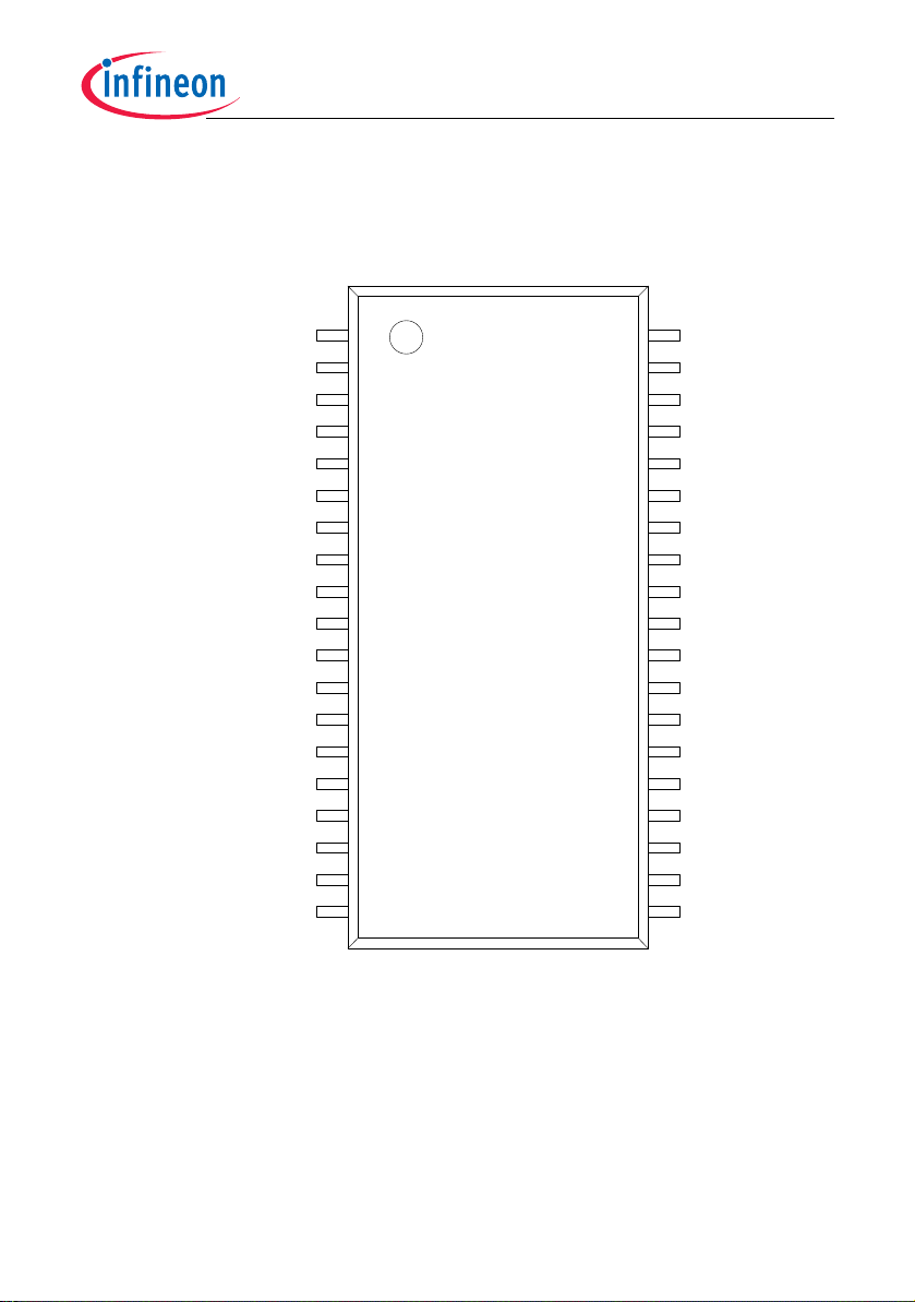
Figure 1 Pin-out of PMA7110 in TSSOP38 package
Preliminary Data Sheet 11 V0.9, 2008-04-28

PMA7110
Functional Description
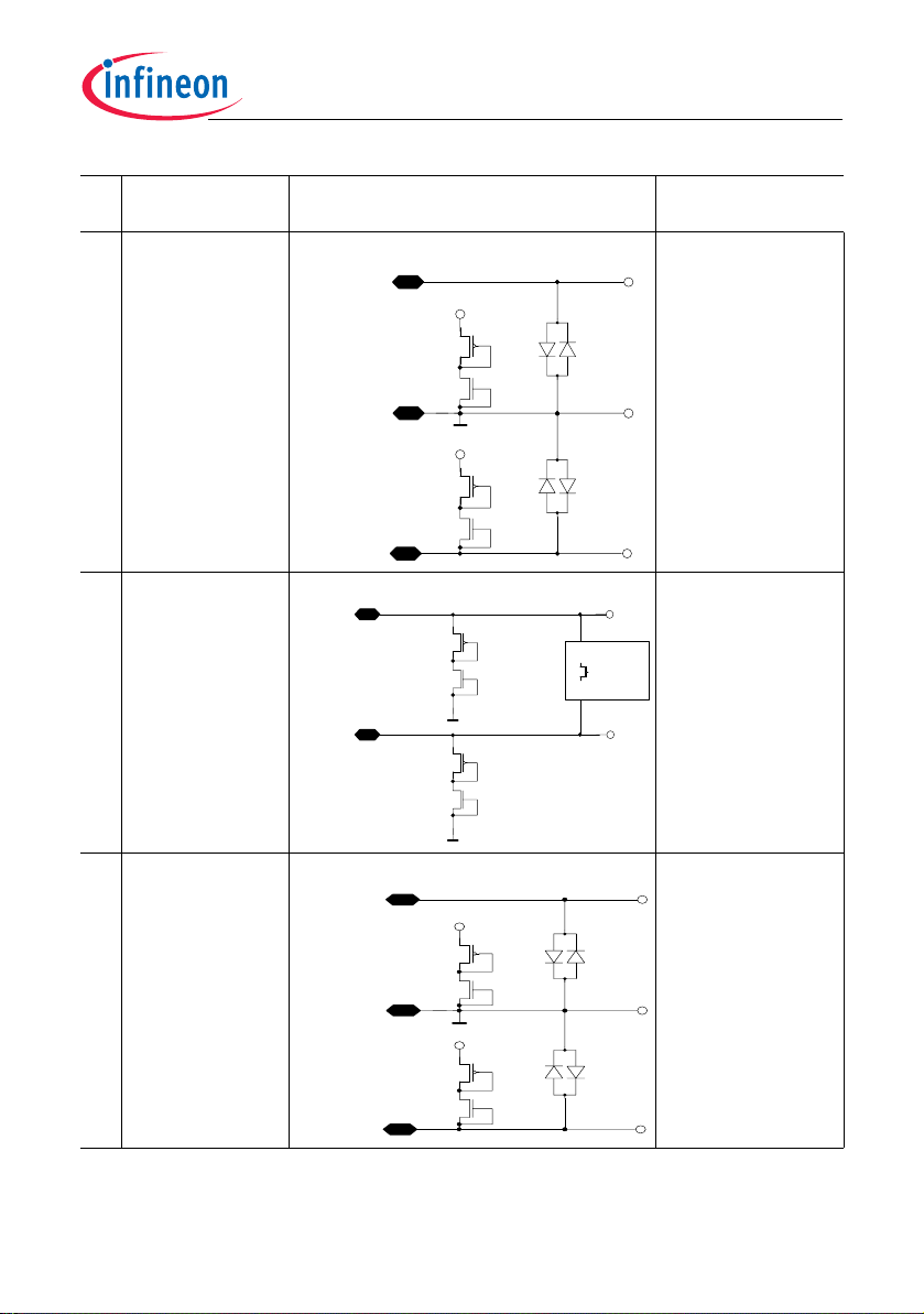
Table 1 Pin Description
Pin Name Type Description Comments
1 VDD(sens.) Supply Sensor positive supply same voltage as chip
2 V1N(sens.) Analog Channel1, negative sensor input output of wheatstone
3 VM1(sens.) Supply Sensor negative supply same voltage as chip
4 V1P(sens.) Analog Channel1, positive sensor input output of wheatstone
5 GNDB Supply Ground
6 GNDA Supply Ground
7 VBat Supply Battery supply voltage
8 PGND Supply RF transmitter ground
9 PA Analog RF transmitter output
10 GND Analog Ground
11 PP2/WU1/
TXDATAOut
12 PP1/WU0/
I2C_SDA/
OPMode2
13 PP0/
I2C_SCL/
OPMode1
14 PP3/SPI_CS/
WU2
15 PP4/WU3
/SPI_MISO
16 PP5/
SPI_MOSI
17 PP6/WU4
/SPI_Clk
Digital GPIO, External wakeup source,
Serial output of
Manchester/Biphase encoded data
Digital GPIO, External wakeup source, I2C
bus interface data, Select operation
mode
Digital GPIO, I2C bus interface clock,
Select operation mode
Digital GPIO, SPI bus interface chip select,
External wakeup source
Digital GPIO, SPI bus interface master in
slave out, External wakeup source
Digital GPIO, SPI bus interface master out
slave in
Digital GPIO, SPI bus interface clock,
External wakeup source
analog supply
bridge sensor
GND
bridge sensor
internal
pullup/pulldown
switchable
internal
pullup/pulldown
switchable
internal
pullup/pulldown
switchable
internal
pullup/pulldown
switchable
internal
pullup/pulldown
switchable
internal
pullup/pulldown
switchable
internal
pullup/pulldown
switchable
Preliminary Data Sheet 12 V0.9, 2008-04-28

PMA7110
Functional Description
Table 1 Pin Description
Pin Name Type Description Comments
18 xReset Digital External reset low active
19 PP7/WU5
/Ext_Int1
20 PP8/WU6 Digital GPIO, External wakeup source internal
21 PP9/WU7
/Ext_Int1
22 MSE Digital Mode select enable high active, set to
23 TME Digital Test mode enable high active, set to
24 XTALCAP Analog Crystal oscillator load capacitance
25 XTAL/SCLK Analog Crystal oscillator input, External
26 XGND Supply Crystal oscillator ground
27 AMUX1 Analog additional differential ADC standard
28 AMUX2 Analog additional differential ADC standard
29 XLF Analog Differential LF receiver Input2
30 LF Analog Differential LF receiver Input1
31 VReg Supply Internal voltage regulator output connect to
32 VDDD Supply Digital supply
33 VDDA Supply Analog supply
34 GNDC Supply Ground
35 RD(sens.) Analog use only by having
Digital GPIO, External wakeup source internal
Digital GPIO, External wakeup source,
External Interrupt source
reference clock
input1 for external sensor
input2 for external sensor
pullup/pulldown
switchable
pullup/pulldown
switchable
internal
pullup/pulldown
switchable
GND in normal mode
GND in normal mode
connect to GND if not
connect to GND if not
decoupling capacitor
diagnostic resistor on
use
use
=100nF)
(C
BCAP
sensor bridge,
otherwise none
connection
Preliminary Data Sheet 13 V0.9, 2008-04-28

PMA7110
Functional Description
Table 1 Pin Description
Pin Name Type Description Comments
36 V2P(sens.) Analog Channel2, positive sensor input output of wheatstone
37 VM2(sens.) Supply Sensor negative supply same voltage as chip
38 V2N(sens.) Analog Channel2, negative sensor input output of wheatstone
bridge sensor
GND
bridge sensor
Preliminary Data Sheet 14 V0.9, 2008-04-28
PMA7110
Functional Description
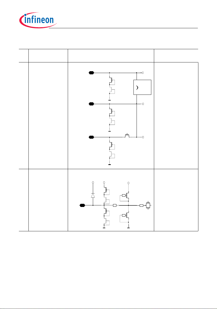
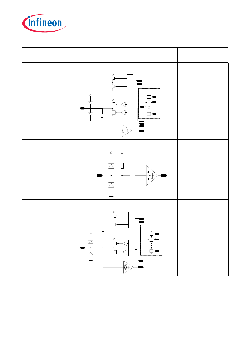
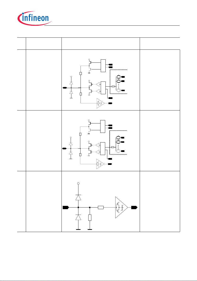
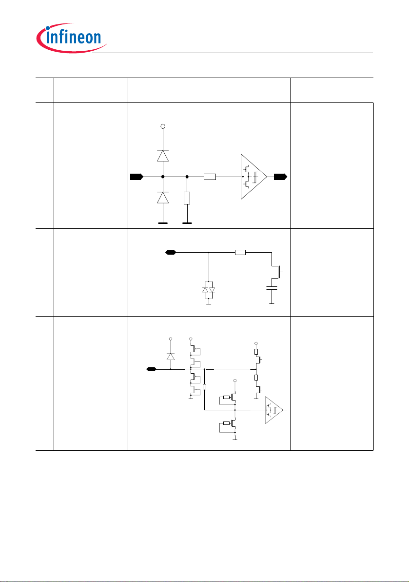
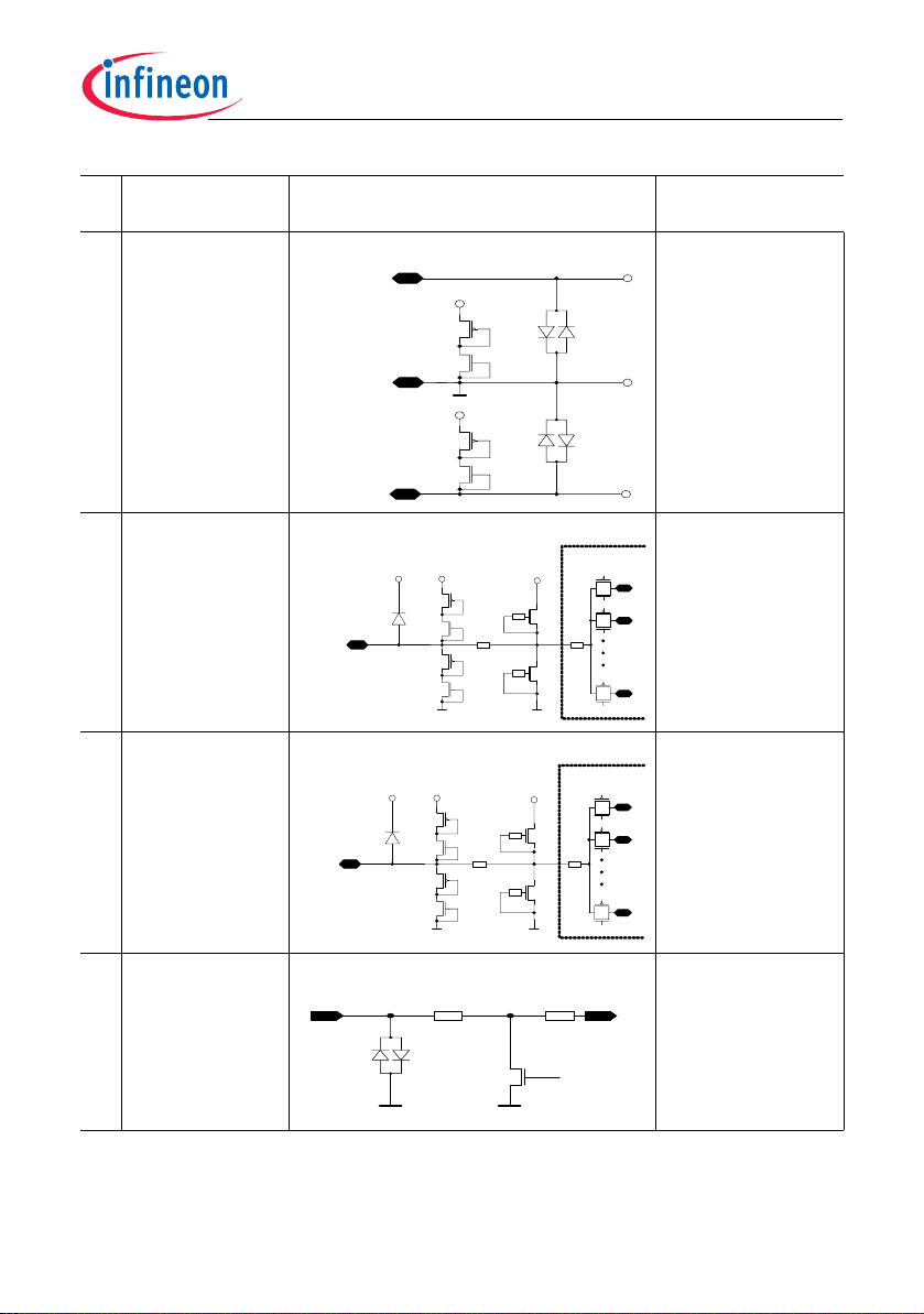
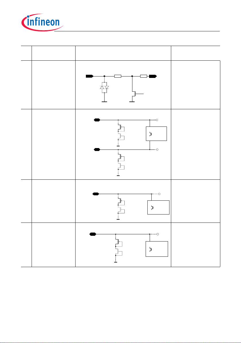
Table 2 Pin I/O equivalent schematics
Pin
PAD name Equivalent I/O Schematic Function
No.
1 VDD (Sens.) Sensor Positive
Volt ag e
Regulator
Supply
VBat
VReg
VDD (sens)
GND
GND
Swit ch
GND
2 V1N (Sens.) Channel 1
Negative Signal
2k
V1N
VDD A
500
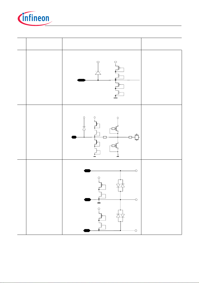
Preliminary Data Sheet 15 V0.9, 2008-04-28
Functional Description
Pin
PAD name Equivalent I/O Schematic Function
No.
3 VM1 (Sens.) Channel 1
VDD A
VM1
GND
Negative Supply
4 V1P (Sens.) Channel 1
VDD A
Positive Signal
PMA7110
V1P
500
2k
5 GNDB Ground
PGND
GNDB
XGND
Preliminary Data Sheet 16 V0.9, 2008-04-28
PMA7110
Functional Description
Pin
PAD name Equivalent I/O Schematic Function
No.
6 GNDA
PGND
GNDA
XGND
7 VBat Power supply
VBat
voltage regulators
Volta ge
Regulator
VReg
8PGND
double bond
PGND
GND
XGND
Power amplifier
ground
Preliminary Data Sheet 17 V0.9, 2008-04-28
PMA7110
t
Functional Description
Pin
PAD name Equivalent I/O Schematic Function
No.
9 PA Power amplifier
10 GND
PA
PROGRAM7V
10
PGND PGND
100
output stage
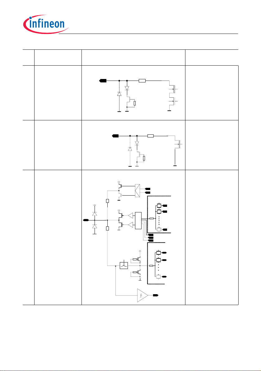
11 PP2/WU1
/TXDATAOut
PP2
VBat
VBat
Pullup
Pulldow n
Tristate
GND
250k
1.8 ... 3.6V
VBat
Data
Tristate
500
GND
AMUX3 TG
Combinatorial
VBat
GND
PPS2
PPO2
Core
DMUX1
2k
Logic
PPD2
TXDATA
RfTXPEn
Core
AMUX3
2k
analog
signals
PPI2
GPIO port
WU1
Serial output of
Manchester/Biphase
encoded data
PPO2
DMUX2
tmd1_xclkdiv
tmd1_wucde
tmd1_lfraw
tmd1_clk_cpu
tmd1_pll_fc
PPO2
0
1
7
Preliminary Data Sheet 18 V0.9, 2008-04-28
Functional Description
Pin
PAD name Equivalent I/O Schematic Function
No.
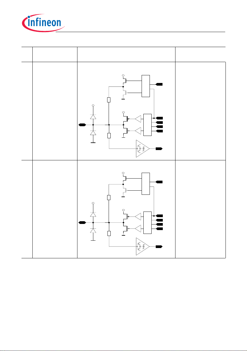
12 PP1/
WU0/I2C_SDA
/OPMode2
VBat
VBat
Pullup
Pulldown
Trist ate
Combinatorial
GND
50k
PPS1
Logic
PMA7110
GPIO port
WU0
I2C_SDA
OPMode2
13 PP0/I2C_SCL
/OPMode1
PP1
PP0
VBat
Data
Data
50k
500
500
VBat
VBat
VBat
GND
GND
Data
Trist ate
Pullup
Pulldow n
Tri stat e
GND
Data
Tristate
PPO1
PPD1
I2CD
Logic
Combinatorial
I2CEn
PPI1
GPIO port
I2C_SCL
OPMode1
PPS0
Logic
Combinatorial
PPO0
PPD0
I2CClk
Logic
Combinatorial
I2CEn
PPI0
Preliminary Data Sheet 19 V0.9, 2008-04-28
Functional Description
Pin
PAD name Equivalent I/O Schematic Function
No.
14 PP3/SPI_CS
/WU2
PP3
VBat
Pullup
Pulldown
Trista te
GND
250k
VBat
Data
Data
Trista te
500
GND
PPS3
Logic
PPO3
Comb i n at or i al
Core
DMUX2
PPO3
DMUX4
DMUX3
2k
tmd2_wucdet
Logi c
Combinatorial
tmd2_lfraw
tmd2_bitbounddet
tmd2_decerr
PPO3
PPD3
PPI3
PMA7110
GPIO port
WU2
SPI_CS
15 PP4/WU3
/SPI_MISO
VBat
PP4
Data
16 PP5/SPI_MOSI GPIO port
VBat
PP5
Data
VBat
Pullup
Pulldown
Trist ate
GND
50k
VBat
Trist ate
500
GND
VBat
Pullup
Pulldown
Tristat e
GND
50k
VBat
Tristate
500
GND
Data
Data
Logic
Combinat ori al
Logic
Combinator i al
Logic
Combinat ori al
Logic
Combinator i al
PPS4
PPO4
PPD4
SPI_MISO
SPIEn
PPI4
PPS5
PPO5
PPD5
SPI_MOSI
SPIEn
PPI5
GPIO port
WU3
SPI_MISO
SPI_MOSI
Preliminary Data Sheet 20 V0.9, 2008-04-28
Functional Description
t
Pin
PAD name Equivalent I/O Schematic Function
No.
17 PP6/WU4
/SPI_Clk
PP6
VBat
Pullup
Pulldown
Tristate
GND
50k
VBat
Data
Data
Tristate
500
GND
PPS6
Logic
PPO6
Combinatorial
Core
DMUX3
PPO6
DMUX5
2k
PPD6
SPI_Clk
SPIEn
PPI6
tmd3_syncmat ch
PPO6
Logic
Combinatorial
GPIO port
WU4
SPI_Clk
18 xReset Reset input
VBat
50k
xRese t
500
Rese
PMA7110
19 PP7/WU5
/Ext_Int1
PP7
VBat
Pullup
Pulldown
Tristate
GND
50k
VBat
Data
Data
Tristate
500
GND
PPS7
Logic
PPO7
Comb i na to r i a l
Core
DMUX4
2k
Logi c
Combinator ial
PPD7
PPI7
GPIO port
WU5
Ext_Int1
PPO7
DMUX6
tmd4_chipvalid
PPO7
Preliminary Data Sheet 21 V0.9, 2008-04-28
Functional Description
Pin
PAD name Equivalent I/O Schematic Function
No.
20 PP8/WU6 GPIO port
PP8
VBat
Pullup
Pulldown
Tristate
GND
250k
VBat
Data
Data
Tristate
500
GND
PPS8
Logic
PPO8
Comb i na t or i a l
Core
DMUX5
HiRC Clock
tmd6_tr_so
2k
Logi c
Combinatorial
tmd5_flash_dig0
PPO8
PPD8
PPI8
WU6
PMA7110
21 PP9/WU7
/Ext_Int0
PP9
Data
250k
VBat
Pullup
Pulldown
Tristate
GND
VBat
Data
Tristate
500
GND
PPS9
Logic
PPO9
Combinatori al
Core
DMUX6
LoRC Clock
tmd5_chip
2k
Logi c
Combinato ri a l
tmd6_flash_dig1
PPO9
PPD9
PPI9
GPIO port
WU7
Ext_Int0
22 MSE Mode Select Enable
VBat
MSE
500
250k
MSE_i
Preliminary Data Sheet 22 V0.9, 2008-04-28
PMA7110
Functional Description
Pin
PAD name Equivalent I/O Schematic Function
No.
23 TME Test Mode Enable
VBat
TME
500
TME_i
250k
24 XTALCAP Crystal oscillator
XTALCAP
10
XGN D XGND
output
25 XTAL/SCLK Crystal oscillator
VDDD
input
SCLK
XTAL
500
XGND
XGND
≈ 0.9Vdc
Bypass
Preliminary Data Sheet 23 V0.9, 2008-04-28
PMA7110
Functional Description
Pin
PAD name Equivalent I/O Schematic Function
No.
26 XGND Crystal oscillator
PGND
GND
XGND
27 AMUX1
Core
2k
GND
AMUX1
VDDA
500
GND
28 AMUX2 Additional
Core
2k
AMUX2
VDDA
500
ground
Additional
differential ADC
standard input1 for
0
external sensor
Analog Testsignal
1
Port
7
differential ADC
standard input2 for
0
external sensor,
1
Analog Testsignal
Port
,
7
GND
GND
29 xLF Low Frequency
xLF
GND
50
xLF_i
15k
Preliminary Data Sheet 24 V0.9, 2008-04-28
Input
PMA7110
Functional Description
Pin
PAD name Equivalent I/O Schematic Function
No.
30 LF Low Frequency
Voltage
Regulator
Input
supply
LF
GND
50
15k
LF_i
31 VReg Regulated Power
VBat
VReg
GND
GND
32 VDDD Digital Supply
1.6 ...2.5 V
VDDD
Digi tal
core
GND
33 VDDA Analog Supply
VDDA
Ana log
core
GND
Preliminary Data Sheet 25 V0.9, 2008-04-28
Functional Description
Pin
PAD name Equivalent I/O Schematic Function
No.
34 GNDC Ground
PGND
GNDC
XGND
35 RD (sens.) Connect to
VDDA
diagnostic resister
on sensor bridge,
otherwise no
connection
RD
500
2k
100k
PMA7110
36 V2P (sens.) Channel 2
VDDA
V2P
500
Preliminary Data Sheet 26 V0.9, 2008-04-28
Positve Signal
2k
Functional Description
Pin
PAD name Equivalent I/O Schematic Function
No.
37 VM2 (sens.) Channel 2
VD DA
VM2
Negative Supply
38 V2N (sens.) Channel 2
VDDA
Negative Signal
PMA7110
V2N
500
2k
Preliminary Data Sheet 27 V0.9, 2008-04-28
2.2 Functional Block Diagram
PMA7110
Functional Description
256 B
RAM
Diff . hig h sens itiv e inp ut1
12MHz RC
HF Os cillat or
V1P
V1N
Diff. high sensitiv e input2
V2P
V2N
Diff. standard input
AMUX1
AMUX2
Vmin
and
TMAX
detec tor
Voltage R egulat ors
Low
power
V-reg
Vbat
Vreg
Input multiplexer
B
ADC
T
Low
dropout
V-reg
VDDA
VD DD
Reference
volt age &
offset DAC
ADC state
machine
Bandgap and
PTAT
PRNG
GN D
ADC
Brownout
detect or
Interval timer
Figure 2 PMA7110 Block Diagram
6 kB
6 kB
Flash
Flash
Mic rocontroller
wit h 8051 core
Interrupt controller
Sys tem c ontrolle r
Reset
Cloc k cont roller
Timer calibration
2kHz RC
LP
Osci llator
12 kB
ROM
Wake U p
Test Controller
Power Mgm
Specia l
function
registers (SFR)
General Purpos e
Input/Output
(GPIO, I2C, SPI,
WU…)
RF transmitter
RF-PLL
Codes
modulat or
Manchester 101 Phase
LF rec eiver
Digi tal
Receiver
detec tor
CRC
generator
ASK
Carrier
Watch
dog
timer
...
Power
Amp
Crystal
Oscillator
FSK
modulat or
125kH z
Receiver
Timer
PP0
PP1
PP2
PP9
...
xReset
PA
PGND
XTAL
XTALCAP
XGND
LF
xLF
MSE TME
Preliminary Data Sheet 28 V0.9, 2008-04-28
Functional Description
2.3 Operating Modes and States
The PMA7110 can be operated in four different operating modes.
•NORMALmode
•PROGRAMMINGmode
• DEBUG mode
• (internal production TEST mode)
2.3.1 Operating mode selection
SYSTEM RESET **
POR, xReset
Software reset
Brown-o ut event
PMA7110
TME = 1
SCAN Test
Mode
MSE = 1
PP0=0
PP1=1
Lockbyte II not set
PROGRA MMING
Mode
MSE = 1
PP0=0
PP1=0
TEST M ode 0 * DEBUG Mode
SFR CFG0.3=0
Functional
Test mode
TME = 0
Mode
Select
MSE = 1
PP0=1
PP1=0
Lockbyte II
not se t
NORMAL
L
o
S
c
F
k
R
b
y
C
t
e
F
G
I
I
0
n
.
3
o
*Note: If Lockbyte I and/or II is set, only a reduced
=
t
1
s
Test command set is ava ilable
e
t
**Note: Whenever TME is set to high the current
operation mode is left and SCAN Test mode is
entered, regardle ss if there was a reset event or not!
MSE = 0
or
MSE = 1
PP0=1|1|0
PP1=1|0|1
Lockbyte II set
or
MSE = 1
PP0=1
PP1=1
Lockbyte II
not set
Mode
Figure 3 Operating mode selection of the PMA7110 after Reset
The Mode Select is entered after the System Reset expires and SCAN Test mode is not
selected. The levels on the the I/O pins PP0 and PP1 are latched by the System
controller and read by the operating system to determine the mode of operation of the
device according to Table 3 "Operating mode selection after Reset" on Page 30.
Therefore also the status of MSE and Lockbyte II from the FLASH are checked. The
Preliminary Data Sheet 29 V0.9, 2008-04-28

PMA7110
Functional Description
MSE, PP0 and PP1 levels must not change after reset release during the whole t
MODE
period (see Figure 5 "Power On Reset - operating mode selection" on Page 32).
Table 3 Operating mode selection after Reset
TME MSE Lock
3.)
x x x x SCAN external Test
1
PP0 PP1 Operating
byte II
mode
Devicecontrol Hardware
restrictions
n.a.
machine
0 0 x x x NORMAL CPU executing
Flash write disabled
from 4000h
0 1 x 0 0 TEST TEST mode
None
handler
01not
0 1 set 0 1 NORMAL CPU executing
0 1 PROGRAMMING PROGRAM
set
None
mode handler
Flash write disabled
from 4000h
01not
0 1 set 1 0 NORMAL CPU executing
1 0 DEBUG DEBUG mode
set
Flash write disabled
handler
Flash write disabled
from 4000h
0 1 x 1 1 NORMAL CPU executing
Flash write disabled
from 4000h
1.) Flash protection is done by hardware. In these modes setting the SFR bits FCS.3 [PROG] and FCS.2 [ERASE]
is not possible.
2.) Flash programming and erasing is only possible via ROM Library functions.
3.) Whenever TME is set to high the current mode is left immediately and SCAN Test Mode is entered, regardless
if there is a reset or not.
2)
2.)
2.)
2.)
2.)
Preliminary Data Sheet 30 V0.9, 2008-04-28

PMA7110
e
Functional Description
.
MSE = 0
Mode
Select
or
MSE = 1
PP0=1|1|0
PP1=1|0|1
Lockb yte II set
or
MSE = 1
PP0=1
PP1=1
Lockb yte II
not set
WD
INIT
WD
WU
IFLG
IDLE
IDLE
RUN
RS
IRQRETI
PE
PDWN
Figure 4 NORMAL Mode - State transistion diagram
For low power consumption and safety reasons the PMA7110 supports different
operating states - RUN state, IDLE state and POWER DOWN mode and Thermal
shutdown state. The device operation in these states is described below.
Transitions between these states are either application software controlled or managed
automatically by the system controller.
- PDWN: Powerdown (CPU & Peripherrals stopped)
- IDLE: CPU clock stopped, peripherals are still running
States
TSHT - Thermal shutdown
PDWN - Powerdown
RUN - Run application
IDLE - CPU clock stopped
TE
TSHT
WU
Transitions
WU - Wakeup
PE - Powerdown enable
TE - Thermal shutdown enabl
WD - Watchdog
IFLG - Idle flag
RS - Resume
IRQ - Interrupt request
RETI- Return from interrupt
Preliminary Data Sheet 31 V0.9, 2008-04-28

Vreg
RESET
(internal)
PP0, PP1
V
V
PMA7110
Functional Description
THR
POR
t
POR
t
MODE
Figure 5 Power On Reset - operating mode selection
During the time t
, the levels of PP0, PP1 and MSE are read, and being determined
MODE
the operation mode of the device according to Table 3 "Operating mode selection
after Reset" on Page 30. The levels on these pins must be stable during the whole
period.
t
MODE
The PMA7110's Power On Reset circuit is activated if Vreg rises above V
internal blocks are held in Reset state until Vreg has risen above V
When this Reset state is released, a further time of t
on PP0, PP1 and MSE. After t
has elapsed, the device starts operation in the
MODE
is needed for reading the levels
MODE
THR
.
POR
. The
selected mode.
Note: See “Power On Reset” on Page 138 for details on Power On Reset
characteristics.
2.3.2 State Description
2.3.2.1 INIT State
This is a transient state which is entered when the settings of PP0, PP1, MSE, TSE and
the Lockbyte II lead to Normal Mode (please refer to Table 3 "Operating mode
selection after Reset" on Page 30). In this state, the SFRs which are not located in the
System controller get reset and the ROM routines initializes the system to its default
Preliminary Data Sheet 32 V0.9, 2008-04-28

PMA7110
Functional Description
values. Then the application Program in Flash is started at 4000h and the device enters
RUN state.
2.3.2.2 RUN State
In RUN state the CPU8051 executes programs stored in ROM or FLASH memory.
Peripherals are on or off according to the application program. The watchdog (WD) is
active and automatically cleared when entering RUN state on a Wakeup event. The CPU
clock frequency is selectable by software. All Wakeup events are ignored in RUN state
but the corresponding flags get set and can be read and cleared.
2.3.2.3 IDLE State
In IDLE state, the CPU8051 clock is disabled but Peripherals (Timers, ADC, RF-TX, SPI,
2
C Interface and Manchester/Biphase Coder) continues normal operation. If a resume
I
condition occurs the RUN state is reentered immediatelly. The watchdog (WD) is active
and reset automatically when entering IDLE state. All wakeups are ignored in IDLE state
but the corresponding flags are set if a wakeup occurs and can be evaluated once the
device returns to the RUN state.
In case of a Peripheral requests, an interrupt or an External Interrupt occurs the IDLE
state is left for RUN state, the Interrupt service routine is executed and on the next RETI
(return from interrupt) instruction the IDLE State is re-entered in case no Resume event
has occured in between.
Resume events:
The resume source can be identified by reading REF. Resume events may occur on
following events:
• RF transmitter buffer empty.
• RF transmission finished.
• LF receiver buffer full.
• Timer 2 underflow.
• A/D conversion finished.
• RC-LP-Oscillator calibration finished.
• Clock change from RC-HF-Oscillator to Crystal-Oscillator finished.
Interrupt requests:
Interrupts during IDLE state may be requested by embedded peripherals or external
events.
• External (Pin) Interrupt 0/1
• Timer 0/1/2/3
Preliminary Data Sheet 33 V0.9, 2008-04-28

PMA7110
Functional Description
• I2C Interface
• SPI Interface
•LF Receiver
•RF Encoder
2.3.2.4 POWER DOWN State
In POWER DOWN state the CPU8051 and its peripherals are powered down. The
system controller, its SFRs, the XData memory and optional the lower 128 byte internal
RAM are kept powered. The LF receiver will be switched on periodically if the LF on/off
timer is enabled. Wakeup flags are cleared automatically when going to POWER DOWN
or THERMAL SHUTDOWN.
Wakeup Events:
A wakeup event occurs when a peripheral or external source causes the system to
power up again. The wakeup source can be identified by reading SFRs WUF and
ExtWUF. Wakeup Events may occur on following events:
• At least one of the External Wakeup Pins changed its state to the configured one
• Interval Timer underflow occured
• LF receiver carrier detected
• LF receiver pattern matched
• LF receiver sync matched
• Watchdog timer elapsed
2.3.2.5 THERMAL SHUTDOWN state
In THERMAL SHUTDOWN state, only the TMAX circuit can provide a wakeup event. All
other wakeup sources are disabled. The device will remain in this state until the
temperature falls below the T
Page 41 for details).
Preliminary Data Sheet 34 V0.9, 2008-04-28
threshold (see “Functional Block Description” on
REL

PMA7110
Functional Description
2.3.2.6 State Transitions
With reference to Figure 4 "NORMAL Mode - State transistion diagram" on Page 31,
the following state transitions can occur:
Table 4 State Transitions in NORMAL mode
State transition Description
RUN state
=> IDLE state (IFLG)
IDLE state
=> RUN state (RS, IRQ)
IDLE state
=> INIT state (WD)
RUN state
=> INIT state (WD)
RUN state
=> THERMAL SHUDOWN state
(TE)
RUN state
=> POWER DOWN state
(PDWN)
The application program can set SFR bit CFG0.5[IDLE]1) to
enter IDLE state. Note that the next opcode should be a NOP
instruction.
(see Table 11 "SFR Address F8
Register 0" on Page 58)
Note: If no peripheral that can create a RESUME event is
active, IDLE state will not be entered and the application will
continue operation.
RS: A peripheral unit (Timer 2, ADC, RF transmitter,
LF receiver, System Clock source switch) creates a resume
event. The application continues with the instruction after the
Idle bit setting (see Table 20 "SFR Address D1
Resume Event Flag Register" on Page 67).
IRQ: An interrupt occurs. This interrupt allows the immediate
execution of the interrupt service routine. With the return from
interrupt instruction the device returns to IDLE state if no
resume event has been generated in between.
Overflow of the watchdog timer. The application will restart by
initialization of the SFRs that are located outside the SFR
Container. No Mode selection is possible, the Normal Mode is
not left. The watchdog wakeup may be identified by Table 18
"SFR Address C0H: WUF - Wakeup Flag Register" on
Page 65
The application should enter Thermal Shutdown state
whenever it detects that the specified operating temperature
maximum of 125°C has been overreached to avoid
malfunction of the device. This is done by setting the
CFG0.6 [TSHDWN]. Alternatively this can be done via ROM
library function.
Note: If the temperature is below the TMAX threshold the
device immediately generates a WU event and re-initializes
the system
Entering this state is always software controlled by setting
CFG0.7[PDWN]. The application program can call a
ROM Library function to enter POWER DOWN state
whenever needed.
: CFG0 - Configuration
H
: REF -
H
Preliminary Data Sheet 35 V0.9, 2008-04-28

PMA7110
Functional Description
State transition Description
THERMAL SHUTDOWN state
=> RUN state (WU)
POWERDOWNstate
=> RUN state (WU)
INIT state
=> RUN state
1)1) Note: It is mandatory that the instruction setting the CFG0.5[IDLE] is followed by a NOP instruction.
The TMAX circuit generates a wakeup event when the
temperature falls below TMAX threshold.
A wakeup event will restart the application and set the SFR
WUF resp. ExtWUF accordingly. The Watchdog timer is reinitialized (see Table 19 "SFR Address F1H: ExtWUF -
Wakeup Flag Register 2" on Page 65). Wakeup duration
from POWER DOWN mode to RUN state typically lasts 1410
µs. The time is the sum for the power supply to get stable
(100µs), the startup time of the oscillator (1150 µs) and the
time for the operating system to get initialized
(160µs @12MHz CPU8051 clock).
This state change is initiated automatically by the system
controller as soon as INIT state is finished.
Preliminary Data Sheet 36 V0.9, 2008-04-28

PMA7110
Functional Description
2.3.2.7 Status of PMA7110 Blocks in Different States
Depending of the actual state in NORMAL mode the internal blocks of the PMA7110 are
active, inactive or have no supply to reduce power consumption. The next table gives an
overview over the different blocks in the different device states.
Table 5 Status of important PMA7110 blocks in different states
Peripheral unit RUN state IDLE state POWER DOWN
state
Power on reset active active active active
Brown-out detector active active inactive
power down
Power supply - Low
drop voltage regulator
Low power voltage
supply
System controller active active active active
Wakeup Logic active active active active
CPU8051 active inactive no supply no supply
Non-volatile SFRs
(System Controller)
Peripheral core
SFR’s
Manchester/Biphase
Coder, Timer
Pheripheral modules CRC, MFLSR
Peripheral modules
-I2C, SPI, ADC
Watchdog active active no supply no supply
active active inactive
power down
(Remark:
can be enabled
by LF-RX)
active active active active
active inactive
content not
lost
active inactive
content not
lost
software
selectable
software
selectable
software
selectable
software
selectable
inactive no supply no supply
software
selectable
inactive
content not lost
no supply content lost
no supply no supply
no supply no supply
THERMAL
SHUTDOWN state
inactive
power down
inactive
power down
inactive
content not lost
no supply - content
lost
Preliminary Data Sheet 37 V0.9, 2008-04-28

PMA7110
Functional Description
Peripheral unit RUN state IDLE state POWER DOWN
state
RAM Lower 128Bytes active inactive
content not
lost
selectable
power down
(content lost) or
inactive
THERMAL
SHUTDOWN state
selectable power
down (content lost)
or inactive (content
not lost)
(content not lost)
RAM Upper 128Bytes active inactive
content not
no supply content lost
no supply - content
lost
lost
XData 16 bytes active inactive
content not
inactive
content not lost
inactive content not
lost
lost
FLASH memory active inactive
content not
no supply
content not lost
no supply
content not lost
lost
ROM active inactive no supply
content not lost
Crystal oscillator software
selectable
software
selectable
inactive
power down
no supply
content not lost
inactive
power down
2kHz RC-Oscillator active active active inactive
power down
12MHz
RC-HF-Oscillator
software
selectable
software
selectable
power down
(Remark:
power down
can be enabled
by LF-RX)
Interval timer active active active inactive
LF Receiver software
selectable
RF Transmitter software
selectable
software
selectable
software
selectable
software
selectable
inactive
power down
inactive
power down
inactive
power down
Preliminary Data Sheet 38 V0.9, 2008-04-28

PMA7110
Functional Description
Peripheral unit RUN state IDLE state POWER DOWN
state
Vmin Detector software
selectable
software
selectable
no supply inactive
THERMAL
SHUTDOWN state
power down
Note: active: block is powered, is active and keeps its register contents. Power
consumption is high
inactive: block is powered, cannot be used, but keeps its register contents.
Power consumtion is low
no supply: block is not powered, connot be used and all register content is lost.
Power consumption is zero
Preliminary Data Sheet 39 V0.9, 2008-04-28

PMA7110
Functional Description
2.4 Fault protection
The PMA7110 features multiple fault protections which prevent the application from
unexpected behavior and deadlocks. This chapter gives a brief overview of the available
fault protections. Detailed explanation of the usage can be found later in this document
and in [1] “Reference SFR Registers” on Page 144.
2.4.1 Watchdog Timer
For operation security a watchdog timer is available to avoid application deadlocks. The
watchdog timer must be reset periodically by the microcontroller, otherwise the timer
generates a software reset and forces a restart of PMA7110 program execution.
The watchdog timer duration is fixed to nominal 1 second. The accuracy depends on the
accuracy of the 2 kHz RC LP Oscillator which is used to clock the watchdog timer.
Setting SFR bit CFG2.1[WDRES] resets the watchdog timer (see Table 13 "SFR
Address D8
: CFG2 - Configuration Register 2" on Page 60).
H
2.4.2 VMIN Detector
This circuit will detect if the supply voltage is below the minimum value required to
guarantee the measurement accuracy. The ROM library functions which perform
measurements will return the VMIN status in a statusbyte with the measurement result.
2.4.3 FLASH Memory Checksum
A CRC checksum is stored in the FLASH memory, and can be recalculated and checked
by the application program for verification of program code if needed.
Flash bit FCSP.7[ECCErr]: If a single bit error in the Flash memory occurs it is corrected
by the Flash internal Error Correction Coder, as an indication the FCSP.7[ECCErr] bit is
set. (see Table 101 "SFR Address E9
: FCSP- Flash Control Register - Sector
H
Protection Control" on Page 146 in “Reference SFR Registers” on Page 144)
2.4.4 ADC Measurement Overflow & Underflow
The ROM Library functions which perform measurements will return the over/underflow
status in a statusbyte with the measurement result.
2.4.5 TMAX Detector
The TMAX detector is used to wakeup the PMA7110 from
THERMAL SHUTDOWN state if the ambient temperature falls below the trigger level
T
.
REL
Entering THERMAL SHUTDOWN state can be initiated by a ROM Library function
described in [1] “Reference Documents” on Page 157.
Preliminary Data Sheet 40 V0.9, 2008-04-28

PMA7110
Functional Description
2.5 Functional Block Description
2.5.1 Sensor Interfaces and Data Acquisition
The PMA7110 has two internal sensors, two high sensitive differential analog interfaces
4 programmable gainfactors (from 76+-20%, 60+-20%, 50+-20% and 38+-20% ) and
one standard differential analog interface (gainfactor 1) to acquire environmental data:
• Temperature Sensor
• Battery Voltage Monitoring
• external data through analog interface
The analog data is aquired and digitalized by the internal 10 Bit ADC. Measurement
routines for acquiring data are available within the ROM library functions that are
described in [1] “Reference Documents” on Page 157.
2.5.1.1 Sensor Interface
SFR CFG2.3 PDADC
SFR CFG1 .3
SFR REF.5
SFR ADCM
SFR ADCS
SFR ADCC1
SFR ADCC0 STC[2:0]
SFR ADCC1
SFR ADCOFF
SFR ADCDH
SFR ADCDL
SFR ADCM
ADCEn
READC
SARSATL
SARSATH
CL000
CG3FF
SAMPLE
BUSY
GAIN[1:0]
FCnSC
SUBC[2: 0]
TVC[2:0]
GAIN[1:0]
OFF[5:0]
Data[9:8]
Data[7:0]
RV[2:0]
CS[2:0]
EOC
Sensor Interface
MUX
Channel 0
CSI
Logi c
Control
Channel 1
Channel 2
Channel 3
Channel 4
A
D
C
Channel 5
Channel 6
Ch5p,Ch5n
Ch6p,Ch6n
Ch0p,Ch0 n
Ch1p,Ch1n
Ch2p,Ch2n
Ch3p,Ch3n
Ch4p,Ch4n
Battery Sensor
Temper ature
Sensor
Sta ndard
Sens or Int erfac e
Bandga p
Reference
VRe g Sensor
External
Sensor
Interface
AMUX1
AMUX2
VDD (sens.)
VDD (sens.)
V1P (sen s.)
V1N (sens.)
VM1 (sens.)
Channel 7
Ch7p,Ch7n
V2P (sens.)
V2N (sens.)
VM2 (sens.)
RD (sens.)
Figure 6 Block diagram Sensor Interface
The sensor interface connects to the external sensors and to the internal (on-chip)
temperature and battery voltage sensors.
Preliminary Data Sheet 41 V0.9, 2008-04-28

PMA7110
Functional Description
All signal channels can be configured for differential or single-ended operation.
Differential operation is only recommended for signals where the common-mode voltage
is stable, while the positive and negative signal voltages vary symmetrically around the
common-mode voltage.
The input multiplexer selects one channel for the input signal and one channel for the
reference voltage to the ADC. Any channel can be selected as reference, except
channels 6 and 7, which are specially adapted to the low level signals from external
sensors.
Preliminary Data Sheet 42 V0.9, 2008-04-28

PMA7110
Functional Description
2.5.1.2 Two differential high sensitive interfaces to external Sensors
Differential high sensitive sensor interface 1( (Channel 6)
V1P/V1N is the positve/negative differential voltage inputs of the first sensor bridge.
Differential high sensitive sensor interface 2 (Channel 7)
V2P/V2N is the positve/negative differential voltage inputs of the second sensor bridge.
Channel gain selection
The SFR Bit ADCC1.5-4 [GAIN1-0] gain factor selection allows the selection of the
sensitivity of the analog input channels 6 and 7. The gain is one for all other input
channels (see Table 6 ).
Table 6 Selection of the gain factor
Gain factor
(gain)
76 +/- 20% 11X 0 0
60 +/- 20% 11X 0 1
50 +/- 20% 11X 1 0
38 +/- 20% 11X 1 1
1others00
1others01
1others10
1others11
Channel
ADCM.CS2-0
GAIN1 GAIN0
Sensor Excitation
The two sensor bridges have a common positive supply which is always connected.
When a sensor bridge is to be activated, its negative supply is pulled to ground by
pad VM1 or VM2 for VMP or VMA. Otherwise, it is disconnected. In this way the power
of a connected bridge can be supplied.
Preliminary Data Sheet 43 V0.9, 2008-04-28

PMA7110
Functional Description
These two sensor interfaces are very adapted piezoresistive Wheatstone bridge
sensors, whose output signal is differential and ratiometric (proportional to the bridge
excitation voltage). The electrical configuration is shown as a example in figure below..
V1P
VM1
V1N
VDD
V2P
VM2
RD
V2N
Figure 7 Wheatstone bridge sensor
2.5.1.3 Interface to other signals
Battery voltage Interface (Channel 0)
The positive input to the battery voltage signal is derived by dividing voltage V
by 3.5.
Bat
The negative input is connected to GND. The battery voltage is converted with a
resolution of approximately 4.1mV, using channel 3 as reference.
Temperature Sensor Interface (Channel 1)
The temperature signal to the ADC is a single ended signal, with the PTAT voltage
between 500 and 1100 mV. The temperature sensor signal is digitized with a resolution
of approximately 0.5°C, using channel 3 as reference.
Standard sensor Interface (Channel 2)
The positive input signal is available at AMUX1, and the negative input at AMUX2.
2.5.1.4 Reference voltages
When channel 6 or 7 is selected as input to the ADC, and the negative external sensor
supply is identical to the negative supply of ADC, this negative supply should be selected
by the multiplexer as reference voltage on channel 5.
Preliminary Data Sheet 44 V0.9, 2008-04-28

PMA7110
Functional Description
If the negative external sensor supply (which should be used as reference voltage to
external sensor) is not identical to the negative supply of ADC, it should be connected to
the Channel 2 so that it can be selected by multiplexer as reference voltage for channel
6 or 7. But the supply voltage of the external sensor must always be within the range
GND to V
BATT
ch2p
ch2n
PMA7110
External
Supply
+
-
Sensor
ch6p
ch6n
Voltage
Figure 8 External Sensor use channel 2 as reference voltage
Additional 3 channels on ADC input multiplexer carry voltages which are intended as
reference voltages for the converter:
BANDGAP Reference (Channel 3)
This reference is a nominal voltage of 1210 mV. It is intended as reference for the
temperature and V
VREG Reference (Channel 4)
This reference is the V
and is meant as reference for the test signal, to allow as large test signal as possible.
BRIDGE SUPPLY Reference (Channel 5)
When channel 6 or 7 is selected as input to the ADC, the reference voltage is the bridge
supply voltage. A multiplexer selects the appropriate negative bridge supply.
measurements.
Bat
voltage. This is the largest allowable input voltage to the ADC,
REG
Preliminary Data Sheet 45 V0.9, 2008-04-28

PMA7110
Functional Description
2.5.1.5 Temperature Sensor
Temperature measurement is performed by a dedicated ROM library function.
See “Temperature Sensor Characteristics” on Page 128 for the sensor specification.
2.5.1.6 Battery Voltage Monitor
Battery Voltage measurement is performed by a dedicated ROM library function.
See “Battery Sensor Characteristics” on Page 128 for the sensor specification.
Preliminary Data Sheet 46 V0.9, 2008-04-28

PMA7110
Functional Description
2.5.2 Memory Organization and Special Function Registers (SFR)
Nonvolati le
Code
memory
0xFFFF
0x5900
0x58FF
0x58C0
0x58BF
0x5880
0x587F
0x5800
0x57FF
0x5780
0x577F
0x4033
0x4000
0x3FFF
0x3003
0x3002
0x3000
0x2FFF
0x007F
0x0000
FLASH
6kB
ROM
12 kB
Not implemented
Reference c ells
64B
64B
128B
128B
6016B
Lockbyte 1
Flas h Configurat ion + ID
User Data Sector II
Lockbyte 3
User Data Sector I
CRC Sum + Loc kbyt e 2
Code
Vect ors
Not implemented
SFR mapped SRAM
Revision number, Checksum
Mode Handlers
Library Functions
Vect ors
Figure 9 Memory map
The following memory blocks are implemented:
RAM
256
byte
RAM
16
byte
Data
memory
Data
Optional battery buffered
Data RAM
Indirect
addressing
SFR
Direct
addressing
Xdata
memory
Battery buffered Data RAM
acce ssib le w i th
movx
0xFF
0x80
0x7F
0x00
0x0F
0x00
• 12 kByte ROM Memory
• 3 Byte SFR mapped Code Memory
• 6 kByte Flash Code Memory
• 2x128 Bytes FLASH User Data Memory
• 128 Bytes Flash Configuration, ID and Reference cells
• 2 x 128 Byte Data RAM / thereof 128 bytes battery buffered optionally
• 16 bytes battery buffered XData RAM
Preliminary Data Sheet 47 V0.9, 2008-04-28

PMA7110
Functional Description
2.5.2.1 ROM
A 12 kB ROM memory is located in address range 0000H to 2FFF
ROM library functions and Reset/Wakeup Handlers
The ROM contains the reset handler, the wakeup handler and the ROM Library functions
(see [1] “Reference SFR Registers” on Page 144).
A hardware mechanism is implemented to prevent direct jumping into the ROM area,
thus access to the ROM library functions is granted via a vector table at the bottom of
the ROM address space.
ROM protection
To protect the ROM code against readout a hardware mechanism is implemented, thus
a read operation from the ROM in the protected address area returns zero.
.
H
Preliminary Data Sheet 48 V0.9, 2008-04-28

PMA7110
Functional Description
2.5.2.2 FLASH
FLASH Organization
The FLASH is divided into five sectors. Each sector can be erased and written
individually (Bytewise erasing and writing is not possible).
• 4000H -- 577FH (6016 Bytes) code sector (sector 0): This sector contains the Code
sector for the application program.
• 5780
-- 587FH (2x128 Bytes) User Data sector I + User Data sector II (sector 1
H
+ sector 2): These two sectors contain the User Data Sector which can store
individual device configuration data. It also contains the crystal frequency which is
needed for the ROM Library functions.
• 5880H -- 58BFH (64 Bytes) configuration sector (sector 3): This sector contains
the FLASH configuration sector for FLASH driver parameters.
• 58C0
-- 58FFH (64 Bytes) reference cells sector (sector 4): This sector contains
H
the reference current generator cells for FLASH reading.
FLASH protection
Write and erase operations on the Flash Code Sector are only allowed in
PROGRAMMING mode. To protect the FLASH against unauthorized access three
lockbytes can be set:
• Lockbyte 1: Address 0x58FF (Top address of Flash Configuration + Reference Cells
Sector).
This is written in the end of production test. Whenever the Resethandler detects this
value the FCSP.0[ConfLock] gets set and the Reference Cells Sector, Flash
Configuration Sector are irreversibly switched to read-only.
• Lockbyte 2: Address 0x577F (Top address of the Code Sector).
This byte is written (also a ROM CRC) by the Programmer together with the Code
download. When the Resethandler detects this byte it sets the FCSP.1[CodeLCK]. In
addition the Debug Mode, Programming Mode and Test Mode are no longer
accessible. Their pin settings lead to Normal Mode and reduced TM wherein the CRC
can be checked (pass/fail) and the whole Flash can be erased to reset the chip to
shipping state. This Lockbyte has to be set during programming the Code Sector to
protect application code against undesired read-out.
• Lockbyte 3: Address 0x587F (Top address of the User Data Sector I and User Data
Sector II).
There is a ROM Library function for setting this byte. (Therefore the data in the User
Preliminary Data Sheet 49 V0.9, 2008-04-28

PMA7110
Functional Description
Data Sector have to be captured into RAM, the Lockbyte added, the whole sector
erased (Flash!) and re-written. Whenever the Resethandler detects this value
DSR.0[FlashLCK] gets set. When not written together with the Code Sector the User
Data Sector is planned to be written in Normal Mode (from the Customer) using ROM
Library functions. There is a HW mechanism that blocks access to the Flash
Registers when operating from the Flash (not ROM). In this way, the usage of ROM
Library functions is guaranteed, they ensure several important details not to damage
the chip. If Lockbyte 3 is set without setting Lockbyte 2, this byte shows no effect and
will result a unlocked FLASH. How to set Lockbyte 3 is described in “FLASH Set
Lockbyte 3” on Page 121.
Preliminary Data Sheet 50 V0.9, 2008-04-28

PMA7110
e
Functional Description
2.5.2.3 RAM
The RAM is available as data storage for the application program. ROM library functions
may use some RAM locations for passing parameters and internal calculations. The
RAM area which is used for the ROM library functions is specified in [1] “Reference
Documents” on Page 157.
The RAM is always powered in RUN state and IDLE state.
The upper 128 bytes of RAM are always switched off in POWER DOWN state and
THERMAL SHUTDOWN state and lose their contents in these states.
SFR bit CFG2.4[PDLMB] determines if the lower 128 bytes of RAM are powered during
POWER DOWN state and THERMAL SHUTDOWN state.
If not powered in these states, this RAM loses the content, otherwise it can be used as
battery buffered storage beyond a POWER DOWN period.
Note: The RAM is not reset at a System Reset. After a Brown Out Reset this feature can
be used to possibly recover data from RAM.
After Power On Reset the RAM is not initialized, thus it contains random data. The
application has to initialize the RAM if needed.
2.5.2.4 Special Function Registers
Special Function Registers are used to control and monitor the state of the PMA7110
and its peripherals. The following table shows the naming convention for the SFR
descriptions that are used throughout this document.
R/C/W - 0/0
Value after Power On Reset
Value after wakeup from POWER DOWN / THERMAL SHUTDOWN stat
x ... unknown
u ... unchanged
1 ... high
0 ... low
Access:
R ... Readable
C ... Cleared after Read / automatically cleared
W ... Writeable
Figure 10 Naming convention for Register descriptions
Note: If a single bit or the whole byte value is declared as unchanged, it keeps its state
even during POWER DOWN state or THERMAL SHUTDOWN state.
Table 7 "SFR Special Function Register Address Overview" on Page 53 shows all
available registers of the PMA7110.
Note: All SFRs that are listed in Table 7 "SFR Special Function Register Address
Overview" on Page 53 but not in Table 8 "Status of SFR Registers in
Preliminary Data Sheet 51 V0.9, 2008-04-28

PMA7110
Functional Description
POWER DOWN state" on Page 53 should not be changed by the application
since they could be damaged irreversibly. These are handled automatically by the
ROM Library functions if needed.
Preliminary Data Sheet 52 V0.9, 2008-04-28

PMA7110
Functional Description
Table 7 SFR Special Function Register Address Overview
Addr Regis ter A ddr Register Addr Register Addr Register Addr Register Addr Register Addr Register Addr Re gister
F8 CFG0 F 9 LFRXC FA FB FC FD F E FF
F0 B F1 EXTWUF F2 EXTWUM F3 SP IB F4 SPIC F5 SPID F6 SPIM F7 SPIS
E8 CFG1 E9 FCSP EA FCS EB P3DIR EC P3 IN ED P3SENS EE RFC EF LB D
E0 ACC E1 FCPP 0 E2 FCPP1 E3 FCSERM E4 FCTKAS E5 FCSS E6 RFS E7 RFENC
D8 CFG2 D9 DSR DA ADCOFF DB ADCC0 DC ADCC1 DD ADWBC DE RFVCO DF RFFSLD
D0 PSW D1 REF D2 ADCM D3 ADCS D4 ADCDL D5 ADCDH D6 OSCCONF D7 RFFSPLL
C8 TCON2 C9 TMOD2 CA T L3 CB TH3 CC TL2 CD TH2 CE LFP1L CF LFP1H
C0 WUF C1 WUM C2 XTCFG C3 XTAL1 C4 XTAL0 C5 LFOOTP C6 LFOOT C7 LFPCFG
B8IP B9 DIVIC BAITPL BBITPH BCITPR BDTMAX BELFPOL BF LFPOH
B0 P3Out B1 I2CB B2 LFCDFlt B3 LFDIV0 B4 LFDIV1 B5 LFCDM B6 LFRX1 B7 LFRX0
A8 IE A9 CRCC AA CRCD AB RNGD AC CRC0 AD CRC1 AE RFTX AF LFSYNCFG
A0 P2
(reserved)
98 SCON
(reserved)
90 P1OUT 91 P1DIR 92 P1IN 93 P1SENS 94 DBCL0 95 DBCH0 96 DBTL0 97 DBTH0
88 TCON 89 TMOD 8A TL0 8B TL1 8C TH0 8D TH1 8E RFD 8F IRQFR
80 P0
(reserved)
The following tabe shows which SFRs keep their content in POWER DOWN state and
THERMAL SHUTDOWN state and gives a reference to the page within this document
where a detailed description can be found.
A1 P2Dir
99 SBUF
81SP 82DPL 83DPH 84MMR0 85MMR1 86MMR2 87PCON
A2 I2CC A3 I2CM A4 LFRXS A5 LFRXD A6 LFSYN0 A7 LFSYN1
(reserved)
9A I2CD 9B I2CS 9C DBCL1 9D DBCH1 9E DBTL1 9F DBTH1
(reserved)
Table 8 Status of SFR Registers in POWER DOWN state
SFR (Abbr.) Addr Register description
ACC 0xE0 Accumulator n Page 57
ADCC0 0xDB ADC Configuration Register 0 n Page 144
ADCC1 0xDC ADC Configuration Register 1 n Page 144
ADCDL 0xD 4 ADC Result Register (low byte) n Page 151
ADCDH 0xD5 ADC Result Register (high byte) n Page 151.
ADCM 0xD 2 ADC Mode Register n Page 145.
ADCOFF 0xDA ADC Input Offset c-network configuration n Page 145.
ADCS 0xD 3 ADC Status Register n Page 146.
ADWBC 0xDD AD WBC Wire Bond Check n Page 146.
B 0xF0 Register B n Page 57.
CFG0 0xF8 Configuration Register 0 n Page 58
CFG1 0xE8 Configuration Register 1 n Page 59
CFG2 0xD8 Configuration Register 2 n Page 60
CRCC 0xA9 CRC Control Register n Page 87
CRCD 0xAA CRC Data Register n Page 151
CRC0 0xAC CRC Shift Register (low byte) n Page 151
CRC1 0xAD CRC Shift Register (high byte) n Page 152
POWER SUP PLY
VDDD VDDC Note:
Preliminary Data Sheet 53 V0.9, 2008-04-28
Description
Page

PMA7110
Functional Description
SFR (Abbr.) Addr Register description
DBCL0 0x9 4 CPU Debug Compare Register 0 (low) n Page 152
DBCH0 0x95 CPU Debug Compare Register 0 (high) n Page 152
DBTL0 0x96 CPU Debu g Target Register 0 (low) n Page 152
DBTH0 0x9 7 CPU Debug Target Register 0 (high) n Page 152
DBCL1 0x9 C CPU Debug Compare Register 1 (low) n Page 152
DBCH1 0x9D CPU Debug Compare Register 1 (high) n Page 152
DBTL1 0x9E CPU Debug Target Register 1 (low) n Page 153
DBTH1 0x9 F CPU Debug Target Register 1 (high) n Page 153
DIVIC 0xB9 Internal Clock Divider n Page 71
DPL 0x82 Data Pointer (low) n Page 57
DPH 0x83 Data Pointer (high ) n Page 57
DSR 0xD9 Diagnosis and Status Register n Page 60
ExtWUF 0xF1 Wakeup Flag Register 2 n Page 65
ExtWUM 0xF2 Wakeup Mask Register 2 n Page 65
FCSP 0xE9 Flash Control Register - Sector Protection Control n Page 146
FCS 0xEA Flash Control Register - Status Mode n Page 147.
FCPP0 0xE1 Flash Charge Pumps Power Control Register 0 n Page 147
FCPP1 0xE2 Flash Charge Pumps Power Control Register 1 n Page 147
FCSERM 0xE3 Flash Sector Erase and Read Margin Select Register n Page 148.
FCTKAS 0xE4 Flash Tkill and Analog Output Select Register n Page 153
FCSS 0xE5 Flash Control Register for Single-Step Mode n Page 154
I2CB 0xB1 I2C Baudrate Register n Page 112
I2CC 0xA2 I2C Control Register n Page 111
I2CD 0x9A I2C Data Register n Page 112
I2CM 0xA3 I2C Mode Register n Page 113
I2CS 0x9B I2C Status Register n Page 112
IE 0xA 8 Interrupt Enable Register n Page 76
IP 0xB 8 Interrupt Priority Register n Page 77
IRQFR 0x8F Interrupt Request Flag Register (for extended interrupts) n Page 77
ITPL 0xBA Interval Timer Precounter Register (Low Byte) n Page 69
ITPH 0xBB Interval Timer Precounter Register (High Byte) n Page 69
ITPR 0xBC Interval Timer Period Register n Page 68
LBD 0xEF Low Battery Detector Control n Page 154
LFCDFlt 0xB2 t.b.d n t.b.d
LFCDM 0xB 5 t.b.d n t.b.d
LFDIV0 0xB3 t.b.d n t.b.d
LFDIV1 0xB4 t.b.d n t.b.d
LFOOT 0xC 6 t.b.d n t.b.d
LFOOTP 0xC5 t.b.d n t.b.d
LFPCFG 0xC 7 t.b.d n t.b.d
LFP0L 0xBE t.b.d n t.b.d
LFP0H 0xBF t.b.d n t.b.d
LFP1L 0xCE t.b.d n t.b.d
POWER SUP PLY
VDDD VDDC Note:
Description
Page
Preliminary Data Sheet 54 V0.9, 2008-04-28

PMA7110
Functional Description
SFR (Abbr.) Addr Register description
LFP1H 0xCF t.b.d n t.b.d
LFRX0 0xB7 t.b.d n t.b.d
LFRX1 0xB6 t.b.d n t.b.d
LFRXC 0xF9 t.b.d n t.b.d.
LFRXD 0xA5 t.b.d n t.b.d
LFRXS 0xA4 t.b.d n t.b.d.
LFSYNCFG 0xAF t.b.d n t.b.d.
LFSYN0 0xA6 t.b.d n t.b.d
LFSYN1 0xA7 t.b.d n t.b.d
MMR0 0x84 Memory Mapped Register 0 n Page 148
MMR1 0x85 Memory Mapped Register 1 n Page 148
MMR2 0x86 Memory Mapped Register 2 n Page 150
OSCCONF 0xD 6 RC HF Oscillator Configuration Register n Page 155
P0 (reserved) 0x80 IO-Port 0 Data Register n.u.
P1DIR 0x91 IO-Port 1 Direction Register n Page 106
P1IN 0x92 IO-Port 1 Data IN Register n Page 107
P1OUT 0x90 IO-Port 1 Data OUT Register n Page 106
P1SENS 0x93 IO-Port 1 Sensitivity Register n Page 107
P3DIR 0xEB IO-Port 3 Direction Register n Page 106
P3IN 0xEC IO-Port 3 Data IN Register n Page 107
P3OUT 0xB0 IO-Port 3 Data OUT Register n Page 106.
P3SENS 0xED IO-Port 3 Sensitivity Register n Page 107
P2 (reserved) 0xA0 IO-Port 2 Data Register n.u.
P2Dir (reserved) 0xA1 IO-Port 2 Direction Register n.u.
PCON (reserved) 0x8 7 Power Control Register n.u.
PSW 0xD0 Program Status Word n Page 57
REF 0xD1 Resume Event Flag Register n Page 67
RFC 0xEE RF-Transmitter Co ntrol Register n Page 79
RFD 0x8 E RF-Encoder Tx Data Register n Page 82
RFENC 0xE7 R F-Encoder Tx Control Register n Page 82
RFFSPLL 0xD7 RF-Frequency Synthesizer PLL Configuration n Page 155.
RFS 0xE6 RF-Encoder Tx Status Register n Page 84
RFFSLD 0xDF RF-Frequency Synthesizer Lock Detector Configuration n Page 151
RFTX 0xAE RF-Transm itter Configuration Register n Page 79
RFVCO 0xD E RF-Frequency Synthesizer VCO Configuration n Page 151
RNGD 0xAB RNG Data Register n Page 89
SBUF (reserved) 0x99 Serial Interface Buffer n.u.
SCON (reserved) 0x98 Serial Interface Control Register n.u.
SP 0x81 Stack Pointer n Page 149.
SPIB 0xF3 SPI Baudrate Register (11 Bit cascaded register) n Page 117
SPIC 0xF4 SPI Control Re gister n Page 115
SPID 0xF5 SPI Data Register n Page 116
SPIM 0xF6 SPI Mode Register n Page 116
POWER SUP PLY
VDDD VDDC Note:
Description
Page
Preliminary Data Sheet 55 V0.9, 2008-04-28

PMA7110
Functional Description
SFR (Abbr.) Addr Register description
SPIS 0xF7 SPI Status Register n Page 116
TCON 0x8 8 Timer Control Register (Timer 0/1) n Page 92
TCON2 0xC8 Timer Control Register 2 (Timer 2/3) n Page 93
TH0 0x8 C Timer 0 Register High Byte n Page 150
TH1 0x8 D Timer 1 Register High Byte n Page 149
TH2 0xC D Timer 2 Register High Byte n Page 150
TH3 0xC B Timer 3 Register High Byte n Page 150
TL0 0x8A Timer 0 Register Low Byte n Page 150
TL1 0x8B Timer 1 Register Low Byte n Page 150
TL2 0xCC Timer 2 Register Low Byte n Page 150
TL3 0xCA Timer 3 Register Low Byte n Page 150
TMOD 0x89 Timer Mode Register n Page 90
TMOD2 0xC9 Timer Mode Register 2 (Timer 2/3) n Page 91
TMAX 0xB D TMAX Detector Control n Page 156
WUF 0xC0 Wakeup Flag Register n Page 65
WUM 0xC1 Wakeup Mask Register n Page 64
XTAL0 0xC4 XTAL Frequency Register (FSKLOW) n Page 73
XTAL1 0xC3 XTAL Frequency Register (FSKHIGH/ASK) n Page 73
XTCFG 0xC 2 XTAL Configu ration Register n Page 72
POWER SUP PLY
VDDD VDDC Note:
Description
Page
Note: Power Supply VDDC switched off during POWER DOWN state Register value will be lost.
Preliminary Data Sheet 56 V0.9, 2008-04-28

PMA7110
Functional Description
2.5.3 Microcontroller
Central part of the PMA7110 is an CPU8051 instruction set compatible microcontroller.
The CPU8051 offers an 8-bit datapath, an interrupt controller, several addressing modes
(direct, register, register indirect, bit direct), and accesses peripheral components using
Special Function Registers (SFR). The architecture of the CPU8051 is well known and
not part of this discription. However some of the features are not needed or adapted to
special product requirements. These features are described herein in detail.
The CPU8051 incorporates basic core internal registers. Accumulator (ACC), Register
B (B) and Program Status Word (PSW) are bitaddressable registers used to perform
arithmetical and logical operations. Stack Pointer (SP) and Data Pointer (DPL/DPH) are
included to allow basic programming structures.
Table 9 8051 basic SFRs
SFR (Abbr) Addr Access Default Value Register
ACC
B
DPL
DPH
PSW
SP
E0
F0
82
83
D0
81
H
H
H
H
H
H
rw
rw
rw
rw
rw
rw
H/00H
00
H/00H
00
H/00H
00
H/00H
00
H/00H
00
H/00H
00
Accumulator
Register B
Data Pointer (low)
Data Pointer (high)
Program Status Word
Stack Pointer
SFR PSW holds the result of basic arithmetic operations.
Table 10 SFR Address D0
Bit 7 Bit 6 Bit 5 Bit 4 Bit 3 Bit 2 Bit 1 Bit 0
CY AC F0 RS1 RS0 OV F1 P
rw 0/0 rw 0/0 rw 0/0 rw 0/0 rw 0/0 rw 0/0 rw 0/0 r 0/0
CY Carry Bit; set to '1' if accumulator changes signed number range through
AC Auxillary Carry Bit; carry-out for BCD operations.
F0 General Purpose Bit 0; may be freely used by the application
RS1 Register Bank Select; bit 1
RS0 Register Bank Select; bit 0
OV Overflow Bit; set to '1' if accu changes signed number range through 0x80/0x7F
F1 Gereral Purpose Bit 1; may be freely used by the application
P reflects the number of 1s in the accumulator (set to '1' if accu contains an odd
Preliminary Data Sheet 57 V0.9, 2008-04-28
: PSW - Program Status Word
H
0x00/0xFF (unsigned range overflow)
with arithmetic operations (signed range overflow)
number of 1s)

Functional Description
2.5.4 System Configuration Registers
The system configuration registers can be used for:
• Initiating state transitions
• System software reset
• Enabling or disabling peripherals
• Monitoring the operation mode, the system state and peripherals
PMA7110
Table 11 SFR Address F8
Bit 7 Bit 6 Bit 5 Bit 4 Bit 3 Bit 2 Bit 1 Bit 0
PDWN TSHDWN IDLE n.u. FTM n.u. n.u. CLKSel0
rw 0/0 rw 0/0 rw 0/0 r 0/0 rw u/0 r 0/0 r 0/0 rw 0/0
PDWN POWER DOWN state
TSHDWN THERMAL SHUTDOWN state
IDLE IDLE state
FTM only used for internal production test mode, don’t care for application
CLKSel0 Systemclock Source Select
: CFG0 - Configuration Register 0
H
If set to ’1’ by software the POWER DOWN state is entered;
This bit is automatically reset to ’0’ by the system controller after a wakeup.
Note: Entering POWER DOWN state is handled by a ROM Library function. It is
not recommended to set this bit manually.
If set to ’1’ by software the THERMAL SHUTDOWN state is entered;
This bit is automatically reset to '0' by the system controller after wakeup.
Note: Entering THERMAL SHUTDOWN state is handled by a
ROM Library function. It is not recommended to set this bit manually.
If set to ’1’ by software the IDLE state is entered;
This bit is automatically reset to ’0’ by the system controller after a resume event
occurred.
1: Select crystal oscillator clock
0: Select 12MHz RC HF Oscillator
Note: Changing the systemclock is handled by a ROM Library function. It is not
recommended to set this bit manually.
Preliminary Data Sheet 58 V0.9, 2008-04-28

PMA7110
Functional Description
Table 12 SFR Address E8
Bit 7 Bit 6 Bit 5 Bit 4 Bit 3 Bit 2 Bit 1 Bit 0
PMWEn I2CEn RfTXPEn ADWBEn SPIEn ITInit ITEn
rw 0/0 rw 0/0 r 0/0 rw u/0 rw 0/0 rw 0/0 r 0/0 r u/1
PMWEn Program Memory Write Enable. This bit is only used for
I2CEn I
RfTXPEn Transmitter Data Port Out Enable
ADWBEn ADC Conversion ENable.
ITInit Interval Timer Initialization active
ITEn Intervaltimer ENable (Test-, Debug-, Progmode only)
: CFG1 - Configuration Register 1
H
PROGRAMMING mode:
0: No write access to FLASH program memory
1: Write access to FLASH program memory is allowed
Note: This bit is under control of ROM library functions. Don’t care for
application.
2
C Enable
2
1: I
C behavior on PINs PP1/SCL and PP2/SDA is enabled
0: Keeps standard I/O-Port functionality
1: The transmission data is strobed on port PP2/TXData
0: GPIO port functionality is provided.
This is under control of ROM library functions.
Don’t change this bit by the application manually.
This bit is ’1’ as long as the Interval-Timer is configured with the content of the
ITPR register.
This bit is automatically cleared after initialization completes.
Preliminary Data Sheet 59 V0.9, 2008-04-28

PMA7110
Functional Description
Table 13 SFR Address D8H: CFG2 - Configuration Register 2
Bit 7 Bit 6 Bit 5 Bit 4 Bit 3 Bit 2 Bit 1 Bit 0
EnHFBYP n.u. n.u. PDLMB PDADC n.u. WDRES RESET
rw 0/0 r 0/0 r 0/0 rw u/1 rw 1/1 r 0/0 cw 0/0 cw 0/0
EnHFBYP Enable RF Vreg-HF bypass
PDLMB Power down RAM lower Memory Block (00
PDADC Power down ADC
WDRES Reset Watchdog counter to 0
RESET Reset System (Software Reset)
1: the lower 128 byte RAM is powered down in POWER DOWN state or
THERMAL SHUTDOWN state
0: the lower memory block is always powered.
1: ADC no supply
0: ADC active
Note: This bit is handled by the ROM Library functions automatically. It is not
recommended to change this bit manually.
- 7FH)
H
Table 14 SFR Address D9
Bit 7 Bit 6 Bit 5 Bit 4 Bit 3 Bit 2 Bit 1 Bit 0
SCLK TMAX OpMODE1 OpMODE0 FlashCP1 FlaschCP0 WUP FlashLCK
r 0/0 r x/x r u/x r u/x r 0/0 r 0/0 r x/0 rmw u/0
SCLK Status Flag indicating the current systemclock.
TMAX TMAX Detector Status Bit
OpMODE0-1 These bits indicate the current operation mode
FLASHCP1 Only used for internal production test mode, don’t care for application
FLASHCP0 Only used for internal production test mode, don’t care for application
WUP Wakeup pending
FLASHLCK Flash Lock (0=full Flash-SFR access, 1=restricted write access)
: DSR -Diagnosis and System Status Register
H
1: Crystal Oscillator clock
0: 12 MHz RC HF Oscillator
1: Temperature < TMAX
0: Temperature > TMAX
This bit should be polled by the application before entering
THERMAL SHUTDOWN state
Note: Entering THERMAL SHUTDOWN state is handled by a
ROM Library function. It is not needed to evaluate this bit manually.
11b: NORMAL mode
10b: PROGRAMMING mode
01b: DEBUG mode
00b: internal productionTEST mode
It is set to '1' by SW if Config-Magic-Number is detected. Self-holding when '1'!
Preliminary Data Sheet 60 V0.9, 2008-04-28

PMA7110
Functional Description
2.5.5 General Purpose Registers (GPR)
In PMA7110, XData Memory GPR1 - GPRF are used In NORMAL-, Debug- and
Programming Mode as 16 GPR-General Purpose Register, which can be used by the
application to store data beyond a POWER DOWN state period. They consume low
leakage current compared to the whole lower memory block by storing low amounts of
data. They can also be used as Testmode-Registers in Functional Testmode for building
blocks and Test-Hardware, but they are not reseted in these modes to allow data
retention even after Brown-out.
Table 15 GPR Registers
SFR (Abbr) Addr Register
GPR0 0x00 XDATA General Purpose Register 0
GPR1 0x01 XDATA General Purpose Register 1
GPR2 0x02 XDATA General Purpose Register 2
GPR3 0x03 XDATA General Purpose Register 3
GPR4 0x04 XDATA General Purpose Register 4
GPR5 0x05 XDATA General Purpose Register 5
GPR6 0x06 XDATA General Purpose Register 6
GPR7 0x07 XDATA General Purpose Register 7
GPR8 0x08 XDATA General Purpose Register 8
GPR9 0x09 XDATA General Purpose Register 9
GPRA 0x0A XDATA General Purpose Register 10
GPRB 0x0B XDATA General Purpose Register 11
GPRC 0x0C XDATA General Purpose Register 12
GPRD 0x0D XDATA General Purpose Register 13
GPRE 0x0E XDATA General Purpose Register 14
GPRF 0x0F XDATA General Purpose Register 15
Note: The GPRs are in the XData area and therefore not reset on a System Reset. After
a Brownout Reset this feature can be used to possibly recover data from RAM.
After Power On Reset the GPR Registers are not initialzed, thus they contain
random data. The application has to initialize the GPR Registers if needed.
Preliminary Data Sheet 61 V0.9, 2008-04-28

PMA7110
Functional Description
2.5.6 System Controller
While the microcontroller controls PMA7110 in RUN state, the system controller takes
over control in POWER DOWN state, IDLE state and THERMAL SHUTDOWN state.
The system controller handles the system clock, wakeup events, and system resets.
System Controller
SFR Registers
2x high sensitive
diff erential
1x standard di ffe rential
analog int erfaces
Temp.
Sensor
V
sup ply
Sensor
I/O Port
Sensor Interface
ADC
RF-Transmit ter
LF-Receiver
ON/OFF
Timer
IO-Port
Control
Wakeup
Power Management
Resume
Resume
Wakeup
Wakeup
Delay Tim er
Reset Handler
Interval Timer
Timer Calibration Unit
LF ON/OFF Timer
Interval Timer
Clock Control ler
Clock Di vider
intern
Syste m
Clock
Figure 11 Block diagram of the system controller
Wakeup Logic
Resume
EN
System
Reset
Wake up
ENEN
Power
Supply
POR
Crystal
Oscillator
12MHz
RC-HF-
Oscillator
2kHz
RC-LP-
Oscillator
2.5.6.1 Wakeup Logic
One of the key elements within the system controller is the wakeup logic, which is
responsible for transitions from POWER DOWN state to RUN state via INIT state. The
wakeup logic is clocked by the 2 kHz RC LP Oscillator, thus the wakeup logic is fully
functional even when all other clock sources (12 MHz RC HF Oscillator and crystal
oscillator) are switched off.
Preliminary Data Sheet 62 V0.9, 2008-04-28

PMA7110
Functional Description
The difference between Reset and Wakeup:
• Reset - Either via Software Reset, Brownout or Reset pin, the digital circuit is reset.
Program execution starts at address 0000
(including operation mode selection) and will jump to the FLASH at address 4000
Normal Mode to execute the application program.
• Wakeup - Only the program counter of the microcontroller and its peripheral units are
reset. Program Execution starts at address 0000
routines (for evaluating the wakeup source) and jumps to the FLASH at 4000
execute the application program.
Wakeup Event Handling
Whenever a wakeup event occurs, the PMA7110 leaves POWER DOWN state and
enters RUN state to execute the application code. This transition can be initiated from
various sources. The wakeup source can be identified by reading SFR WUF and
SFR ExtWUF.
A wakeup source can be enabled or disabled by setting the appropriate bits in
SFR WUM and SFR ExtWUM. For security reasons the Interval Timer wakeup cannot
be masked and the Interval Timer can not be disabled. The Watchdog, which is only
active in RUN and Idle State can not be masked.
SFR WUF and SFR ExtWUF are read-only, thus no set/clear operations are possible.
The wakeup source (except the Watchdog) is available during the whole RUN state. If
an additional Wakeup event occurs during Run State, the appropriate flag will be set, but
the device won’t be forced through Init state.
It won’t be cleared until POWER DOWN state is entered again.
to perform reset initialization routines
H
to perform wakeup initialization
H
in
H
to
H
Preliminary Data Sheet 63 V0.9, 2008-04-28

PMA7110
Functional Description
Table 16 SFR Address C1H: WUM - Wakeup Mask RegisterM
Bit 7 Bit 6 Bit 5 Bit 4 Bit 3 Bit 2 Bit 1 Bit 0
MWDOG MTMAX MLFCD MLFSY MLFPM1 MLFPM0 n.u. MITIM
rw u/1 rw u/1 rw u/1 rw u/1 rw u/1 rw u/1 rw u/1 rw u/1
MWDOG Mask Watchdog Wakeup
MTMAX Mask TMAX Wakeup
MLFCD Mask LF receiver Carrier detect
MLFSY Mask LF receiver Sync match
MLFPM1 Mask LF receiver Pattern 1 match
MLFPM0 Mask LF receiver Pattern 0 match
ITIM Mask Interval Timer Wakeup
Watchdog Wakeup is not maskable in NORMAL mode
This bit is only used for internal production test mode,Debug- and Prog. mode.
don’t care for application
TMAX Wakeup is not maskable in NORMAL mode
This bit is only used for internal production test mode,Debug- and Prog. mode.
don’t care for application
0: no Mask (enable wakeup source)
1: Mask (disable wakeup source)
0: no Mask (enable wakeup source)
1: Mask (disable wakeup source)
0: no Mask (enable wakeup source)
1: Mask (disable wakeup source)
0: no Mask (enable wakeup source)
1: Mask (disable wakeup source)
Interval Timer Wakeup is not maskable in NORMAL mode
This bit is only used for internal production test mode, don’t care for application
Preliminary Data Sheet 64 V0.9, 2008-04-28

PMA7110
Functional Description
Table 17 SFR Address F2
Bit 7 Bit 6 Bit 5 Bit 4 Bit 3 Bit 2 Bit 1 Bit 0
MEXTWU7 MEXTWU6 MEXTWU5 MEXTWU4 MEXTWU3 MEXTWU2 MEXTWU1 MEXTWU0
rw u/1rw u/1rw u/1rw u/1rw u/1rw u/1rw u/1rw u/1
MEXTWU7 Mask External Wakeup 7
MEXTWU6 Mask External Wakeup 6
MEXTWU5 Mask External Wakeup 5
MEXTWU4 Mask External Wakeup 4
MEXTWU3 Mask External Wakeup 3
MEXTWU2 Mask External Wakeup 2
MEXTWU1 Mask External Wakeup 1
MEXTWU0 Mask External Wakeup 0
Table 18 SFR Address C0
Bit 7 Bit 6 Bit 5 Bit 4 Bit 3 Bit 2 Bit 1 Bit 0
WDOG TMU LFCD LFSY LFPM1 LFPM0 n.u. ITIM
rc x/0 rc x/0 rc x/0 rc x/0 rc x/0 rc x/0 r 0/0 rc x/0
WDOG Watchdog Wakeup
TMU TMAX Underflow Wakeup
LFCD LF receiver Carrier Wakeup
LFSY LF receiver Sync match Wakeup
LFPM1 LF receiver Pattern 1 match Wakeup
LFPM0 LF receiver Pattern 0 match Wakeup
ITIM Interval Timer Wakeup
: ExtWUM - Wakeup Mask Register 2
H
: WUF - Wakeup Flag Register
H
Table 19 SFR Address F1
Bit 7 Bit 6 Bit 5 Bit 4 Bit 3 Bit 2 Bit 1 Bit 0
EXTWU7 EXTWU6 EXTWU5 EXTWU4 EXTWU3 EXTWU2 EXTWU1 EXTWU0
r x/0 r x/0 r x/0 r x/0 r x/0 r x/0 r x/0 r x/0
EXTWU7 External Wakeup 7
EXTWU6 External Wakeup 6
EXTWU5 External Wakeup 5
EXTWU4 External Wakeup 4
EXTWU3 External Wakeup 3
: ExtWUF - Wakeup Flag Register 2
H
Preliminary Data Sheet 65 V0.9, 2008-04-28

PMA7110
Functional Description
EXTWU2 External Wakeup 2
EXTWU1 External Wakeup 1
EXTWU0 External Wakeup 0
Watchdog Wakeup
A watchdog wakeup occurs after the watchdog timer has elapsed.
See “Watchdog Timer” on Page 40 for details about the watchdog timer.
TMAX Wakeup
A TMAX wakeup occurs only if the device was in THERMAL SHUTDOWN state and the
temperature falls below the threshold temperature T
See “Functional Block Description” on Page 41 for details about the TMAX wakeup.
LF Receiver Wakeup Event
The LF receiver wakeup can be enabled by setting either:
• SFR bit WUM.5 [LFCD] or
• SFR bit WUM.4 [LFSY] or
• SFR bit WUM.3[LFPM1] and/or SFR bitWUM.2 [LFPM0]
The wakeup source can be read in the SFR WUF.
Note: The LF receiver has to be configured appropriate for the particular wakeup modes.
See “LF Receiver” on Page 85 for details.
REL
.
External Wakeup Event
I/O Port PP1-PP4 and PP6-PP9 can be configured to wakeup the PMA7110 from
POWER DOWN state by an external source.
Note: PP1-PP4 and PP6-PP9 have to be configured according to “External Wakeup on
PP1-PP4 and PP6-PP9” on Page 109 for this feature.
Interval Timer Wakeup Event
When the Interval Timer elapses, a wakeup event is generated and
POWER DOWN state is left. The wakeup can be identified by the application software
reading SFR bit WUF.0[ITIM].
The Interval Timer is reloaded automatically with actual values from register ITPR and
immediately restarted, so the Interval Timer is even working in RUN state.
Note: The Interval Timer is not maskable, so the application will get Interval Timer
wakeup events periodically. If these Wakeup events occur during Run state, they
will set the appropriate Flag but not force the device through Init state.
Preliminary Data Sheet 66 V0.9, 2008-04-28

PMA7110
Functional Description
IDLE state and Resume Event Handling
If switched to IDLE state by setting SFR bit CFG0.5 [IDLE], the systemclock to the
microcontoller is gated off.
Note: IDLE state will only be entered if one of the units providing a resume event is
enabled and active. Otherwise the system will continue executing code in
RUN state without entering IDLE state.
Only few peripherial components are still active in IDLE state. The watchdog is active
and will be initialized automatically before entering IDLE state, thus IDLE state has a
maximum duration of approx. 1 second before a watchdog wakeup occurs.
The systemclock to the microcontroller is re-enabled when a resume event occurs.
The program code continues working where it was suspended. SFR bit CFG0.5[IDLE] is
automatically cleared after a resume event. The resume event source is available in
SFR REF.
The Idle State will be left in case an interrupt event occurrs. After completion of the
Interrupt service the Idle State will be re-entered in case no resume event is pending.
Table 20 SFR Address D1
Bit 7 Bit 6 Bit 5 Bit 4 Bit 3 Bit 2 Bit 1 Bit 0
REXTG n.u. READC RELFO RERFU RERFF RERC RET2
rc 0/0 0/0 rc 0/0 rc 0/0 rc 0/0 rc 0/0 rc 0/0 rc 0/0
REXTG Systemclock changed to crystal
READC ADC conversion complete (this bit is under control of ROM Library functions
RELFO LF receiver buffer full
RERFU RF transmit buffer empty
RERFF RF transmission finished
RERC 2 kHz RC LP Oscillator calibration complete
RET2 Timer 2 underflow
The PMA7110 can be put into IDLE state during crystal startup. After expiring of the
crystal delay time the REXTG Flag is set. (see also SFR XTCFG.2-0 Bit XTDLY[2-0]
in Table 26 "SFR Address C2
: REF - Resume Event Flag Register
H
: XTCFG - Crystal Config Register" on Page 72).
H
Preliminary Data Sheet 67 V0.9, 2008-04-28

2.5.6.2 Interval Timer
PMA7110
Functional Description
Interval Timer
2kHz RC LP Oscillator
(uncalibrated)
Precounter
ITFSH [11:8]
ITFSL [7:0]
Postcounter
ITPR [7:0]
Interval Wakeup
Figure 12 Interval Timer Block Diagram
The Interval Timer is responsible to wakeup the PMA7110 from the
POWER DOWN state after a predefined time interval. It is clocked by the
2kHz RC LP Oscillator and incorporates two dividers:
• Precounter: can be calibrated to the systemclock and represents the timebase.
• Postcounter: configures the Interval Timer duration. It can be set from 1-256
dec
.
Timing accuracy can be ensured by using a ROM library function which calibrates the
precounter towards the accurate systemclock. See [1] “Reference Documents” on
Page 157.
The Interval Timer duration is determined by the SFR ITPR. This value is calculated by
using the following equation:
precounter
Intervaltimeriod s[]
----------- ------------- ------------- ---------- ----------
f
2kHzRCLPOscillator
postcounter•=
1
--s
The Postcounter (ITPR) is an 8 bit register. The maximum interval duration corresponds
H (multiplication with 256
to 00
H up to FFH corresponds to a multiplication with 1
01
dec
).
up to 255
dec
dec
.
Note: After writing SFR ITPR some clock cyles are needed to activate the new setting.
SFR bit CFG1.1[ITInit] is cleared automatically when the new setting is activated.
Table 21 SFR Address BC
Bit 7 Bit 6 Bit 5 Bit 4 Bit 3 Bit 2 Bit 1 Bit 0
ITPR.7 ITPR.6 ITPR.5 ITPR.4 ITPR.3 ITPR.2 ITPR.1 ITPR.0
rw u/0 rw u/0 rw u/0 rw u/0 rw u/0 rw u/0 rw u/0 rw u/1
Preliminary Data Sheet 68 V0.9, 2008-04-28
ITPR - Interval Timer Period Register
H:

PMA7110
Functional Description
2.5.6.3 Interval Timer Calibration
Calibration is done by counting clock cycles from the crystal oscillator or the
12MHz RC HF Oscillator (depending on the current systemclock) during one
2kHz RC LP Oscillator period. The calibration is performed automatically by a
ROM library function (see [1] “Reference Documents” on Page 157).
Note: If the crystal oscillator should be used for the calibration, the crystal frequency has
to be stored in the FLASH User Data Sector.
Table 22 SFR Address BA
Bit 7 Bit 6 Bit 5 Bit 4 Bit 3 Bit 2 Bit 1 Bit 0
ITP.7 ITP.6 ITP.5 ITP.4 ITP.3 ITP.2 ITP.1 ITP.0
rw u/1 rw u/1 rw u/1 rw u/0 rw u/1 rw u/0 rw u/0 rw u/0
Table 23 SFR Address BB
Bit 7 Bit 6 Bit 5 Bit 4 Bit 3 Bit 2 Bit 1 Bit 0
n.u. n.u. n.u. n.u. ITP.11 ITP.10 ITP.9 ITP.8
0/0 0/0 0/0 0/0 rw u/0 rw u/0 rw u/1 rw u/1
: ITPL- Interval Timer Precounter (Low Byte)
H
: ITPH- Interal Timer Precounter (High Byte)
H
Note: These SFRs can be modified manually as well for using other (uncalibrated)
precounter values.
Preliminary Data Sheet 69 V0.9, 2008-04-28

PMA7110
Functional Description
2.5.7 Clock Controller
The Clock Controller for internal clock managment is part of the system controller.
The PMA7110 always starts up using the 12 MHz RC HF Oscillator to provide minimum
startup time and minimum current consumption. Changing the systemclock from the
12 MHz RC HF Oscillator to the crystal (e.g. for RF Transmisssion) is performed
automatically by a ROM library function (see [1] “Reference Documents” on
Page 157). If the crystal is selected as systemclock, the 12 MHz RC HF Oscillator is
automatically powered down.
Note: Since the external crystal needs some startup time, a 3 bit delay timer is integrated
to delay the clock switching. Dependent on the used crystal the
SFR bits XTCFG.2-0 [XTDLY2-0] can be set to delay from typ. 0µs up to 1750µs
in 250µs steps.(see
on Page 72
).
The following figure shows which clocks are used for which PMA7110 blocks. Details
about the individual blocks can be found in the appropriate chapters of this document
12 MHz RC HF
Oscillator
Crystal Oscillator
19,6875 MHz
18,080 MHz
18,08958 MHz
19,0625 MHz
Table 26 "SFR Address C2H: XTCFG - Crystal Config Register"
LF
Baudrat e
Generator
SFR LFDIV
Data Recovery
Synconi zer
Microc ontroller
SFR
CFG0
: 2
ClkSel
SFR DIVIC
:64/:16/:4/:1
CPU
CRC
Generator/
Checker
Pseudo Random
Number Generator
RF Transmitter
2 kHz RC LP
Oscillator
(PLL, VC O)
Interval Timer
Precounter
SFR ITFSL/H
LF On/Of f Timer
Precounter
SFR LFOOTP
Postcounter
SFR ITPR
ON/Off
count er
SFR LFOOT
: 8
PP2 / Event
SFR
TMOD
Timer
Baudrat e
Generator
RF Encode r
Gene ral Purpose
Timer
Timer for LF
Baudrat e
Calibration
Figure 13 PMA7110 Clock Concept
Preliminary Data Sheet 70 V0.9, 2008-04-28

PMA7110
Functional Description
PMA7110 Internal Clock Divider
For power saving it is possible to enable the internal clock divider, to reduce the
systemclock by a prescaled factor. If SFR DIVIC is set to 00
(default) the divider is
H
disabled.
Table 24 SFR Address B9
Bit 7 Bit 6 Bit 5 Bit 4 Bit 3 Bit 2 Bit 1 Bit 0
n.u. n.u. n.u. n.u. n.u. n.u. DIVIC1 DIVIC 0
0/0 0/0 0/0 0/0 0/0 0/0 rw u/0 rw u/0
DIVIC1-0 “Internal Clock Divider”
11b: Divide by 64
10b: Divide by 16
01b: Divide by 4
00b: Divide by 1
: DIVIC - Internal Clock Divider
H
2.5.7.1 2 kHz RC LP Oscillator (Low Power)
The 2 kHz RC LP Oscillator stays active even in POWER DOWN state. The typical
frequency of the oscillator is 2kHz.
2.5.7.2 12 MHz RC HF Oscillator (High Frequency)
The 12 MHz RC HF Oscillator runs at typ. 12MHz. It is used as the default clock source
for the PMA7110 in RUN state and is calibrated in the Infineon production site.
2.5.7.3 Crystal Oscillator
The crystal oscillator is a Negative Impedance Converter (NIC) oscillator with a crystal
operating in series resonance. The nominal crystal operating frequencies are between
18MHz and 20MHz depending on the RF-band used.
Table 25 Formulas for Crystal selection dependent of RF- Bands
1
868MH z 915MHz ……f
Preliminary Data Sheet 71 V0.9, 2008-04-28
, f
434MHz……f
315MHz……f
xtal
xtalfRF
xtalfRF
RF
•=
•=
-----48
-----48
------
•=
48
2
3

PMA7110
Functional Description
Crystal startup time adjustment for different crystals is possible in steps of 250µs by
using the SFR bits XTCFG.2-0 [XTDLY2-0].
Table 26 SFR Address C2
Bit 7 Bit 6 Bit 5 Bit 4 Bit 3 Bit 2 Bit 1 Bit 0
n.u. n.u. n.u. n.u. n.u. XTDLY2 XTDLY1 XTDLY0
0/0 0/0 0/0 0/0 0/0 rw u/0 rw u/1 rw u/1
XTDLY2-0 Crystal Delay Timer
delay time in steps of 250µs @ typ. 2 kHz RC LP Oscillator clcok = 2kHz
111b: typ. 1750µs
110b: typ. 1500µs
101b: typ. 1250µs
100b: typ. 1000µs
011b: typ. 750µs
010b: typ: 500µs
001b: typ. 250µs
000b: typ. 0µs
Frequency pulling from the nominal crystal frequency can be achieved by the internal
capacitor banks. This can be used for fine tuning the ASK carrier frequency and the lower
and upper modulation frequencies for FSK modulation. Thus, frequency errors due to
crystal or component tolerances can be trimmed away.
: XTCFG - Crystal Config Register
H
XTAL
18 - 20 M H z
Crystal
Oscillator
FSK-Modulator
XCAP
C
FSK Data
XGND
8
Figure 14 Crystal Oscillator and FSK-Modulator Block Diagram
The SFRs SFR XTAL0 and SFR XTAL1 allow the trimming of the crystal frequency in a
broad range.
Preliminary Data Sheet 72 V0.9, 2008-04-28
8bit data SFR XTAL0
8bit data SFR XTAL1

PMA7110
Functional Description
Table 27 SFR Address C4
Bit 7 Bit 6 Bit 5 Bit 4 Bit 3 Bit 2 Bit 1 Bit 0
FSKLOW7 FSKLOW6 FSKLOW5 FSKLOW4 FSKLOW3 FSKLOW2 FSKLOW1 FSKLOW0
w u/1 w u/1 w u/1 w u/1 w u/1 w u/1 w u/1 w u/1
FSKLOW7-0 FSK Low Frequency
Capacitor select for lower FSK modulation frequency if RFENC.3==0[TXDD] and if
RFTX.5==0[ASKFSK].
The capacitor array is binary weighted from
FSKLOW7 = 20pF (MSB)
FSKLOW0 = 156fF (LSB)
Table 28 SFR Address C3
Bit 7 Bit 6 Bit 5 Bit 4 Bit 3 Bit 2 Bit 1 Bit 0
FSKHASK7 FSKHASK6 FSKHASK5 FSKHASK4 FSKHASK3 FSKHASK2 FSKHASK1 FSKHASK0
w u/1 w u/1 w u/1 w u/1 w u/1 w u/1 w u/1 w u/1
FSKHASK7-0 FSK High Frequency / ASK Centre Frequency
Capacitor select for upper FSK modulation frequency if RFENC.3===1[TXDD] and
if RFTX.5==0[ASKFSK] or ASK center frequency fine tuning capacitor select if
RFTX.5==1[ASKFSK].
The capacitor array is binary weighted from
FSKHASK7 = 20pF (MSB) down to
FSKHASK0 = 156fF (LSB).
: XTAL0 - XTALConfiguration Register (FSKLOW)
H
: XTAL1-XTAL Config. Register (FSKHIGH/ASK)
H
Preliminary Data Sheet 73 V0.9, 2008-04-28

PMA7110
Functional Description
2.5.8 Interrupt Sources on the <Dev_NameShort1>
Similar to the CPU8051 the <Dev_NameShort1> supports interrupt events of several
sources which are listed below.
When an interrupt occurs the PC is automatically set to the Vector assigned to the
Interrupt source. From there the vector is forwarded via LJMP instruction into the Flash
area and the offset of 4000
When an an unmasked interrupt occurs while the device is in Idle State this state is
immediately left and the PC continues operation on the appropriate interrupt vector (see
Figure 29). After the processing of the Interrupt service routine (RETI instruction) the
device automatically returns into Idle State in case no Resume Event has occured in
between. If a Resume Event has been detected during the interrupt service routine the
RETI instruction returns the PC to the location after the Idle Instruction. It is highly
recommended that this instruction to be a NOP.
The priority of the Interrupts can be configured using the IP register. Setting a bit in IP to
one assigns higher priority to the linked interrupt. A high priority interrups can then
interrupt a service routine from a low priority interrupt.
Table 29 Interrupt Vector locations
is added.
H
Interrupt Vector Vector
Reset Vector 00
Vector 0 03
Vector 1 0B
Vector 2 13
Vector 3 1B 401B Timer 1 Interrupt
Vector 4 23
Vector 5 2B
Vector 6 33
Address
H
H
H
H
H
H
H
Forwarded
Address
4000
H
4003
H
400B
H
4013
H
4023
H
402B
H
4033
H
Interrupt source
External Interrupt 0 (PP9)
Timer 0 Interrupt
External Interrupt 1 (PP7)
I²C Interface Interrupt
SPI Interface Interrupt
Extended Interrupt: the Flash software has to
detect the Interrupt source peripheral from this
Vector by reading IRQFR and the appropriate
source within the peripheral from the various
flag registers.
– Timer 2 Interrupt
– Timer 3 Interrupt
– LF Receiver Interrupt
– RF Encoder Interrupt
Preliminary Data Sheet 74 V0.9, 2008-04-28

PMA7110
Functional Description
External Interrupts 0 and 1
The <Dev_NameShort1> has two external Interrupt sources Ext_Int0 on PP9 and
Ext_Int1 on PP7. As in the CPU8051 the control bits and interrupt flags can be found in
the TCON register (please refer to Table 44 on Page 92).
When enabled by setting IE.0 [EX0] for External Interrupt 0 (resp. IE.2 [EX1] for
External Interrupt 1) interrupts can be generated from PP9 (resp. PP7).
The External Interrupts 0 and 1 can be programmed to be level-activated or negativetransition activated by clearing or setting bit TCON.0 [IT0], respectively TCON.2 [IT1]. If
bit ITx = 0, the corresponding External Interrupt is triggered by a detected low level at
the pin. If ITx = 1, the corresponding External Interrupt is negative edge-triggered. In this
mode, if successive samples of the pin show a high in one cycle and a low in the next
cycle, interrupt request flag IEx in TCON is set. Flag bit IEx=1 then requests the interrupt.
If the External Interrupt is level-activated, the external source has to hold the request
active until the requested interrupt is actually generated. Then it has to deactivate the
request before the interrupt service routine is completed, or else another interrupt will be
generated.
Each of the External Interrupts has its own interrupt vector.
Timer Interrupts
All four timers on the <Dev_NameShort1> can be used as interrupt sources.
While Timer 0 and Timer 1 are fully compatible to the original CPU8051 (for a description
please refer to “Timer/counter interrupts” on Page 96), Timer 2 and Timer 3
interrupts are treated as Extended Interrupts.
I²C Interface Interrupts
The data interface transfer on the I²C Module can be controlled via interrupts. This
module has a separte interrupt vector (vector address 23
) where the PC is
H
automatically set whenever one of the interrupt flags active and unmasked.
In Test- , Debug- and Programming Mode the I²C interface handling is done by polling.
SPI Interface Interrupts
The data transfer on the SPI Interface can be controlled via Interrups. This module has
a separte interrupt vector (vector address 2B
) where the PC is automatically set
H
whenever one of the interrupt flags is active and unmasked.
LF Receiver Interrupts
Preliminary Data Sheet 75 V0.9, 2008-04-28

PMA7110
Functional Description
While the main target for LF receiver operation is waking up the device, it is also possible
to receive data via the LF interface in Run Mode. The Wake-up flags are used as
Interrupt event flags and Wake-up mask bits are used as Interrupt Mask bits as well.
RF Encoder Interrupts
Note: It is recommended to keep the CPU in IDLE state during RF transmission
whenever possible. Nevertheless, it is possible to coordinate the data transfer interrupt
driven. Therefore, two interrupt sources are available for RF transmission:
Interrupt source flags:
– RFS.0 [RFBF] RF Encoder Buffer Full
– RFS.1 [RFSE] RF Encoder Shift Register Empty
Table 30 SFR Address A8H: IE-Interrupt Enable Register
Bit 7 Bit 6 Bit 5 Bit 4 Bit 3 Bit 2 Bit 1 Bit 0
EA EID ESPI EI2C ET1 EX1 ET0 EX0
rw 0/0 rw 0/0 rw 0/0 rw 0/0 rw 0/0 rw 0/0 rw 0/0 rw 0/0
EA Global Interrupt Enable bit
EID Enable Extended Interrupts (Timer2/3, LF Receiver, RF Encoder)
ESPI Enable Interrupts from the SPI Interface
EI2C Enable Interrupts from I²C Interface
ET1 Enable Interrupts from Timer 1
EX1 Enable Interruots from External Interrupt 1 (PP7)
ET0 Enable Interrupts from Timer 0
EX0 Enable Interrupts from External Interrupt 0 (PP9)
Preliminary Data Sheet 76 V0.9, 2008-04-28

PMA7110
Functional Description
Table 31 SFR Address B8
Bit 7 Bit 6 Bit 5 Bit 4 Bit 3 Bit 2 Bit 1 Bit 0
n.u. PID PSPI PI2C PT1 PX1 PT0 PX0
r 0/0 rw 0/0 rw 0/0 rw 0/0 rw 0/0 rw 0/0 rw 0/0 rw 0/0
PID Priority level for Extended Interrupts (Timer2/3, LF Receiver, RF Encoder)
PSPI Priority level for Interrupts from the SPI Interface
PI2C Priority level for Interrupts from I²C Interface
PT1 Priority level for Interrupts from Timer 1
PX1 Priority level for Interruots from External Interrupt 1 (PP7)
PT0 Priority level for Interrupts from Timer 0
PX0 Priority level for Interrupts from External Interrupt 0 (PP9)
1: high priority Interrupt
0: low priority Interrupt
Table 32 SFR Address 8F
Bit 7 Bit 6 Bit 5 Bit 4 Bit 3 Bit 2 Bit 1 Bit 0
n.u. n.u. n.u. n.u. IRQFMC IRFLF IRQFT3 IRQFT2
r 0/0 r 0/0 r 0/0 r 0/0 rc 0/0 rc 0/0 r 0/0 r 0/0
IRQFMC Interrupt Request Flag RF Encoder
IRQFLF Interrupt Request Flag LF Receiver
IRQFT3 Interrupt Request Flag Timer 3
IRQFT2 Interrupt Request Flag Timer 2
: IP-Interrupt Priority Register
H
: IRQFR-Interrupt Request Flag Register
H
Preliminary Data Sheet 77 V0.9, 2008-04-28

PMA7110
Functional Description
2.5.9 RF 315/434/868/915 MHz FSK/ASK Transmitter
The RF transmitter consists of a PLL Frequency synthesizer that is contained fully on
chip, a lock detector and a power amplifier.
SFR R FC.0 EnPA
SFR R FTX.1 -0 PAOP1 -0
SFR RFENC
SFR RFD
SFR RFS
SFR RFTX.6 ITXD
SFR RFTX.5 ASKFSK
Manch ester/
BiPhase
Encoder
Transmit data
ASK-
L
Transmit data
O
G
I
FSK-
C
Transmit data
PA
315 MHz
434 MHz
868 MHz
915 MHz
SFR R FC ENF SYN
PLL
VCO
1890MHz
1736MHz
1736MHz
1830MHz
Divider
÷ 2
Divider
÷1/÷2/÷3
SFR RFTX.3-2 ISMB1-0
0 - 315 MHz
1 - 434 MHz
2 - 868 MHz
3 - 915 MHz
Buffer
CDCC
DCC
00 - 44%
01 - 39%
10 - 34%
11 - 27%
Loop-
Fil ter
PLL Lock Detector
(used by ROM Library
Divider÷4Divider
CP
function)
÷6/÷3/÷2
Divider
÷2
Phase
Detector
FSK-MOD
Crystal
Figure 15 RF Transmitter Block Diagram
The RF-Transmitter can be configured for the 315/434/868/915 MHz ISM-Band
frequencies by setting SFR bits RFTX.3-2[ISMB1-0] and choosing the proper crystal.
Manchester/BiPhase/NRZ coded data with a bit rate up to 20kbit/s (40kchips/s) can be
transmitted using ASK or FSK modulation.
Preliminary Data Sheet 78 V0.9, 2008-04-28

PMA7110
Functional Description
Table 33 SFR Address AE
Bit 7 Bit 6 Bit 5 Bit 4 Bit 3 Bit 2 Bit 1 Bit 0
XCapSH INVTXDAT ASKFSK n.u. ISMB1 ISMB0 PAOP1 PAOP0
w 0/0 w u/0 w u/0 0/0 w u/0 w u/1 w u/1 w u/1
XCapSH Enable XCAP short
INVTXDAT Invert TX Data
ASKFSK TX ASK/FSK Modulation Select
ISMB1-0 RF Frequency Select
PAOP1-0 RF Power Amplifier Output Power Select
1: ASK
0: FSK
1xb: 868MHz/915MHz
01b: 434MHz
00b: 315MHz
11b: 10dBm
10b: 8dBm
01b: 8dBm
00b: 5dBm
: RFTX - RF Transmitter Control Register 1
H
The PLL synthesizer and the power amplifier can be enabled seperately by using the
SFR RFC control register. The power amplifier should be switched on with a delay of at
least 100µs after enabling the frequency synthesizer. This delay is needed for PLL
locking.
Table 34 SFR Address EE
Bit 7 Bit 6 Bit 5 Bit 4 Bit 3 Bit 2 Bit 1 Bit 0
n.u. n.u. n.u. n.u. n.u. n.u. ENFSYN EnPA
0/0 0/0 0/0 0/0 0/0 0/0 rw 0/0 rw 0/0
ENFSYN Enable RF Frequency Synthesizer
EnPA Enable RF Power Amplifier
: RFC - RF Transmitter Control Register
H
2.5.9.1 Phase Locked Loop PLL
The PLL consists of an on-chip VCO, an asynchronous divider chain with selectable
overall division ratio, a phase detector with charge pump and an internal loop filter. (see
Table 118 "SFR Address DE
Page 151)
The PLL can be enabled manually by setting SFR bit RFC.1[ENFSYN]. The PLL lock
frequency is determined by the used crystal (see Table 25 "Formulas for Crystal
selection dependent of RF- Bands" on Page 71) and the appropriate configuration in
the SFR bits RFTX.3-2[ISMB1-0].
Preliminary Data Sheet 79 V0.9, 2008-04-28
: RFVCO -RF Frequency Synthesizer VCO Config" on
H

PMA7110
V]
Functional Description
2.5.9.2 Power Amplifier PA
The highly efficient power amplifier is enabled automatically if a byte is transmitted
(RFS.1 [RFSE] is set to ’0’) and if TX data are not output on pin PP2 (CFG1.4
[RfTXPEn]). Alternatively the power amplifier is enabled immediately by using RFC.0
[ENPA]. The nominal transmit power levels are +5/8/10dBm into 50 Ohm load at a supply
voltage of 3.0V. The power amplifier operating point must be optimized to the output
power +5/8/10dBm regarding current consumption by properly setting the RFTX.1-0
[PAOP1-0], RFFSPLL.3-2 [DCC1-0] and using an optimal sized matching circuit. The
power amplifier should be enabled at least 100
µs after enabling the RF frequency
synthesizer because of the PLL lock in time.
2.5.9.3 ASK Modulator
ASK modulation is done by turning on and off the power amplifier dependent on the
baseband data to be transmitted (On/Off-Keying) by using RFENC.3 [TXDD] or the
Manchester/BiPhase encoder (see also “Manchester/BiPhase Encoder with bit Rate
Generator” on Page 81). About FSK modulation please see “Crystal Oscillator” on
Page 71.
2.5.9.4 Voltage Controlled Oscillator (VCO)
The VCO is using on-chip inductors and varactors for tuning and has a nominal center
frequency of 1750MHz. The tuning range VCO is split up into 16 frequency ranges.
VCO-Frequency
[MHz]
1900
1111
1110
0100
0011
0001
1700
Loop Filter Tuning Voltage [
0000
SFR RFVCO VC OF 3 VCOF2 VCOF1 VCOF0
Figure 16 VCO tuning characteristic
Preliminary Data Sheet 80 V0.9, 2008-04-28

PMA7110
Functional Description
automatically by the operating system after power up or a System Reset by using the
PLL Lock detector and the PLL Lock detection routine. Additionally, the VCO is always
recalibrated by firmware if the crystal oscillator is selected as clock source by setting
CFG0.0 [ClkSel]. Table 118 "SFR Address DE
: RFVCO -RF Frequency Synthesizer
H
VCO Config" on Page 151
Additionally, the PLL Lock Detector for VCO tuning curve selection may be used by the
user program code before RF data transmission. The PLL Lock Detection routine can be
called by the user program for that reason. Table 119 "SFR Address D4H: ADCDL -
ADC Result Register (low Byte)" on Page 151
A ROM library function is available which selects the tuning curve automatically
dependent on environmental conditions (temperature, V
bat
).
Note: Recalibration of the tuning curve is typically necessary when the supply voltage
changes by more than 800mV or the temperature changes by more than 70
degrees.
For details on the ROM library functions please refer to [1] “Reference SFR Registers”
on Page 144.
2.5.9.5 Manchester/BiPhase Encoder with bit Rate Generator
The interface between the CPU and the RF transmitter offers a Manchester/BiPhase
encoder. The encoding bitrate can be set with Timer 3 (see “Timer Unit (Timer 0,
Timer 1, Timer 2, Timer 3)” on Page 90) and may be programmed within a broad
range.
Timer3 overflow
SFR RFD
SFR RFENC
SFR RFS
Baudrate
Generator
8-bit data val ue
3-bit da ta mo de
RFMode[2-0]
Quiescent State
TXDD
3-bit data length
RFDLen
Shi ftR eg Em p ty
RFSE
Buffer Full
RFBF
Sh iftr eg iste r
MS B
Raw data
8-b it
Modulation c lock
Encod er
Transmit data
&
Po wer En a b le
Figure 17 Manchester/BiPhase Encoder
Preliminary Data Sheet 81 V0.9, 2008-04-28

PMA7110
Functional Description
The Manchester/BiPhase encoder automatically enables the power amplifier when a
new databyte is written to SFR RFD. The power amplifier is disabled after transmitting
the last data bit automatically as well.
It is also possible to send data with a user-defined encoding scheme, e.g. for sending a
preamble. This can be achieved by using chipmode (SFR bits RFENC.2-0[RFMode2-0]
= 101b). The chipmode sends each bit without encoding, but twice the data rate.
The encoding selection can be changed everytime before a data byte is written to the
SFR RFD by adjusting SFR bits RFENC.2-0[RFMode2-0].
The SFR bit RFENC.3[TXDD] defines the data value assigned to Manchester/BiPhase
encoder output when no data is available in the SFR RFD.
Note: If SFR bit RFC.1-0[ENFSYN EnPA] is set the SFR bit RFENC.3[TXDD] controls
directly the transmitter state. By using this feature the user has full control of the
transmit data without any restrictions in timing or protocol.
Table 35 SFR Address E7
Bit 7 Bit 6 Bit 5 Bit 4 Bit 3 Bit 2 Bit 1 Bit 0
RFDLen2 RFDLen1 RFDLen0 RFMASK TXDD RFMode2 RFMode1 RFMode0
rw 1/1 rw 1/1 rw 1/1 rw 0/0 rw 0/0 rw =0/0 rw 0/0 rw 0/0
RFDLen2-0 RF Data Length - Number of bits to be transmitted from SFR RFD
TXDD Transmit data if SFR bit RFC.1-0 [ENFSYN EnPA] is set.
RFMASK RF Interrupt Mask Flag
RFMode2-0 RF Encoder Mode
000b: Manchester: 0’ is encoded as Low-to-High, ’1’ as High-to-Low transition
001b: Inverted Manchester: ’0’ is encoded as High-to-Low, ’1’ as Low-to-High
transition
010b: Differential Manchester ’0’ is encoded as transition
011b: BiPhase: ’0’ is encoded transition
100b: BiPhase: ’1’ is encoded transition
101b: Data bits are interpreted as chips
110b: reserved
111b: reserved
: RFENC - RF Encoder Tx Control Register
H
By writing a databyte to the SFR RFD the data transmission is invoked automatically.
Per default the transmission takes place byte-aligned. If less than 8 Bits should be
transmitted, SFR bits RFENC.7-5[RFDLen2-0] can be set to determine the number of
bits that should be transmitted.
Table 36 SFR Address 8E
SFR (Abbr): Addr Access Default Value Register
RFD
Preliminary Data Sheet 82 V0.9, 2008-04-28
8E
w
H
: RFD - RF Encoder Tx Data Register
H
u/00
H
RF Encoder Data Register

PMA7110
Functional Description
The following figure shows the different timing diagrams for the different encoding
schemes:
Encoder- M ode
(Manches ter/Bi Phase)
Chip- M ode
10100110
10100110
Start of
data transmission
Transmission finished
Chip-Mode
SFR RFD
Clock
Chip
in
Data
Clock
Manches ter
Inv erted Manc hest er
Dif ferent ial Manc hest er
Biphase-0
Biphase-1
Transmission
finished
in
Encoder-Mode
time
Figure 18 Diagram of the different RF Encoder modes.
Timer 3 (see “Timer Unit (Timer 0, Timer 1, Timer 2, Timer 3)” on Page 90) provides
the bitrate clock and has to be set according to the desired bitrate. The bitrate timer value
can be calculated with the following formula:
timervalue
f
timerclocksource
------------------------------------------------- 1–=
8 Bitrate
•
Hz[]
1
--s
This timervalue has to be written to the timer registers (see Table 43 "SFR Address
8AH--8DH and CAH--CDH: Timer Registers" on Page 92).
Preliminary Data Sheet 83 V0.9, 2008-04-28

PMA7110
Functional Description
The SFR RFS represents the status of the RF Encoder.
After writing a databyte to SFR RFD, the SFR bit RFS.0[RFBF] is set. It is cleared
automatically when the databyte in SFR RFD is transferred to the shiftregister.
The application should poll SFR bit RFS.0[RFBF] to determine when the data is
transferred to the shiftregister and SFR RFD can take the next data byte for processing.
It is necessary to provide the transmitter with a continous data stream to prevent the
receiver from losing synchronization.
SFR bit RFS.1[RFSE] is set if there is no data available in the shiftregister and cleared
if the shiftregister contains data that has to be transmitted.
Note: This flag is used internally to switch On/Off the Power Amplifier, thus is can be
used by the application to determine if the Power Amplifier is currently active
(SFR bit RFS.1[RFSE] == ’0’) or not active (SFR bit RFS.1[RFSE] == ’1’).
Table 37 SFR Address E6
Bit 7 Bit 6 Bit 5 Bit 4 Bit 3 Bit 2 Bit 1 Bit 0
n.u. n.u. n.u. n.u. n.u. n.u. RFSE RFBF
0/0 0/0 0/0 0/0 0/0 0/0 r 1/1 r 0/0
RFSE RF Encoder Shift-Register Empty
RFBF RF Encoder Buffer Full
Automatically set by hardware if no further bits are available in shift register.
Automatically set by hardware on write access to RFD register or cleared if data in
register RFD is transferred to shift register respectively.
: RFS - RF Encoder Status Register
H
Preliminary Data Sheet 84 V0.9, 2008-04-28

PMA7110
Functional Description
2.5.10 LF Receiver
The LF receiver is used for data transmission to the PMA7110, as well as for waking up
the PMA7110 from POWER DOWN state.
It can generate a wakeup directly by the carrier detector if the carrier amplitude is above
a preset threshold, or it can decode the received data and not wake up the microcontoller
until a predefined sync match pattern or wakeup pattern is detected in the data stream.
Data recovery using a synchronizer and a decoder is available for Manchester and
BiPhase coded data. The synchronizer can also handle Manchester/BiPhase code
violations. Any other coding scheme can be handled by the microcontroller on chip level,
thus no limitations on data coding schemes apply.
A LF On/Off Timer is implemented to generate periodical On/Off switching of the
LF receiver in POWER DOWN state. This can be done to reduce the current
consumption.
Preliminary Data Sheet 85 V0.9, 2008-04-28

PMA7110
Functional Description
2.5.11 16Bit CRC (Cyclic Redundancy Check) Generator/Checker
SFR CRCC
SFR CRCD
CRCSS
CRCSD
MSB
CRC-Data 8-bit
Strobe
Data
SFR CRCR1
Polynomial = 0x1021
CRC Shiftregister/Logic
CRC-Result <15:8>
SFR CRCR0
CRC-CCITT
CRC-Result <7:0>
SFR CRCS
CRCValid
Figure 19 CRC (Cyclic Redundancy Check) Generator/Checker
CRC is a powerful method to detect errors in datapackets that have been transmitted
over a distorted connection. The CRC Generator/Checker divides each byte of a
datapacket that is transmitted/received, by a polynomial, leaving the remainder, which
represents the checksum. The CRC-Generator/Checker is using the 16Bit CCITT
polynomial 1021
(x16+x12+x5+1). The 16 bit start value is determined by SFR CRC0 and
H
SFR CRC1.
The CRC Generator/Checker can process 8 bit parallel and/or serial data.
Table 38 CRC Data & Result Register
SFR (Abbr) Addr Access Default
Value
CRCD
CRC0
CRC1
Preliminary Data Sheet 86 V0.9, 2008-04-28
AA
AC
AD
rw
H
rw
H
rw
H
00
00
00
H
H
H
Register
CRC Data Register
CRC Result Register 0 low byte
CRC Result Register 1 high byte

PMA7110
Functional Description
Table 39 SFR Address A9
Bit 7 Bit 6 Bit 5 Bit 4 Bit 3 Bit 2 Bit 1 Bit 0
n.u. CRCSD CRCSS n.u. n.u. n.u. CRCValid n.u.
0/0 rw 0/0 w 0/0 0/0 0/0 0/0 r 1/1 0/0
CRCSD CRC Serial Data
CRCSS CRC Serial Data Strobe
use CRCSS to serial strobe data bit CRCSD into CRC encoding/decoding procedure.
CRCValid CRC Valid
Is set by hardware on vaild CRC results, that means all CRC-bits are 0.
: CRCC - CRC Control Register
H
Byte aligned CRC Generation
CRC generation is done executing the following steps:
• The CRC shiftregister has to be initialized e.g. with ’1’s by writing FFH to both
SFR CRC0 and SFR CRC1.
• The databytes which should be checked by the CRC Checker have to be shifted one
after the other into the SFR CRCD. The process of CRC Generation is automatically
invoked when data bytes are written to the SFR CRCD.
• The resulting checksum value is available in the CRC Result Register SFR CRC0
and SFR CRC1 after processing the last data byte.
Byte aligned CRC Checking
CRC checking is done in the following steps:
• The CRC shiftregister has to be initialized e.g. with ’1’s by writing FF
to both
H
SFR CRC0 and SFR CRC1.
• The databytes which should be checked by the CRC Checker have to be shifted
serially (one after the other) into the SFR CRCD. It is important that the order (MSBLSB) is the same as it was during the CRC Generation. The process of CRC
Checking is automatically invoked when data bytes are written to the SFR CRCD.
• Write the 16 bit CRC-value to the SFR CRCD beginning with the high byte after
processing all user-data.
• The SFR bit CRCC.1[CRCValid] indicates the correctness of the CRC calculation
after processing the last data byte.
Preliminary Data Sheet 87 V0.9, 2008-04-28

PMA7110
Functional Description
Serial bitstream CRC Generation/Checking
The CRC Generator/Checker features an additional serial mechanism to perform CRC
generation and checking of non byte-aligned data streams. In this case
SFR bit CRCC.5[CRCSS] and SFR bit CRCC.6[CRCSD] are used instead of
SFR CRCD.
The data stream is written bit by bit into SFR bit CRCC.6[CRCSD]. Each bit is processed
by forcing the flag SFR bit CRCC.5[CRCSS].
The following figure shows an example for the usage of SFR bit CRCC.5[CRCSS] and
SFR bit CRCC.6[CRCSD].
Data to be encoded
CRCC.6 [CRCSD]
CRCC.5 [CRCSS]
Figure 20 Example for serial CRC generation/checking
Note: The serial and byte-aligned generation/checking mechanism is interchangeable
within the same generation/checking process. E.g. if a data packet consists of
18 bits , then 16 bits can be processed byte-aligned via SFR CRCD and the two
remaining bits can be processed bit-aligned by using SFR bit CRCC.5[CRCSS]
and SFR bit CRCC.6[CRCSD].
0 1 1 0 0 0 1 0 1 1 1 0 0
Preliminary Data Sheet 88 V0.9, 2008-04-28

PMA7110
Functional Description
2.5.12 Pseudo Random Number Generator
For many applications a pseudo random number generator is needed, e.g. to vary the
interval period between transmissions. For this purpose a Maximum Length linear
Feedback Shift Register (MLFSR) is available as a hardware unit.
Table 40 SFR Address ABH: SFR RNGD - Random Number Generator Data
SFR (Abbr) Addr Access Default Value Register
RNGD AB
H rw u/55H Random Number Generator Data
Register
A user-defined start value (except 00
after startup is 55
.
H
) can be written to SFR RNGD. The default value
H
The generation of a new random number is initiated by setting SFR bit CFG1.5[RNGEn].
After the random number is generated, SFR bit CFG1.5[RNGEn] is reset automatically
and the value is available in SFR RNGD.
Preliminary Data Sheet 89 V0.9, 2008-04-28

PMA7110
Functional Description
2.5.13 Timer Unit (Timer 0, Timer 1, Timer 2, Timer 3)
The PMA7110 comprises four independent 16 bit timers. Timer 0/1 operate as upcounters, timer 2/3 operate as down-counters.
Timer / counter 0 and 1 are fully compatible with Timer / counter 0 and 1 of the Standard
8051 and can be used in the same four operating modes:
– Mode 0: 8-bit timer/counter with a divide-by-32 prescaler
– Mode 1: 16-bit timer/counter
– Mode 2: 8-bit timer/counter with 8-bit auto-reload
– Mode 3: Timer/counter 0 is configured as one 8-bit timer/counter and one 8-bit
timer/counter 1 in this mode holds its count. The effect is the same as setting
TR1 = 0.
The external inputs PP1 and PP9 can be programmed to function as a gate for
timer/counters 0 and 1 to facilitate pulse width measurements. Each timer consists of two
8-bit registers (TH0 and TL0 for timer/counter 0, TH1 and TL1 for timer/counter 1) which
may be combined to one timer configuration depending on the mode that is established.
The functions of the timers are controlled by two special function registers TCON and
TMOD. In the following descriptions the symbols TH0 and TL0 are used to specify the
high-byte and the low-byte of Timer 0 (TH1 and TL1 for Timer 1, respectively). The
operating modes are described and shown for Timer 0. If not explicity noted, this applies
also to Timer 1.
2.5.13.1 Basic Timer Configuration
Timer 0 -Timer 3 comprise four fully programmable 16-bit timers, which can be used for
time measurements as well as generating time delays. The clock source is selectable in
order to enlarge the timer runtime.
SFR TMOD and SFR TMOD2 are used to select the clock source and the desired timer
mode.
Table 41 SFR Address 89
Bit 7 Bit 6 Bit 5 Bit 4 Bit 3 Bit 2 Bit 1 Bit 0
T1Gate T1C/T T1M1 T1M0 T0Gate T0C/T T0M1 T0M0
rw 0/0 rw 0/0 rw 0/0 rw 0/0 rw 0/0 rw 0/0 rw 0/0 rw 0/0
T1Gate Timer 1 Gate Control bit (gating input: PP8)
T1C/T Timer 1 Counter / not Timer (count input: PP9)
T1M1-0 Timer 1 Mode
T0Gate Timer 0 Gate Control bit (gating input: PP0)
Preliminary Data Sheet 90 V0.9, 2008-04-28
00b: Mode 0. 8-bit timer with a divided-by-32 prescaler
01b: Mode 1.16-bit timer
10b: Mode 2. 8-bit timer with 8-bit auto-reload
11b: Mode 3. Timer 1 hold its count. The effect is the same like setting TR1=0
: TMOD - Timer Mode Register
H

PMA7110
Functional Description
T0C/T Timer 0 Counter / not Timer (count input: PP1)
T0M1-0 Timer 0 Mode
Table 42 SFR Address C9H: TMOD2 - Timer Mode Register 2 (Timer 2/3)
Bit 7 Bit 6 Bit 5 Bit 4 Bit 3 Bit 2 Bit 1 Bit 0
T3Clk1 T3Clk0 T2Clk1 T2Clk0 n.u. TM2 TM1 TM0
rw 0/0 rw 0/0 rw 0/0 rw 0/0 0/0 rw 0/0 rw 0/0 rw 0/0
T3Clk1-0 Timer 3 Clock Source Select
T2Clk1-0 Timer 2 Clock Source Select
TM2-0 Timer Mode
00b: Mode 0. 8-bit timer with a divided-by-32 prescaler
01b: Mode 1.16-bit timer
10b: Mode 2. 8-bit timer with 8-bit auto-reload
11b: Mode 3. Two 8-bit timers.
00b: undivided systemclock (see Figure "PMA7110 Internal Clock Divider" on
Page 71)
01b: systemclock divided by 8 (see Figure "PMA7110 Internal Clock Divider" on
Page 71)
10b: 2 kHz LP RC Oscillator clock
11b: PP2 event count (rising edge)
00b: undivided systemclock (see Figure "PMA7110 Internal Clock Divider" on
Page 71)
01b: systemclock divided by 8 (see Figure "PMA7110 Internal Clock Divider" on
Page 71)
10b: 2 kHz LP RC Oscillator clock
11b: Timer 3 overflow event count
000b: Mode 0
001b: Mode 1
010b: Mode 2
011b: Mode 3
100b: Mode 4
101b: Mode 5
110b: not used
111b: Mode 7
The timer registers described in Table 43 "SFR Address 8AH--8DH and CAH--CDH:
Timer Registers" on Page 92 are used as start values and - once the timer is started -
hold the actual counter values and can be read by the application at any time.
Note: The purpose of these registers depends on the selected timer mode.
Preliminary Data Sheet 91 V0.9, 2008-04-28

PMA7110
Functional Description
Table 43 SFR Address 8AH--8DH and CAH--CDH: Timer Registers
SFR (Abbr) Addr Access Default Value Register
TH0 8C
TL0 8A
TH1 8D
TL1 8B
TH2 CD
TL2 CC
TH3 CB
TL3 CA
SFR TCON and SFR TCON2 are used for starting and stopping timers and for status
indication of all timers.
Note: The purpose of this bits depends on the selected timer mode.
Table 44 SFR Address 88
Bit 7 Bit 6 Bit 5 Bit 4 Bit 3 Bit 2 Bit 1 Bit 0
TF1 TR1 TF0 TR0 IE1 IT1 IE0 IT0
rw 0/0 rw 0/0 rw 0/0 rw 0/0 rw 0/0 rw 0/0 rw 0/0 rw 0/0
TF1 Timer 1 Overflow Flag
TR1 Timer 1 Run control Bit
TF0 Timer 0 Overflow Flag
TR0 Timer 0 Run control Bit
IE1 Interrupt 1 Edge Flag
IT1 Interrupt 1 Type control bit
IE0 Interrupt 0 Edge Flag
IT0 Interrupt 0 Type control bit
rw 00H/00
H
rw 00H/00
H
rw 00H/00
H
rw 00H/00
H
rw 00H/00
H
rw 00H/00
H
rw 00H/00
H
rw 00H/00
H
H
H
H
H
H
H
H
H
: TCON - Timer Control Register
H
Timer 0 Register Upper Byte
Timer 0 Register Lower Byte
Timer 1 Register Upper Byte
Timer 1 Register Lower Byte
Timer 2 Register Upper Byte
Timer 2 Register Lower Byte
Timer 3 Register Upper Byte
Timer 3 Register Lower Byte
Setting the SFR bit TCON.4[TR0] (respectively SFR bit TCON.6[TR1]) starts Timer 0
(resp. Timer 1). It counts using the selected clock (see SFR TMOD) until the timer is
elapsed. SFR bit TCON.5[TF0] (resp. SFR bit TCON.7[TF1] is set.
If the selected timer mode used timer reload, then the timer is automatically reloaded and
restarted.
If the selected timer mode doesn’t use timer reload, the timer is stopped and
SFR bit TCON.4[TR0] (resp. SFR bit TCON.6[TR1]) is cleared.
Preliminary Data Sheet 92 V0.9, 2008-04-28

PMA7110
Functional Description
Table 45 SFR Address C8
Bit 7 Bit 6 Bit 5 Bit 4 Bit 3 Bit 2 Bit 1 Bit 0
T3Mask n.u. T3Full T3Run T2Mask n.u. T2Full T2Run
rw 0/0 0/0 rw 0/0 rw 0/0 rw 0/0 0/0 rw 0/0 rw 0/0
T3Mask Timer 3 Interrupt Mask Bit. When set to zero the Interrupt from Timer 3 is disabled
T3Full Timer 3 Full bit
T3Run Timer 3 Run bit
T2Mask Timer 2 Interrupt Mask Bit. When set to zero the Interrupt from Timer 2 is disabled
T2Full Timer 2 Full bit
T2Run Timer 2 Run bit
: TCON2 - Timer Control Register 2
H
Setting the SFR bit TCON2.0[T2Run] (respectively SFR bit TCON2.4[T3Run]) starts
Timer 3 (resp. Timer 2). It counts using the selected clock (see SFR TMOD) until the
timer is elapsed. SFR bit TCON2.1[T2Full] (resp. SFR bit TCON2.5[T3Full] is set.
If the selected timer mode used timer reload, then the timer is automatically reloaded and
restarted.
If the selected timer mode doesn’t use timer reload, the timer is stopped and
SFR bit TCON2.0[T2Run] (resp. SFR bit TCON2.4[T3Run]) is cleared.
2.5.13.2 General Operation Description Timer 0 and Timer 1
Mode 0
When putting Timer/counter 0 (resp. Timer/counter 1) into Mode 0 the timer is configured
as an 8-bit timer/counter with a divide-by-32 prescaler. Figure 21 "Timer/Counter 0,
Mode 0, 13-Bit Timer/Counter." on Page 94 shows the Mode 0 operation. In this
mode, the timer register is configured as a 13-bit register. As the count rolls over from all
1s to all 0s, it sets the timer overflow flag TCON.5 [TF0] (resp. TCON.7 [TF1]). The
overflow flag TCON.5 [TF0] (resp. TCON.7 [TF1]) can then be used to request an
interrupt. The counted input is enabled to the timer when TCON.4 [TR0] = 1 and either
TMOD.3 [T0Gate] = 0 or INT0 = 1 (setting T0Gate = 1 allows the timer to be controlled
by external input PP1 (resp. PP9), to facilitate pulse width measurements).
The 13-bit register consists of all 8 bits of TH0 (resp. TH1) and the lower 5 bits of TL0
(resp TL1). The upper 3 bits of TL0 (resp. TL1) are indeterminate and should be ignored.
Setting the run flag TCON.4 [TR0] (resp. TCON.6 [TR1]) does not clear the registers.
Preliminary Data Sheet 93 V0.9, 2008-04-28

PMA7110
Functional Description
-:6
TMOD.2[T0C/T]
TCON4.[TR0]
_
>
1
IE.7[E A]
IE.1[E T0]
0
1
&
TL0
(5 Bi ts)
TH0
(8 Bi ts)
T0Count/PP1
TMOD3.[T0Gate]
T0Gate/PP 0
OSC
1
Figure 21 Timer/Counter 0, Mode 0, 13-Bit Timer/Counter.
T1Count/PP9
TMOD7.[T1Gate]
T1Gate/PP8
OSC
1
-:6
TMOD.6[T 1C/T]
TCON6.[TR1]
_
>
1
0
1
&
TL1
(5 Bits)
TH1
(8 Bits)
IE.7[EA]
IE.3[ET1]
TCON.5
[TF0]
TCON.7
[TF1]
Interru pt
&
Timer 0
Timer01_Mode0.vsd
Interrupt
&
Timer 1
Timer01_Mode0.vsd
Figure 22 Timer/Counter 1, Mode 0, 13-Bit Timer/Counter
Mode 1
Mode 1 is equal to Mode 0 with the difference that the timer register is running with all
16 bits.
Mode 2
Mode 2 configures the timer registers as an 8-bit counter in TL0 (resp. TL1) with
automatic reload, as shown in Figure 23 "Timer/Counter 0, Mode 2: 8-Bit
Timer/Counter with auto-reload" on Page 95. Overflow from TL0 (resp. TL1) not only
sets TCON.5 [TF0] (resp. TCON.7 [TF1]) , but also reloads TL0 (resp. TL1) with the
Preliminary Data Sheet 94 V0.9, 2008-04-28

PMA7110
Functional Description
contents of TH0 (resp. TH1) , which is preset by software. The reload leaves TH0 (resp.
TH1) unchanged.
T0Count/PP1
TMOD3.[T0Gate]
T0Gate/PP0
OSC
TMOD.2[T 0C/T]
1
-:6
TCON4.[TR0]
_
>
1
0
1
&
IE.7[E A]
IE.1[E T0]
TL0
(8 Bits)
TH0
(8 Bits)
Reload
TCON.5
[TF0]
Interrupt
&
Timer 0
Timer01_Mode2.vsd
Figure 23 Timer/Counter 0, Mode 2: 8-Bit Timer/Counter with auto-reload
Mode 3
Mode 3 has different effects on Timer 0 and Timer 1. Timer 1 in Mode 3 simply holds its
count. The effect is the same as setting TCON.6 [TR1]=0. Timer 0 establishes TL0 and
TH0 as two separate counters (Figure 24 "Timer/Counter 0, Mode 3: Two 8-Bit
Timers/Counters" on Page 96). TL0 uses the Timer 0 control bits: TMOD.2 [T0C/T],
TMOD.3 [T0Gate], TCON.4 [TR0], TCON.5 [TF0] and the pin status of PP0. TH0 is
locked into a timer function (counting machine cycles) and takes over the use of
TCON.6 [TR1] and TCON.7 [TF1] from Timer 1. Thus, TH0 now controls the Timer 1
interrupt. Mode 3 is provided for applications requiring an extra 8-bit timer or counter.
When Timer 0 is in Mode 3, Timer 1 can be turned on and off by switching it out of and
into its own Mode 3, or in fact, in any application not requiring an interrupt from Timer 1
itself.
Preliminary Data Sheet 95 V0.9, 2008-04-28

TCON.6[T R1]
OSC
-:6
IE.7[E A]
IE.3[E T1]
TH0
(8 Bi ts)
PMA7110
Functional Description
Interru pt
&
TCON.7
[TF1]
Timer 1
T0Count/PP1
TMOD3.[T0Gate]
T0Gate/PP0
TMOD.2[T 0C/T]
1
TCON4.[T R0]
_
>
1
0
1
&
TL0
(8 Bi ts)
IE.7[EA]
IE.1[E T0]
TCON.5
[TF0]
Interru pt
&
Timer 0
Timer01_Mode3.vsd
Figure 24 Timer/Counter 0, Mode 3: Two 8-Bit Timers/Counters
Interrupt support
This module supports interrupt generation on overrun of timer/counter 0 as well as
timer/counter 1. Additional to these timer/counter interrupts, two external interrupts are
handled by this unit, too (ref. to standard 8051).
When an Interrupt event occurs in Idle state, the device starts operation immediately and
the PC is set to the appropriate interrupt vector.
Timer/counter interrupts
On overrun of the upcounting timer/counter from all ’1’ to all ’0’ the flag TCON.5 [TF0] or
TCON.7 [TF1] is set by hardware. These flags acts as interrupt request flags: a ’1’
indicates a pending interrupt request. These flags are cleared by hardware as on
Standard 8051 when the corresponding interrupt vector has been fetched by the CPU.
External interrupts 0 and 1
As on the Standard 8051, the interrupt control bits for the External Interrupts 0 and 1 are
located in the TCON register. For a detailed description of the External Interrupts please
refer to “Interrupt Sources on the <Dev_NameShort1>” on Page 74.
Preliminary Data Sheet 96 V0.9, 2008-04-28

PMA7110
Functional Description
2.5.13.3 Timer Modes for Timer 2 and Timer 3
Timer mode 0
comprises:
• 16 bit timer with reload
The timer unit is configured as a 16 bit reloadable timer. SFR TL2 and SFR TH2 hold the
start value. If SFR bit TCON2.0[T0Run] is set, the timer starts down counting.
SFR bit TCON2.1[T0Full] is set when the timer is elapsed (underflow from 0 to 0xFF).
The timer value is reloaded from SFR TL3 and SFR TH3 and the timer is restarted
automatically. SFR bit TCON2.1[T0Full] has to be reset by software. It is not cleared on
read-access.
Note: In this mode, both SFR bit TCON2.4[T1Run] and SFR bit TCON2.5[T1Full] are
not used.
IE.7[EA]
IE.6[EID]
T2Mask
T2Full
Inter rupt
&
Timer 2
T2Run
TL2
TH2
Timer 2
Relo ad
T3Run
Timer 2 Reload
TL3 TH 3
T3Full
Figure 25 Timer mode 0
Preliminary Data Sheet 97 V0.9, 2008-04-28

PMA7110
Functional Description
Timer mode 1
Comprises:
• 16 bit timer without reload
• 8 bit timer with reload and bitrate strobe signal for RF Transmitter
Timer 2 operates as 16 bit timer with start value in SFR TL2 and SFR TH2, timer run bit
SFR bit TCON2.0[T0Run] and timer elapses indicator SFR bit TCON2.1[T0Full]. If the
timer elapses, it stops, sets SFR bit TCON2.1[T0Full] and resets the timer run bit
SFR bit TCON2.0[T0Run].
Timer 3 sets up a reloadable 8 bit timer holding the startup value in SFR TL3, timer
reload value in SFR TH3, timer run bit in SFR bit TCON2.4[T1Run] and timer elapses
indicator in SFR bit TCON2.5[T1Full].
IE.7[EA]
IE.6[EID]
T2Mas k
T2Ful l
&
Baudrate strobe
Interrupt
Timer 2
T2R un
TL2
TH2
Timer 2
T3R un
Timer 3
TL3 TH 3
Timer 3 Reload
Relo ad
T3Ful l
IE.7[EA]
IE.6[EID]
T3Mas k
Inter rupt
&
Timer 3
Figure 26 Timer mode 1
Preliminary Data Sheet 98 V0.9, 2008-04-28

PMA7110
Functional Description
Timer mode 2
Comprises:
• 8 bit timer with reload
• 8 bit timer with reload and bitrate strobe signal for RF Transmitter
Timer 2 sets up a reloadable 8 bit timer holding the start value SFR TL0, timer reload
value SFR TH0, timer run bit SFR bit TCON2.0[T0Run] and timer elapsed indicator
SFR bit TCON2.1[T0Full].
Timer 3 sets up a reloadable 8 bit timer holding the start value SFR TL1, timer reload
value SFR TH1, timer run bit SFR bit TCON2.4[T1Run] and timer elapsed indicator
SFR bit TCON2.5[T1Full] .
IE.7[EA]
T2Run
T3Run
TL2
Timer 2 Timer 2 Reload
Timer 3
TL3
Timer 3 Reload
TH2
TH3
Reload
Relo ad
IE.6[EID]
T2Ma sk
T2Full
Baudrate strobe
T3Full
IE.7[EA]
IE.6[EID]
T3Ma sk
Interr upt
&
Timer 2
Interr upt
&
Timer 3
Figure 27 Timer mode 2
Preliminary Data Sheet 99 V0.9, 2008-04-28

PMA7110
Functional Description
Timer mode 3
Comprises:
• 8 bit timer without reload (1)
• 8 bit timer without reload (2)
• 8 bit timer with reload and bitrate strobe signal for RF Transmitter
Timer 2 (1) utilizes SFR TL0 as starting value and T0Full as timer elapsed flag. Setting
SFR bit TCON2.0[T0Run] starts the timer, and SFR bit TCON2.1[T0Full] is set when the
timer is elapsed. SFR bit TCON2.0[T0Run] is reset automatically if the timer elapses.
Timer 3 (2) utilizes SFR TH0 as starting value and SFR bit TCON2.5[T1Full] as timer
elapsed flag. Setting SFR bit TCON2.4[T1Run] starts the timer, and
SFR bit TCON2.5[T1Full] is set when the timer is elapsed. SFR bit TCON2.4[T1Run] is
reset automatically if the timer elapses.
Timer 3 operates exclusive as 8-bit bitrate timer for Manchester coding. Therefore the
timer needs neither a run nor an elapsed bit. It is started automatically when the timer
mode is set.
IE.7[EA]
T2Run
T3Run
TL2
Timer 2 (1) Timer 2 (2)
Timer 3
TL3
TH2
Timer 3 Reload
TH3
Reload
IE.6[EID]
T2Mask
T2Full
Baudrate strobe
T3Full
IE.7[EA]
IE.6[EID]
T3Mask
Interrupt
&
Timer 2
Interr upt
&
Timer 3
Figure 28 Timer mode 3
Preliminary Data Sheet 100 V0.9, 2008-04-28
 Loading...