

Infineon OPTIREG Linear TLS715B0NAV50, OPTIREG Linear TLS710B0EJV50, OPTIREG Linear TLS715B0EJV50 User Manual
Page 1

User manual 1 Rev. 1.0
www.infineon.com/OPTIREG-Linear 2019-09-24
Z8F66967599
OPTIREG™ Linear TLS715B0NAV50
Demoboard
Low Dropout Linear Voltage Regulator
About this document
Scope and purpose
This document provides information about the usage of the TLS715B0NAV50 Demoboard.
The OPTIREG™ Linear TLS715B0NAV50 is a voltage regulator with ultra low quiescent current from Infineon
Technologies AG. The OPTIREG™ Linear TLS715B0NAV50 is available in the PG-TSNP-7 package.
Please also refer to the corresponding Data Sheet for device-specific information.
Intended audience
This document is as intended for engineers who develop applications.
Page 2

OPTIREG™ Linear TLS715B0NAV50 Demoboard
Z8F66967599
Table of Contents
About this document . . . . . . . . . . . . . . . . . . . . . . . . . . . . . . . . . . . . . . . . . . . . . . . . . . . . . . . . . . . . . . 1
Table of Contents . . . . . . . . . . . . . . . . . . . . . . . . . . . . . . . . . . . . . . . . . . . . . . . . . . . . . . . . . . . . . . . . . 2
1 Introduction . . . . . . . . . . . . . . . . . . . . . . . . . . . . . . . . . . . . . . . . . . . . . . . . . . . . . . . . . . . . . . . . . . . . . 3
1.1 General Description . . . . . . . . . . . . . . . . . . . . . . . . . . . . . . . . . . . . . . . . . . . . . . . . . . . . . . . . . . . . . . . . . . . . . . . 3
1.2 TLS715B0NAV50 Feature List . . . . . . . . . . . . . . . . . . . . . . . . . . . . . . . . . . . . . . . . . . . . . . . . . . . . . . . . . . . . . . 4
1.3 Block Diagram . . . . . . . . . . . . . . . . . . . . . . . . . . . . . . . . . . . . . . . . . . . . . . . . . . . . . . . . . . . . . . . . . . . . . . . . . . . . 4
2 Demoboard . . . . . . . . . . . . . . . . . . . . . . . . . . . . . . . . . . . . . . . . . . . . . . . . . . . . . . . . . . . . . . . . . . . . . . 5
2.1 Operating Conditions . . . . . . . . . . . . . . . . . . . . . . . . . . . . . . . . . . . . . . . . . . . . . . . . . . . . . . . . . . . . . . . . . . . . . 6
2.2 Board Configuration . . . . . . . . . . . . . . . . . . . . . . . . . . . . . . . . . . . . . . . . . . . . . . . . . . . . . . . . . . . . . . . . . . . . . . 6
2.2.1 Enable Function . . . . . . . . . . . . . . . . . . . . . . . . . . . . . . . . . . . . . . . . . . . . . . . . . . . . . . . . . . . . . . . . . . . . . . . . 7
2.2.2 Signal Adaption . . . . . . . . . . . . . . . . . . . . . . . . . . . . . . . . . . . . . . . . . . . . . . . . . . . . . . . . . . . . . . . . . . . . . . . . . 7
3 Schematic and Layout . . . . . . . . . . . . . . . . . . . . . . . . . . . . . . . . . . . . . . . . . . . . . . . . . . . . . . . . . . . . . 8
3.1 Schematic . . . . . . . . . . . . . . . . . . . . . . . . . . . . . . . . . . . . . . . . . . . . . . . . . . . . . . . . . . . . . . . . . . . . . . . . . . . . . . . 8
3.2 Layout . . . . . . . . . . . . . . . . . . . . . . . . . . . . . . . . . . . . . . . . . . . . . . . . . . . . . . . . . . . . . . . . . . . . . . . . . . . . . . . . . . . 8
4 Bill of Material . . . . . . . . . . . . . . . . . . . . . . . . . . . . . . . . . . . . . . . . . . . . . . . . . . . . . . . . . . . . . . . . . . 10
5 General Information . . . . . . . . . . . . . . . . . . . . . . . . . . . . . . . . . . . . . . . . . . . . . . . . . . . . . . . . . . . . . 11
5.1 Restrictions . . . . . . . . . . . . . . . . . . . . . . . . . . . . . . . . . . . . . . . . . . . . . . . . . . . . . . . . . . . . . . . . . . . . . . . . . . . . . 11
5.2 Additional Information . . . . . . . . . . . . . . . . . . . . . . . . . . . . . . . . . . . . . . . . . . . . . . . . . . . . . . . . . . . . . . . . . . . 11
6 Revision History . . . . . . . . . . . . . . . . . . . . . . . . . . . . . . . . . . . . . . . . . . . . . . . . . . . . . . . . . . . . . . . . . 12
User manual 2 Rev. 1.0
2019-09-24
Page 3

OPTIREG™ Linear TLS715B0NAV50 Demoboard
Z8F66967599
Introduction
1 Introduction
This document describes the demoboard for the TLS715B0NAV50 and explains its functionality. It includes a
brief summary of the used passive components, as well as a short explanation on how to use the demoboard
currectly. The description of the TLS715B0NAV50 is not subject of this document. Specifications and
parameters for the device shall be taken form the corresponding datasheet.
Table 1 provides an overview of the family members of TLS710/TLS715B0 voltage regulators.
Table 1 FamilyOverview
Type Output voltage Output current Droput voltage Enable Package
TLS715B0NAV50 5.0 V 150 mA 180 mV Yes PG-TSNP-7
TLS710B0EJV50 5.0 V 100 mA 200 mV Yes PG-DSO-8 EP
TLS715B0EJV50 5.0 V 150 mA 200 mV Yes PG-DSO-8 EP
1.1 General Description
The OPTIREG™ Linear TLS715B0NAV50 is a low dropout linear voltage regulator for load current up to 150 mA.
An input voltage of up to 40V is regulated to V
The TLS715B0NAV50, with a typical quiescent current of 36 µA, is the ideal solution for systems requiring very
low operating current, such as those permanently connected to the battery.
It features a very low dropout voltage of 180 mV, when the output current is less than 100 mA. In addition, the
dropout region begins at input voltages of 4.0 V (extended operating range). This makes the TLS715B0NAV50
suitable to supply automotive systems with start-stop requirements.
The device can be switched on and off by the Enable feature.
In addition, the new fast regulation concept of the TLS715B0NAV50 requires only a single 1µF output capacitor
to maintain stable regulation.
The device is designed for the harsh environment of automotive applications. Therefore, standard features
like output current limitation and overtemperature shutdown are implemented and protect the device
against failures like output short circuit to GND, over-current and over-temperature. The TLS715B0NAV50 can
be also used in all other applications requiring a stabilized 5 V supply voltage.
= 5 V with ±2% precision.
Q,nom
User manual 3 Rev. 1.0
2019-09-24
Page 4
Bandgap
Reference
GND
Q
I
Current
Limitation
Temperature
Shutdown
Enable
EN
OPTIREG™ Linear TLS715B0NAV50 Demoboard
Z8F66967599
Introduction
1.2 TLS715B0NAV50 Feature List
• Wide input voltage range from 4.0 V to 40 V
•Output voltage 5V
• Output voltage accuracy ±2 %
• Output current up 150 mA
• Low current consumption of 36 µA
• Very low dropout voltage of typ. 180 mV at 100 mA output current
• Stable with small output capacitor of 1 µF
•Enable
• Overtemperature shutdown
• Output current limitation
• Wide temperature range from -40 °C up to 150 °C
• Green Product (RoHS compliant)
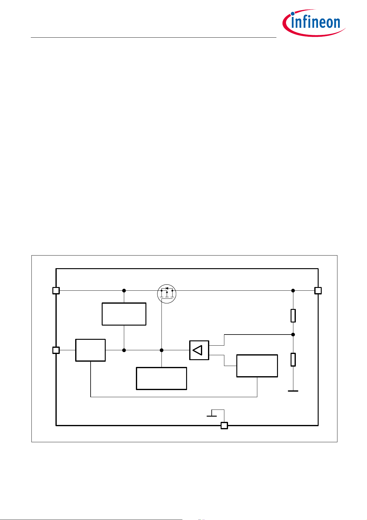
1.3 Block Diagram
Figure 1 shows the block diagram of TLS715B0NAV50.
Figure 1 Block Diagram of TLS715B0NAV50
User manual 4 Rev. 1.0
2019-09-24
Page 5

OPTIREG™ Linear TLS715B0NAV50 Demoboard
Z8F66967599
Demoboard
2 Demoboard
Figure 2 shows a TLS715B0NAV50 Demoboard.
Figure 2 TLS715B0NAV50 Demo Board
User manual 5 Rev. 1.0
2019-09-24
Page 6

OPTIREG™ Linear TLS715B0NAV50 Demoboard
Z8F66967599
Demoboard
2.1 Operating Conditions
To avoid any electrical damage of the Demoboard, the maximum operating range defined in Table 2 must be
followed.
Table 2 Operating Range
1)
Parameter Symbol Limit Values Unit Note
Min. Max.
Board Supply
2)
VIN 0 45 V Power supply
Regulator Output VOUT 0 7 V Regulated output voltage
Enable Signal EN 0 45
3)
V Enable signal to switch on the regulator
Ground GND 0 0 V System GND
1) The Demo Board operates at ambient temperature of 25°C.
2) Functional input voltage range starts from 4 V to 40 V.
3) Absolute max rating.
2.2 Board Configuration
The TLS715B0NAV50 Demoboard can be easily configured via jumpers on the board. The board provides the
following configuration options:
• Bypassing the reverse protection diode D2 via solder option SJ1
• Connecting enable signal with the supply voltage VIN (CON1)
• Placeholder for additional input capacitor (C2)
• Placeholder for additional output capacitor (C5)
• Placeholder for additional bulk input capacitor (C3)
• Placeholder for EN-input filter capacitance (C6)
User manual 6 Rev. 1.0
2019-09-24
Page 7

OPTIREG™ Linear TLS715B0NAV50 Demoboard
Z8F66967599
Demoboard
2.2.1 Enable Function
The jumper on the pin header JP_EN1 can be used to connect the EN signal to a external source via the
corresponding banana jack, or to GND, or to VIN. An overview of the different options is given in Table 3
“Jumper JP_EN1 setting for enable function” on Page 7.
Figure 3 Illustration of the two possible jumper positions
Table 3 Jumper JP_EN1 setting for enable function
JP_EN1 Enable Function
open EN is connected to the EN banana jack and can be driven by an external source
1)
Please consider placing C6 in this configuration to buffer EN when using long supply leads
Short pins 1,2 EN is connected to the supply voltage VIN; the regulator is enabled when it is supplied
Short pins 2,3 EN is shorted to GND and the regulator remains disabled
1) When no signal is applied externally, the regulator will remain disabled due to the internal pull-down resistor on EN
2.2.2 Signal Adaption
For easy signal adaption e.g. connecting probes for an oscilloscope, connectors TP_VIN, TP_I , TP_EN,
TP_VOUT and TP_GND can be used.
Table 4 Signals on connector
Connector Accessible Signals
TP_VIN - VIN (input voltage including reverse polarity protection diode)
TP_I - Regulator pin input voltage
TP_EN - EN (enable input signal)
TP_VOUT - VOUT (output voltage)
TP_GND - GND
User manual 7 Rev. 1.0
2019-09-24
Page 8

OPTIREG™ Linear TLS715B0NAV50 Demoboard
Z8F66967599
Schematic and Layout
3 Schematic and Layout
3.1 Schematic
Figure 4 Schematic of TLS715B0NAV50 Demoboard
3.2 Layout
Figure 5 Top Layer of TLS715B0NAV50 Demoboard
User manual 8 Rev. 1.0
2019-09-24
Page 9

OPTIREG™ Linear TLS715B0NAV50 Demoboard
Z8F66967599
Schematic and Layout
Figure 6 Bottom Layer of TLS715B0NAV50 Demoboard
Figure 7 Top Layer components of TLS715B0NAV50 Demoboard
User manual 9 Rev. 1.0
2019-09-24
Page 10

OPTIREG™ Linear TLS715B0NAV50 Demoboard
Z8F66967599
Bill of Material
4 Bill of Material
Table 5 Bill of Material
Part Value Package
VIN, VOUT, GND, EN Banana jack BABU4MM
C1 100 nF/50 V C0805
C2 n.p. (10 uF/50 V) C1206
C3 n.p. (47 uF/50V) E5-8,5
C4 1 uF/16 V C0805
C5 n.p. (10 uF/16 V) C1206
C6 n.p. (470 nF/50 V) C0805
CON1,JP_EN – 4/3 - pin header 2.54mm pitch
D1 SM4004 SMA
R1 0Ω R0805
R2 n.p. (100 kΩ) R0805
TP_EN,TP_GND,TP_I,TP_VIN,TP_V
OUT
SJ1 – solder jumper
D1 SM4004 diode
IC1 TLS715B0NAV50 PG-TSNP-7
– TEST POINT, KEYSTONE 5000
User manual 10 Rev. 1.0
2019-09-24
Page 11

OPTIREG™ Linear TLS715B0NAV50 Demoboard
Z8F66967599
General Information
5 General Information
5.1 Restrictions
This Demoboard is offering limited features allowing you only to evaluate and test the Infineon products. The
Demoboard is not an end product (or finished appliance), nor is it intended or authorized by Infineon to be
integrated into end products. You are not authorized to use the Demoboard in any production system.
5.2 Additional Information
• For further information you may contact http://www.infineon.com/
User manual 11 Rev. 1.0
2019-09-24
Page 12

OPTIREG™ Linear TLS715B0NAV50 Demoboard
Z8F66967599
Revision History
6 Revision History
Revision Date Changes
1.0 2019-09-24 Initial version.
User manual 12 Rev. 1.0
2019-09-24
Page 13

Trademarks of Infineon Technologies AG
All referenced product or service names and trademarks are the property of their respective owners.
IMPORTANT NOTICE
Edition 2019-09-24
Published by
Infineon Technologies AG
81726 Munich, Germany
© 2019 Infineon Technologies AG.
All Rights Reserved.
Do you have a question about any
aspect of this document?
Email: erratum@infineon.com
Document reference
Z8F66967599
The information contained in this application note is
given as a hint for the implementation of the product
only and shall in no event be regarded as a description
or warranty of a certain functionality, condition or
quality of the product. Before implementation of the
product, the recipient of this application note must
verify any function and other technical information
given herein in the real application. Infineon
Technologies hereby disclaims any and all warranties
and liabilities of any kind (including without limitation
warranties of non-infringement of intellectual
property rights of any third party) with respect to any
and all information given in this application note.
The data contained in this document is exclusively
intended for technically trained staff. It is the
responsibility of customer’s technical departments to
evaluate the suitability of the product for the intended
application and the completeness of the product
information given in this document with respect to
such application.
For further information on technology, delivery terms
and conditions and prices, please contact the nearest
Infineon Technologies Office (www.infineon.com).
WARNINGS
Due to technical requirements products may contain
dangerous substances. For information on the types
in question please contact your nearest Infineon
Technologies office.
Except as otherwise explicitly approved by Infineon
Technologies in a written document signed by
authorized representatives of Infineon Technologies,
Infineon Technologies’ products may not be used in
any applications where a failure of the product or any
consequences of the use thereof can reasonably be
expected to result in personal injury.
 Loading...