

Page 1

Application Note Please read the Important Notice and Warnings at the end of this document V 1.1
www.infineon.com page 1 of 54 2021-02-01
AN_1906_PL18_1908_180413
Scalable power inverter driving an electric
motor
Using the low voltage drives scalable power demonstration board
About this document
Scope and purpose
The low voltage drives scalable power demonstration board is a scalable platform for high power motor drive
applications. It has been developed to provide a flexible test environment for initial designs and technology
comparison. This document provides a detailed description of the platform modules, so the user will be able to
adapt the boards according to specific system requirements, and investigate and compare the capabilities of
power MOSFETs.
Intended audience
This document is intended for engineers using the "Low voltage drives scalable power demonstration board"
evaluation platform, or those evaluating the platforms suitability for use.
Table of contents
About this document ....................................................................................................................... 1
Table of contents ............................................................................................................................ 1
1 Introduction .......................................................................................................................... 3
2 Board overview ...................................................................................................................... 4
2.1 Power boards .......................................................................................................................................... 5
2.2 Master Mother Board and Mother Boards ............................................................................................ 10
2.2.1 Gate drivers option I – 2EDL23N06PJ .............................................................................................. 13
2.2.2 Gate drivers option II – 1EDN8550B ................................................................................................. 14
2.2.2.1 Functional principle of the 1EDN8550B (TDI) gate driver .......................................................... 15
2.2.2.2 Performance results with KIT_LGMB_BOM004 & KIT_LGMB_BOM504 ..................................... 16
2.3 Daughter boards .................................................................................................................................... 21
2.4 Functional principle of the 1EDN8550B (TDI) gate driver Capacitor boards ....................................... 22
2.5 Control board ........................................................................................................................................ 24
3 Three phase motor drive setup (B6) ......................................................................................... 25
3.1 Supply voltage ....................................................................................................................................... 26
3.2 Board interconnections in multiphase setups and power board paralleling ..................................... 26
3.2.1 Control signals – control board interface ........................................................................................ 27
3.2.2 Mother board bus ............................................................................................................................. 28
3.2.3 Daughter board bus ......................................................................................................................... 29
3.3 Using the V/f control for induction motor ............................................................................................ 29
3.3.1 Using the GUI .................................................................................................................................... 32
3.3.2 Driving an induction motor .............................................................................................................. 34
4 Performance of a B6 setup in a motor drive application ............................................................. 36
4.1 No paralleling ........................................................................................................................................ 37
4.1.1 Operating point 1 ............................................................................................................................. 38
4.1.2 Operating point 2 ............................................................................................................................. 40
4.2 Two per phase parallel connection ...................................................................................................... 42
Page 2

Application Note 2 of 54 V 1.1
2021-02-01
Scalable power inverter driving an electric motor
Using the low voltage drives scalable power demonstration board
Introduction
4.2.1 Operating point 3 ............................................................................................................................. 43
4.2.2 Operating point 4 ............................................................................................................................. 46
4.3 Four per phase parallel connection ...................................................................................................... 48
4.3.1 Operating point 5 ............................................................................................................................. 49
5 Summary ............................................................................................................................. 51
6 Reference ............................................................................................................................. 52
Revision history............................................................................................................................. 53
Page 3
Application Note 3 of 54 V 1.1
2021-02-01
Scalable power inverter driving an electric motor
Using the low voltage drives scalable power demonstration board
Introduction
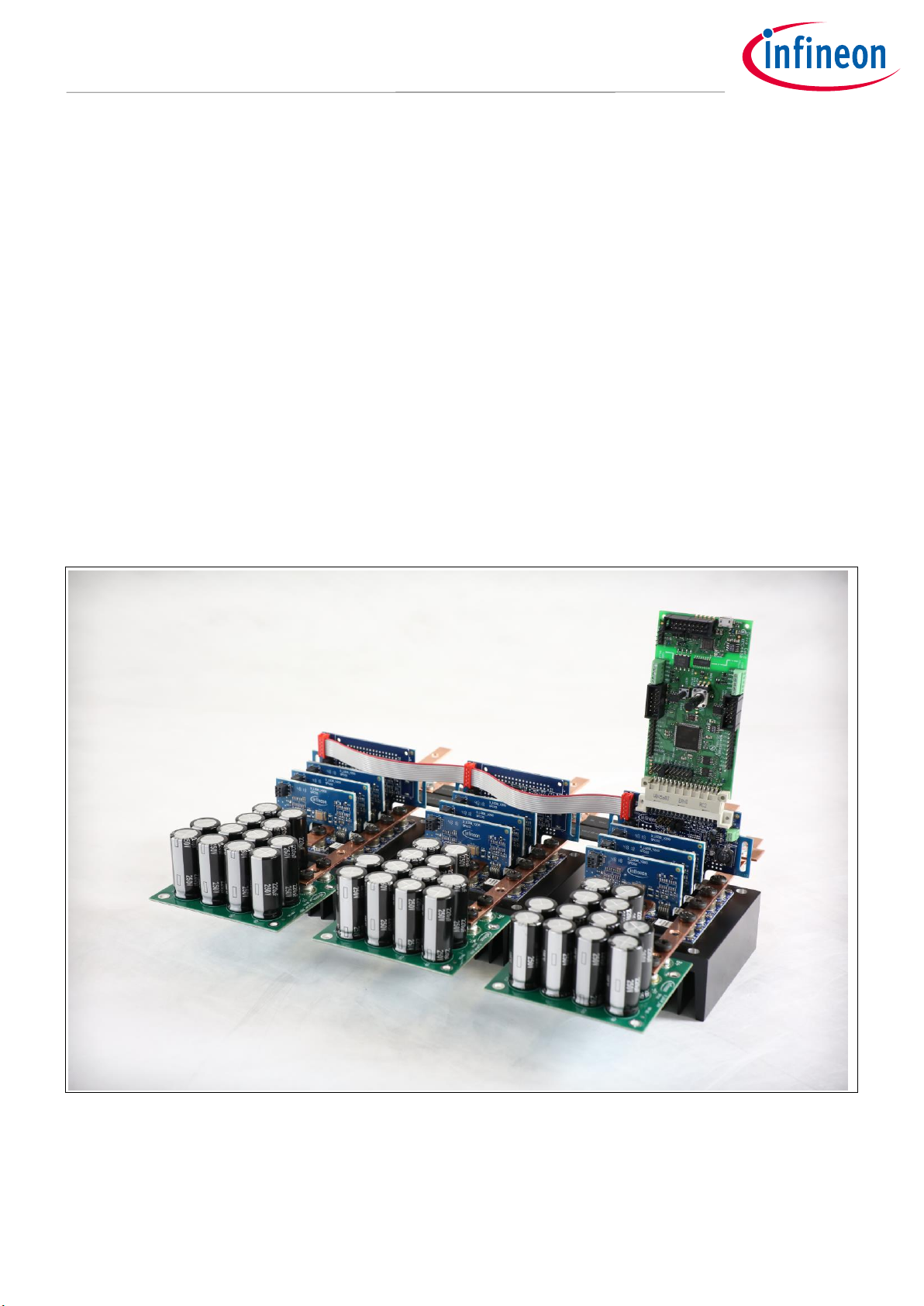
1 Introduction
The low voltage drives scalable power demonstration board offers the possibility of building a three-phase
motor drive setup of various power capabilities due to its MOSFET paralleling flexibility. The setup shown in
Figure 1 is an example of a three-phase inverter (also known as a B6 topology) for motor drive. The detailed
procedure of building such a setup is described in the “Low voltage drives scalable power demonstration board
user manual” [1].
The example is implemented with four MOSFETs connected in parallel in place of each B6 switch. The platform
was designed to be able to adapt the amount of MOSFET paralleling to the system requirements, by simply
adding or removing the power half-bridge modules. All components typically used for trimming performance
are located on FR4-based modules, while the power modules are implemented in IMS PCB technology adapted
to improve heat transfer using additional heatsinks – air-cooled or water-cooled.
This application note describes the details of the individual modules, their interconnection, and a graphical
user interface (GUI) complementing the supporting firmware. The aim is to provide the user with sufficient
knowledge to be able to utilize the modules in a working setup, and adapt the circuits to their own
requirements.
The examples provide a performance overview of the three-phase setup.
Figure 1 Typical setup for three-phase motor drive
Page 4
Application Note 4 of 54 V 1.1
2021-02-01
Scalable power inverter driving an electric motor
Using the low voltage drives scalable power demonstration board
Board overview
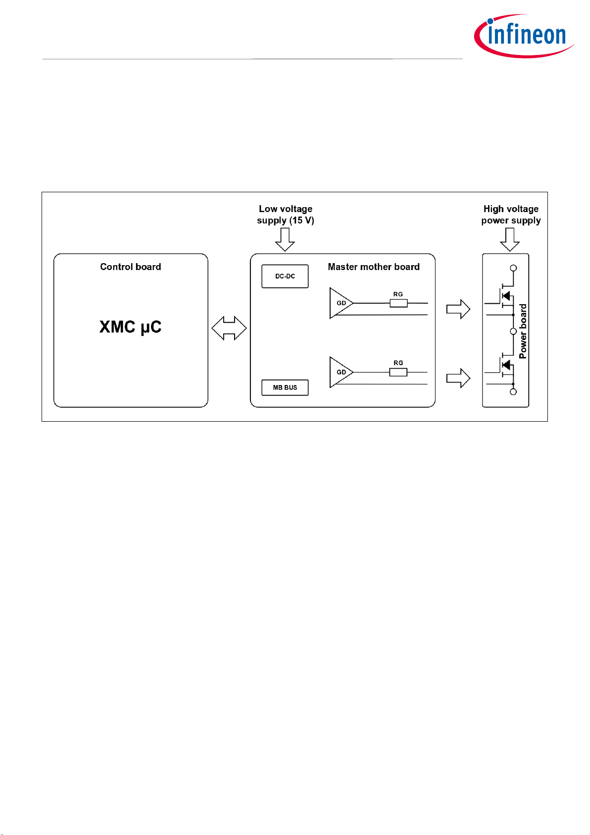
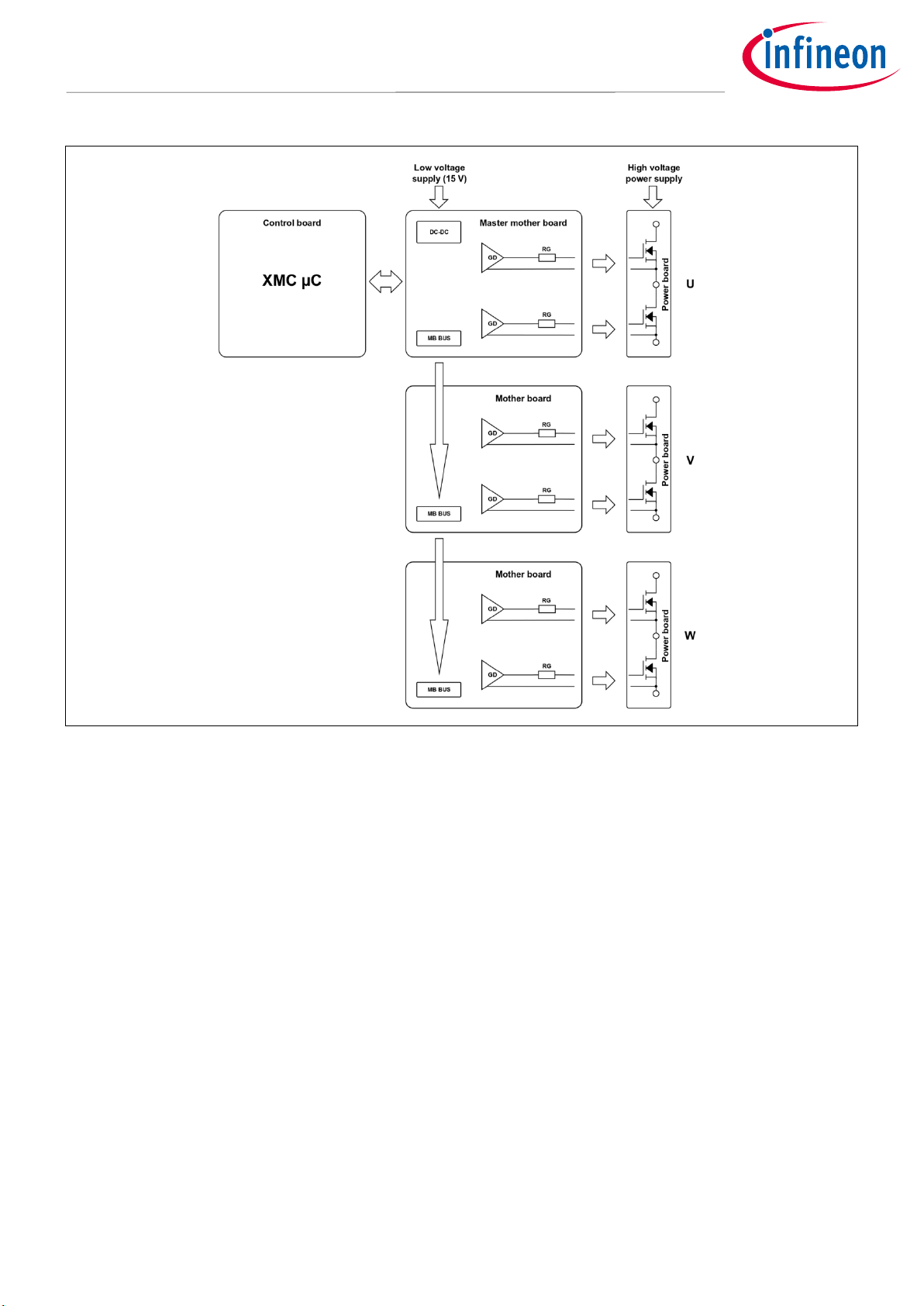
2 Board overview
The modular platform consists of different boards (modules) that can be used to design a fully functional
assembly, where each board has a specific role in a given setup. The modularity offers a wide range of possible
topologies. The concept supports half-bridge, full-bridge or three-phase topologies.
The basic principle of board functionality is illustrated in the block diagram in Figure 2.
Figure 2 Modular design – basic principles
By role (or functionality) in the setup, the modules are divided into five categories:
Power board: MOSFET half-bridge configuration
Mother board and master mother board: gate driver board – connects to the first paralleled power board
Daughter board: interconnection between the gate driver and the paralleled power boards
Capacitor board: PCB accommodating up to 12 capacitors connected to the DC bus
Control board: drive card XMC4400 demonstration board
Figure 2 shows a single-power half-bridge (power board), driven by the gate drivers (master mother board)
controlled by the XMCTM drive card (control board). Any setup is controlled by a control board (e.g. XMCTM drive
card – XMC4400) connected to the master mother board via the X3 connector.
The setup can be expanded to a multiphase setup using additional mother boards connected at the mother
board bus(MB bus) via a ribbon cable.
Each phase can be expanded with several power boards connected in parallel.
Page 5
Application Note 5 of 54 V 1.1
2021-02-01
Scalable power inverter driving an electric motor
Using the low voltage drives scalable power demonstration board
Board overview
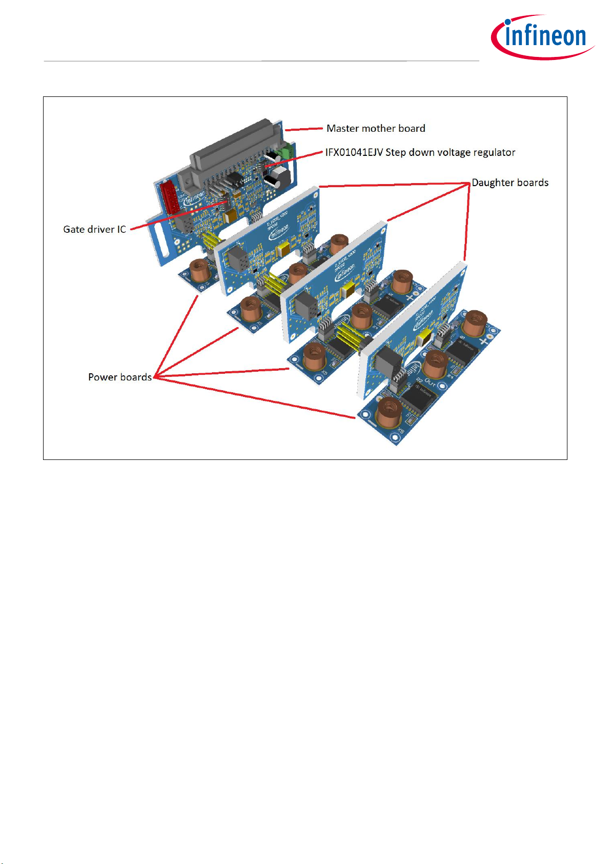
Figure 3 Single-phase assembly with paralleled power boards (exploded view)
Figure 3 shows an example of a single-phase (“U”) assembly with four power boards connected in parallel,
interconnected to the corresponding master mother board and three daughter boards.
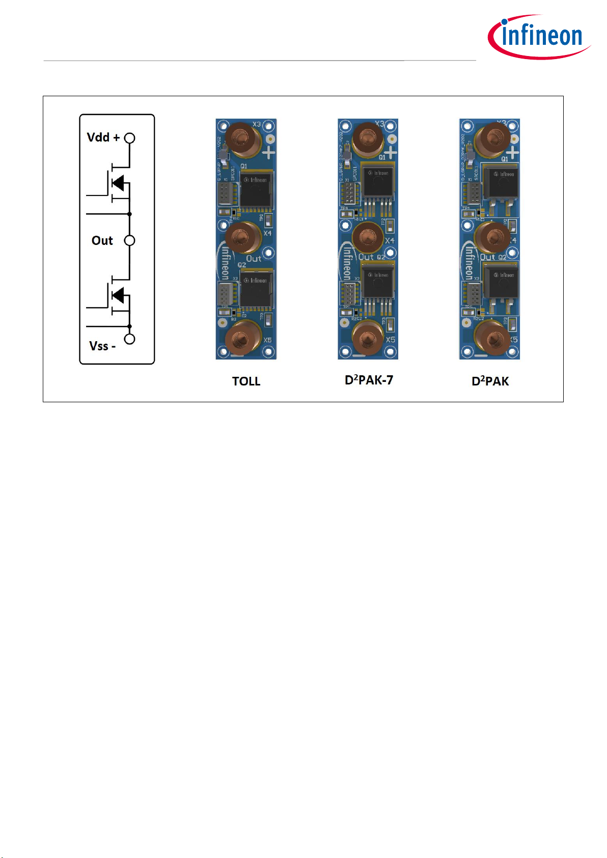
2.1 Power boards
The power boards are the main building blocks of the three-phase assembly. They are IMS PCB-based halfbridge sub-assemblies, comprising a single high-side (HS) and a single low-side (LS) MOSFET with all the
necessary connectors for power and signal lines.
Figure 4 shows the different versions of the power boards available.
Page 6
Application Note 6 of 54 V 1.1
2021-02-01
Scalable power inverter driving an electric motor
Using the low voltage drives scalable power demonstration board
Board overview
Figure 4 Power board versions: TOLL, D
2
PAK-7, D2PAK
Each board implements a different MOSFET package while maintaining the same interconnection layout, so
that all the different power board versions are interchangeable.
The featured packages are:
TO-leadless (TOLL)
D
2
PAK-7 (PG-TO263-7)
D
2
PAK (PG-TO263-2)
All available versions with regard to specific MOSFET products are provided online.
Page 7
Application Note 7 of 54 V 1.1
2021-02-01
Scalable power inverter driving an electric motor
Using the low voltage drives scalable power demonstration board
Board overview
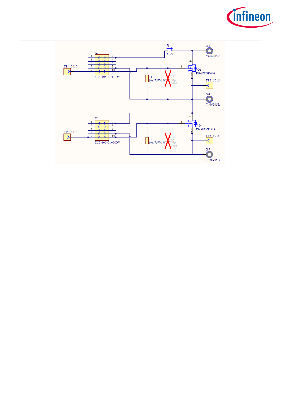
Figure 5 Power board schematic
The schematic shown in Figure 5 applies to all the power board versions. A number of test point connectors are
provided on the boards, since the platform is intended for test purposes.
The SMD connectors X3, X4 and X5 are provided for interconnection with high current capability. Either cable
lugs or copper bars can be used for the power connection to the connector via standard M5 screws.
Connectors X1 and X2 connect to the HS and LS MOSFETs respectively. All three MOSFET node (G, D, S)
connections are provided at the X1 and X2 connectors. The gate (G) and source (S) nodes connect to the gate
driver circuitry. Additionally, the HS drain (D) and the LS source (S) (i.e. the DC bus) are connected to a ceramic
capacitor located on the (master) mother boards or daughter boards via X1 and X2 connectors. The ceramic
capacitor provides the additional DC bus stability due to its proximity to the respective power board.
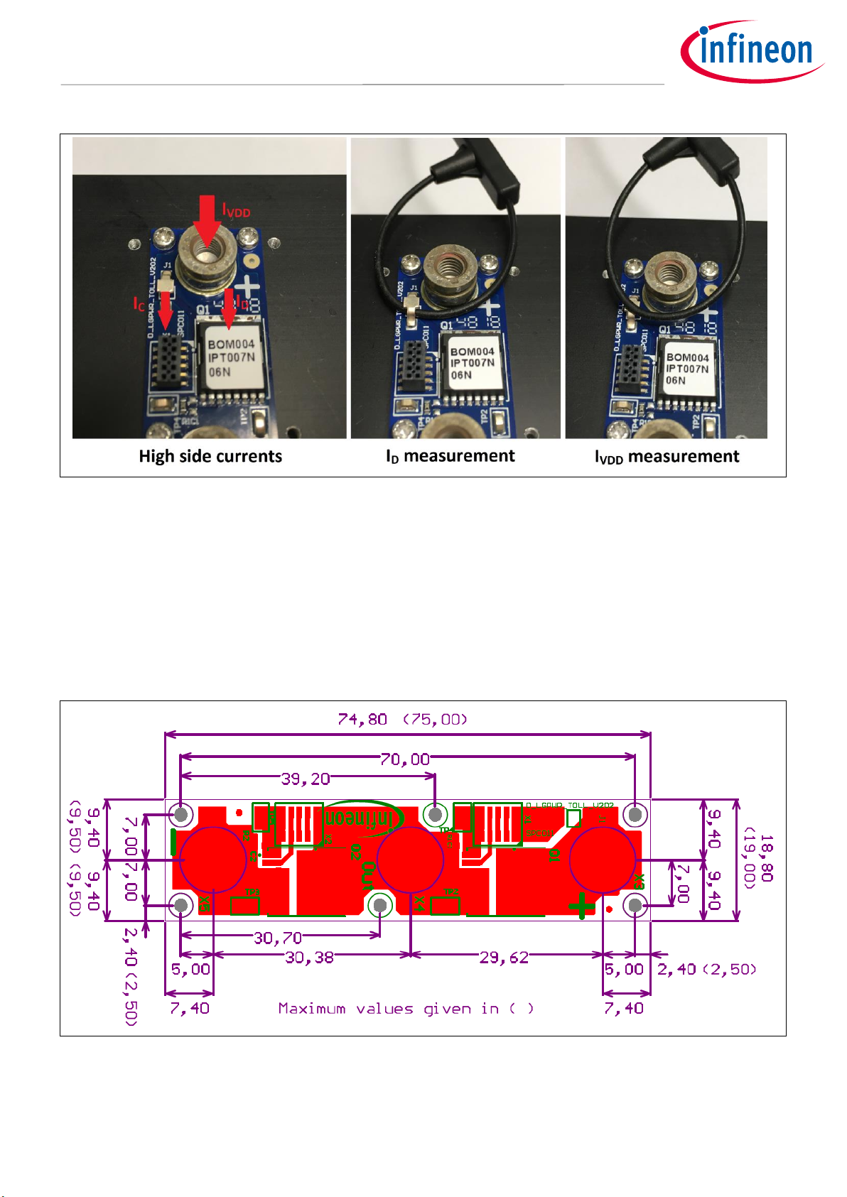
The test points (TP2, TP3, TP4, TP5) are small test hooks provided for connection of the oscilloscope probe clip.
The jumper (J1) provided at the HS drain (the VDD+ node) enables the user to utilize a Rogowski current probe
for HS MOSFET drain current measurements (ID), as demonstrated in Figure 6. The current I
VDD
flowing from the
DC power supply V
DD+
through the X3 power terminal is split between the MOSFET drain current ID, and IC
(current flowing to the capacitor through X1). Considering that the capacitor current IC is flowing through the J1
jumper, the user can choose between measuring ID (Rogowski coil enclosing X3 and J1) and I
VDD
(Rogowski coil
reaching around X3 and above J1).
Page 8
Application Note 8 of 54 V 1.1
2021-02-01
Scalable power inverter driving an electric motor
Using the low voltage drives scalable power demonstration board
Board overview
Figure 6 Rogowski probe for measuring HS I
D
or I
VDD
2.1.1 Power board PCB layout
The IMS boards are intended to be attached to a heatsink via six M2 screws. To prepare the threaded holes in
the heatsink consider the dimensions in Figure 7. The placement of the screw holes and the power connectors
are the same for all the power board versions of the modular platform.
When machining the copper bars for the power connections, 19 mm spacing between the screw holes is
recommended.
Figure 7 Power board layout and dimensions
Page 9
Application Note 9 of 54 V 1.1
2021-02-01
Scalable power inverter driving an electric motor
Using the low voltage drives scalable power demonstration board
Board overview
2.1.2 IMS board and heatsink
The power boards use the Ventec VT-4B3 IMS type. Table 1 lists some of the main properties.
Table 1 IMS board details
Description
Dimension
Substrate thickness
1.4 mm
Dielectric thickness
100 µm
Copper thickness
105 µm
Overall board thickness
1.6 mm
Dielectric specific thermal conductivity λ [W/m*K]
3 W/(m*K)
2.1.3 Board assembly and X-ray investigation of the power boards
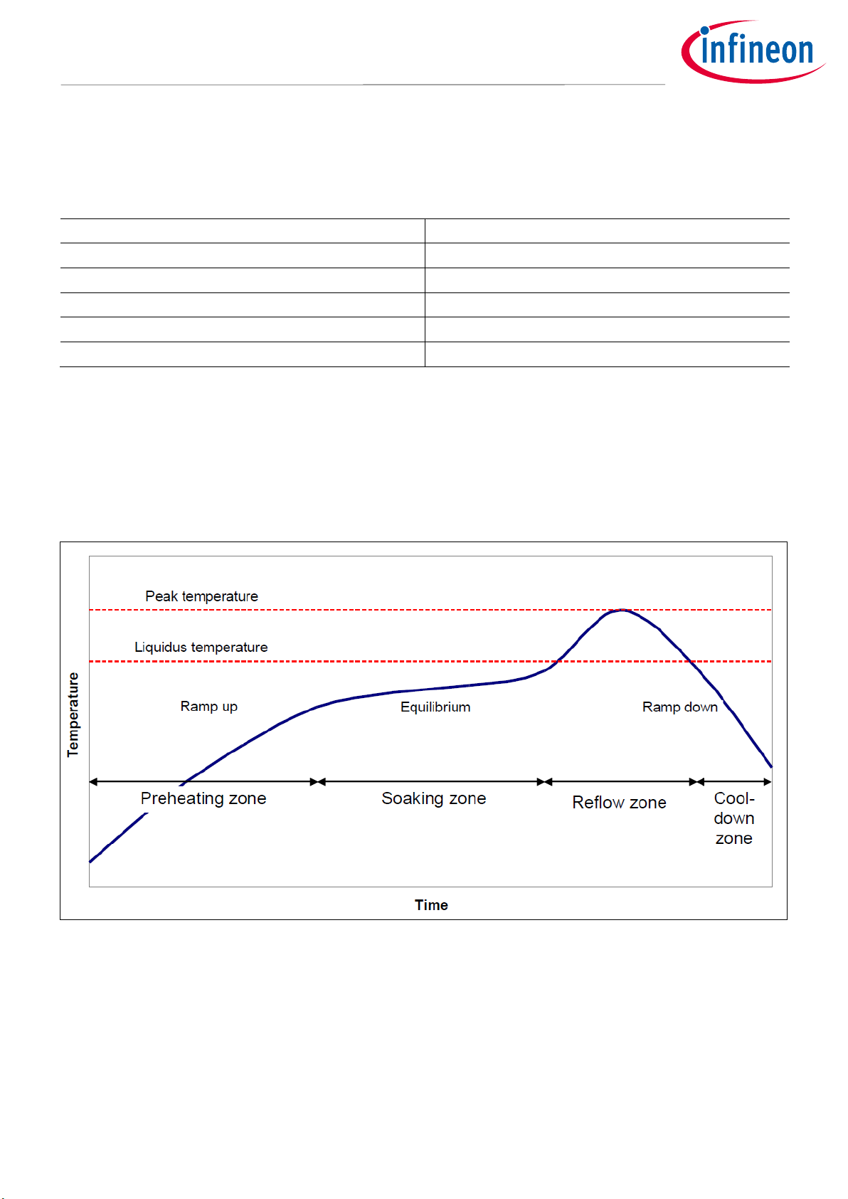
The soldering method used for the IMS board assembly was vapor phase soldering. The temperature profile of
this process is similar to the standard reflow process, with the peak temperature of the process at 250°C
defined by the phase change temperature of the inert liquid being used. The reflow zone time interval was 3
minutes.
Figure 8 Temperature profile [2]
Further details and recommendations for assembly of Infineon packages are available online [2].
X-ray imaging was used to inspect the quality of the soldering process. The result is shown in Figure 9. A certain
number of voids are to be expected and can only be eliminated using a more advanced process of reflow
soldering in vacuum. However, the images show a fairly successful result with voids representing less than 10
percent of the soldered surface area.
Page 10
Application Note 10 of 54 V 1.1
2021-02-01
Scalable power inverter driving an electric motor
Using the low voltage drives scalable power demonstration board
Board overview
Figure 9 X-ray inspection – voids between lead-frame and PCB
2.2 Master mother board and mother boards
The master mother board and the mother board shown in Figure 10 provide the gate drivers for the HS and LS
MOSFETs for each of the half-bridges, as shown in Figure 11.
Figure 10 Master mother board and mother board
Page 11
Application Note 11 of 54 V 1.1
2021-02-01
Scalable power inverter driving an electric motor
Using the low voltage drives scalable power demonstration board
Board overview
Figure 11 Utilization of master mother board and mother boards in multiphase setups (e.g. U, V, W)
The difference between the two is in the connection to the XMCTM control board. The control board connects to
the master mother board, and the signals to the mother boards are propagated via the mother board bus.
Mother boards are only used alongside the master mother board when a two- or three-phase system is
implemented, as shown in Figure 11.
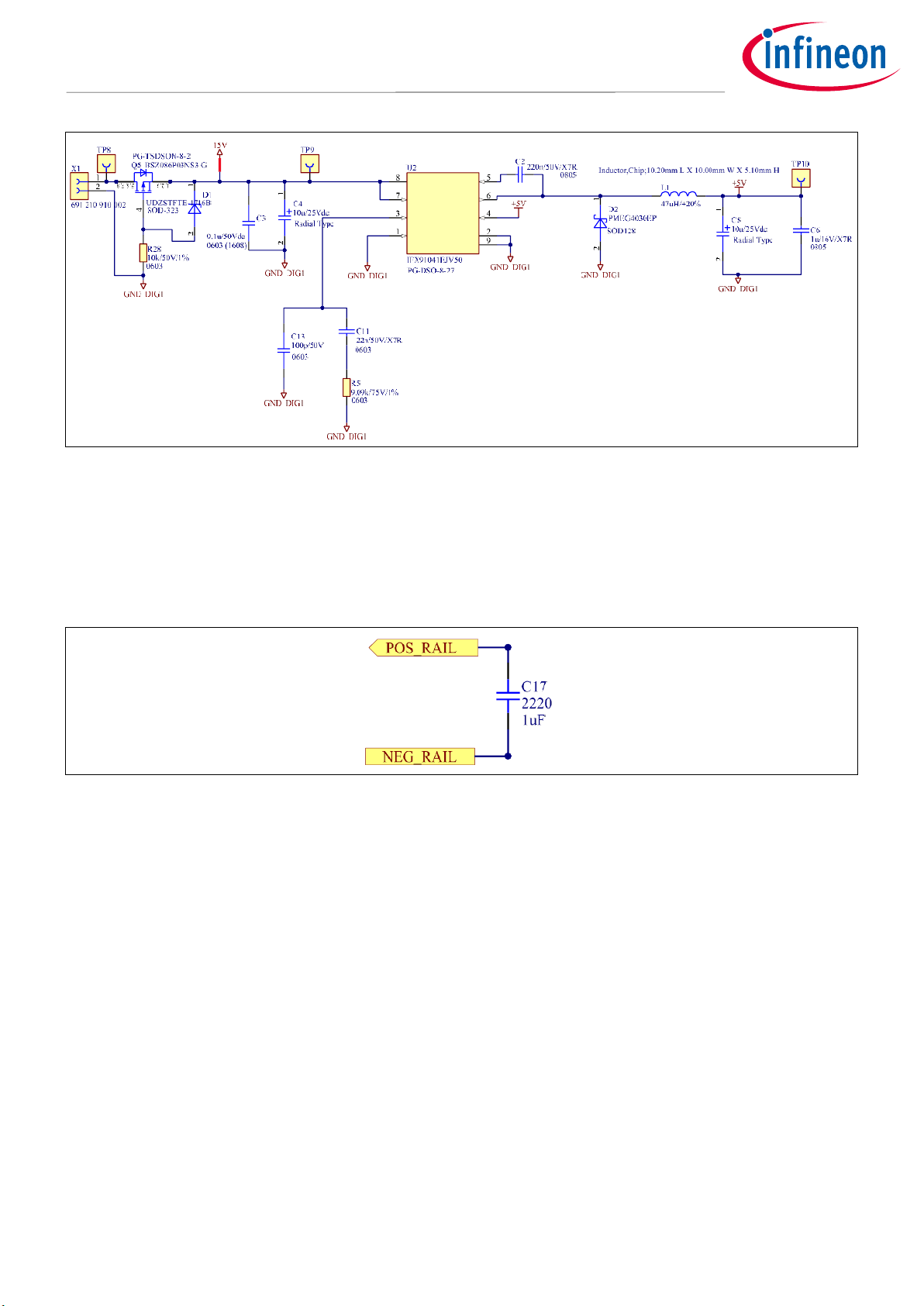
The master mother board also includes the onboard power supply sub-circuit that provides the 5 V supply line
powering the XMCTM control board. The 15 V supply for the gate drivers is propagated via the mother board bus
to the mother boards.
System supply
Note: The master mother board must be supplied from an external 15 V power source (at the X1
connector teminal).
The onboard IFX91041EJV50 generates the 5 V supply.
Page 12
Application Note 12 of 54 V 1.1
2021-02-01
Scalable power inverter driving an electric motor
Using the low voltage drives scalable power demonstration board
Board overview
Figure 12 15 V to 5 V converter (master mother board)
DC bus ceramic capacitors
The master mother board and the mother boards provide a ceramic capacitor C17(c) connected to the high
voltage DC bus through the X2 and X5 headers. The intention is to provide the low ESR capacitors as close as
possible to each of the power boards in order to stabilize the DC bus voltage.
Figure 13 DC bus capacitor
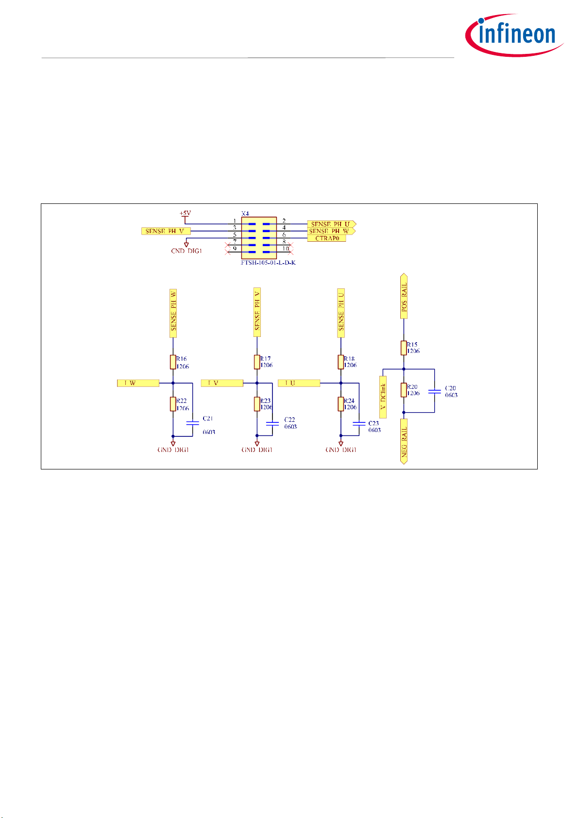
Current sensor connection
The X4 connector on the master mother board, enables the user of optionally connecting voltage nodes or
current sensors, to the microcontroller analog inputs. The subcircuit is shown in Figure 14
A Samtec FTSH-105-01-L-D-K header connector can be used in place of the X4 connector to interface the
external sensors. The voltage dividers need to be adjusted according to the sensor output voltage range, and
the filtering capacitors to the required frequency range. The pins on X4 are intended to connect to the external
nodes while the nodes leading to the XMCTM inputs through the X3 connector are:
I_U
I_V
I_W
V_DClink
Page 13
Application Note 13 of 54 V 1.1
2021-02-01
Scalable power inverter driving an electric motor
Using the low voltage drives scalable power demonstration board
Board overview
The connection of two-phase current sensors enables the current limit feature in the GUI (described in chapter
3.3). The feature uses the two-phase currents to calculate the current vector amplitude and compares it to the
current limit set in the GUI.
In order to enable the feature, the current sensors need to be connected to:
SENSE_PH_U (X4 - pin 2)
SENSE_PH_W (X4 - pin 4)
Figure 14 Current sensor connection
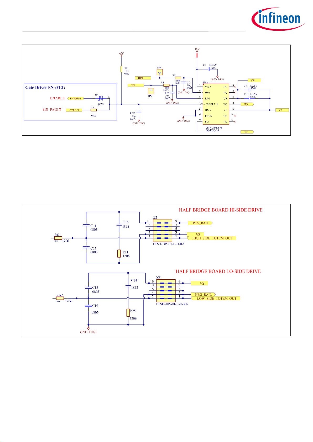
2.2.1 Gate drivers option I – 2EDL23N06PJ
KIT_LGMB_BOM003 & KIT_LGMB_BOM503
The 2EDL family gate drivers feature integrated HS and LS gate drivers, with an integrated bootstrap diode. The
gate driver output signals are propagated to the power board through header connectors X2 and X5. Mother
boards also include the gate resistors (RG1, RG2) for the two MOSFET gates connected at X2 and X5.
The default populated gate resistor (RG1 and RG2) values are 47 Ω. This value is suitable to be used with most
of the MOSFETs; however, it is not to be considered an optimum value. The intention of the platform is to
provide the option to easily change the RG values and adapt them to specific application requirements.
Page 14
Application Note 14 of 54 V 1.1
2021-02-01
Scalable power inverter driving an electric motor
Using the low voltage drives scalable power demonstration board
Board overview
Figure 15 Mother board implementation of 2EDL23N06PJ
In addition to the gate resistors, the board offers the possibility to connect additional capacitors between the
MOSFET terminals (G-S, G-D, D-S), as shown in Figure 16 for the HS and LS MOSFETs (refer to Figure 5 for power
board connections). This enables even greater influence on switching behavior optimization.
The components (C14, C15, C16, R11, C18, C19, C24, R25) are not populated by default. Only the PCB footprints
are available for the user to utilize according to project requirements.
Figure 16 Power board interface – MOSFET interconnection
2.2.2 Gate drivers option II – 1EDN8550B
KIT_LGMB_BOM004 & KIT_LGMB_BOM504
The pin-outs of the external connections are functionally the same in both options to accommodate
interchangeablity of the mother boards in the overall system. Other than some layout improvements, the
differences between the options are associated with the gate driver specifics.
Page 15
Application Note 15 of 54 V 1.1
2021-02-01
Scalable power inverter driving an electric motor
Using the low voltage drives scalable power demonstration board
Board overview
Figure 17 Mother board implementation of 1EDN8550B
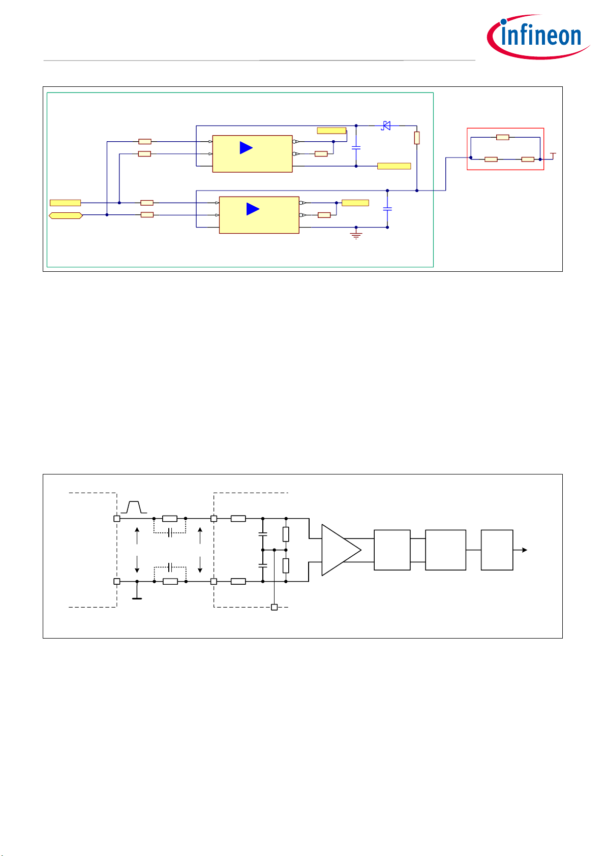
2.2.2.1 Functional principle of the 1EDN8550B (TDI) gate driver
The EiceDRIVER™ 1EDN8550B is a single-channel non-isolated gate driver with truly differential inputs (TDI) [3].
This concept for the input side of the gate driver makes it able to overcome the driving issues when a DC
ground-shift or an AC oscillation exists between the microcontroller and the driver IC ground potentials.
Common situations characterized by DC and AC ground-shifts are, for example, driving a HS switch in a halfbridge configuration, or driving in noisy environments with significant stray inductance on the ground path.
Some interesting use cases can be found in industrial, server and telecom SMPS as well as motor drive, wireless
charging applications, home appliances, power tools and solar micro-inverters. Figure 18 represents the
functional principle of the TDI gate driver and how it should be connected to the controller in order to
effectively prevent false triggering of the power switches.
IN+
IN-
Differential
Schmitt
Trigger
Av = 4.5
12 MHz
2nd order
Lowpass
Controller
PWM
SGND
0
R
in1
R
in2
2kW
2kW
1kW
1kW
15pF
15pF
1EDN8550
GND
Pulse
Extender
C
p2
C
p1
VS 5V
DV
Rin
DV
Rin
/ k
k = (R
in
[kW] + 3) / 3 = (51 + 3) / 3 = 18
51kW
51kW
Figure 18 Functional principle of the single-channel non-isolated gate driver with TDI
The controller PWM output signal, switching between controller supply voltage (VS) and zero, is applied on one
leg of a differential voltage divider, while the other is connected to the controller ground SGND. The divider
ratio has to be adapted to VS to allow a fixed Schmitt trigger threshold voltage. For VS = 5 V, R
in1
and R
in2
are
chosen to be 51 kΩ (see Table 1 [4]), resulting in a static divider ratio of k = 18 at the driver inputs. Taking into
account the resistor-capacitor (RC) filter in front of the internal voltage amplifier, the overall input path exhibits
the frequency behavior of a third-order low-pass filter with a corner frequency around 12 MHz. The suppression
of high frequencies is important for two reasons. Inductive common-mode (CM) ringing in fast-switching power
systems is typically in the 100 MHz and above range, and thus is effectively damped. The high-frequency
symmetry of the voltage divider is influenced by parasitic capacitances, particularly Cp1 and Cp2, the parallel
HO
LO
PHASE
HO
LO
1 2
D3
S100
HIN
LIN
HINGD
LINGD
0603
R2
1R/1%
0603
R4 33k/0.1%
0603
R8 33k/0.1%
HIN
LIN
When HIN and LIN max 3.3V then R1,R3,R4,R8=33k, 0603, 0.1% (PHASE voltage limited to 84V)
PGND
1206
Rp3
0R
+15V
RG3
4.7R
VDD
4
IN_P
3
IN_N
1
OUT_SNK_N
6
GND
2
OUT_SRC_N
5
U1
1EDN8550B
VDD
4
IN_P
3
IN_N
1
OUT_SNK_N
6
GND
2
OUT_SRC_N
5
U3
1EDN8550B
0R 1206
Rp2
22u/25V/X5R
1206
C12
4.7u/25V/X7R
1206
C9
Use 20x MOSFET input capacitance for Bootstrap capacitor
RG4
4.7R
0603
R1
33k/0.1%
0603
R3
33k/0.1%
Rp1
0R 1206
Page 16

Application Note 16 of 54 V 1.1
2021-02-01
Scalable power inverter driving an electric motor
Using the low voltage drives scalable power demonstration board
Board overview
capacitances of R
in1
and R
in2
. They are typically in the 50 to 100 fF range, independent of resistor size. Without
filtering, any asymmetry would translate high-frequency CM signals into differential signals. The filtered signal
is then applied to a differential Schmitt trigger with accurate trimmed threshold levels and converted to the
logic switch control signal. The subsequent pulse extender function guarantees that no pulses shorter than 25
ns are transmitted to the output, thereby further improving noise immunity. Due to the filtering requirements,
the input-to-output propagation delay is slightly increased to around 45 ns. By means of on-chip trimming,
however, the usually more relevant propagation delay variation can still be kept low at +10/-7 ns.
The static voltage range at the input pins is limited to -7 V/+6 V to guarantee accurate linear operation of the
input circuitry. Any imbalance in the signal path converts a CM signal to a differential signal. To utilize the full
CM range as calculated above, the high accuracy of the trimmed on-chip network must not be affected by the
external voltage divider resistors. This condition is easily fulfilled when choosing R
in1
and R
in2
with 0.1 percent
tolerance. However, the power rating and the size of the external resistor pair play an important role as
“bottleneck” to achieve high DC and AC ground-shift robustness. In this case, a 1206-size resistor has been
selected to ensure a proper creepage and clearance at the PCB level. Since the 51 kΩ/0.1 percent/1206 resistors
available in the market are typically rated 200 V, the static CMR of the driving configuration in Figure 18 is
limited to the range of -126 V/+108 V.
Benefits:
Immunity to interference
Decoupling of signal and power GND
2.2.2.2 Performance results with KIT_LGMB_BOM004 and KIT_LGMB_BOM504
The key components used in this setup to conduct the following gate driver tests are:
1. Driver IC (mother board) – 1EDN8550B (EiceDRIVER
TM
)
2. MOSFET (power board) – IPB017N10N5 (OptiMOS
TM
)
3. Controller (controller card) – XMC4400 (XMC
TM
)
High dv/dt immunity:
This section highlights the ripple noise between the signal ground and power ground and on high dv/dt of the
output node. The setup was designed to create the worst-case conditions for switching. As the objective is to
measure the ripple noise, the double pulse testing method is used instead of continuous switching. The
switching speed for turn-on and turn-off are swept by changing the value of external gate resistance (Rg) in
steps to reach the harsh conditions described above with high output dv/dt, high di/dt of ID and high groundshift ripples.
Page 17
Application Note 17 of 54 V 1.1
2021-02-01
Scalable power inverter driving an electric motor
Using the low voltage drives scalable power demonstration board
Board overview
Inductive
Load
C_Bank
48V
DC
U W
C_Bank
TDI
HS
TDI
LS
TDI
HS
TDI
LS
V
DD
V
DD
V
DD
V
DD
Ground Shift (LParasitic)
Positive Rail
Negative Rail V
U_GND
V
W_GND
x 4 x 4
Figure 19 Ground-shift realization in HB/FB applications
The microcontroller ground is only connected to a single point in the circuit (in this case V
U_GND
). The voltage
difference between the signal ground (V
U_GND
→ SGND) and power ground (V
W_GND
→ PGND) is a result of induced
voltage in the L
parasitic
, as shown in Figure 19. The switching properties (output dv/dt, ID di/dt) are shown in Table
2. The noise produced in the system, measured as the oscillation of the ground-shift, varies with a high peak-topeak amplitude of 14.24 V and lasts for less than five cycles (less than 12 µs) of decreasing magnitude, and is
within the CMR of TDI driver IC.
Table 2 Switching speed measurements of test setup
Measurement parameter
Turn-off
Turn-on
Switch-node dv/dt
350 V/µs
4200 V/µs
Drain current diD/dt (A/µs)
800 A/µs
900 A/µs
Voltage PGND vs. SGND dv/dt (V/µs)
65 V/µs
33 V/µs
Voltage PGND vs. SGND amplitude (pk-pk)
14.24 V
14.24 V
Page 18

Application Note 18 of 54 V 1.1
2021-02-01
Scalable power inverter driving an electric motor
Using the low voltage drives scalable power demonstration board
Board overview
Figure 20 Ground-shift between signal ground and power ground
The difference in potentials between the signal (µC) ground and power ground (i.e. ground-shift) shown in
Figure 20 represent the CM voltage of the LS differential input, and the switch-node voltage represents the HS
differential input. In both cases the CM is not influencing the gate driver input, and high-frequency CM voltages
(ringing) greater than 333 kHz are further dampened by the input low-pass filter. In such fast-switching
situations, the high robustness of 1EDN8550B with respect to switching interference is extremely valuable and
allows good performance even in systems with significant parasitic PCB inductances.
The ground-shift problem in specific applications can be addressed by Infineon’s TDI gate driver IC, and in the
same way, the TDI can handle the voltage offset and high dv/dt of a bootstrapped gate driver.
Gate driver supply filter:
This section descibes the optimization of the input filter for the gate driver supply side. Usually SGND-coupled
VDD cannot be used directly as the driver supply due to the high ripples of ground-shift. The filter can be a
simple resistor or a resistor in series with a diode, or series and parallel combinations of these components
together with the decoupling capacitor (C12) as indicated in Figure 17 (Rp1, Rp2, Rp3). The filter can also be a
proper ferrite bead depending on application and cost requirements. To choose the filter components
optimally, the LVDSPD setup has been continuously switched in worst-case conditions described above with a
DC current flowing in an R-L load.
The test specifications are:
GD supply: V
DD
= 15 V
Switching frequency: f_PWM = 20 kHz
Duty cycle: D = 11 percent
Load current: I_L = 210 A
Drain current I
D
: di/dt = 900 A/µs (Rg1 = 15 Ω, Rg3 = 10 Ω)
Switch-node voltage V
(SW)
: dv/dt more than 4000 V/µs
The variations to the test setup are:
Page 19

Application Note 19 of 54 V 1.1
2021-02-01
Scalable power inverter driving an electric motor
Using the low voltage drives scalable power demonstration board
Board overview
Only R filter
Only diode
Diode with resistors
Figure 21 shows:
The switch-node voltage
TDI driver IC supply voltage seen across bypass capacitor C12 (last combination of values – diode with
resistors)
The ripple voltage at the filter input
Figure 21 Ripple across gate driver input supply
The filter components comprise Rp1, Rp2 and Rp3 – 1206 footprint (Figure 17). Changing these components
results in different thermal situations and different resulting voltages on C12. The results for a few value
combinations are shown in Table 3. The temperatures recorded from images captured by thermal camera are
shown in Figure 22 for the optimized filter (Rp1 = diode, Rp2 = 10 Ω, Rp3 = 47 Ω). Please note that both the
driver ICs are cooler than 50°C. The rest of the board does not get significantly hot.
Figure 22 Thermal captures of filter section
Page 20

Application Note 20 of 54 V 1.1
2021-02-01
Scalable power inverter driving an electric motor
Using the low voltage drives scalable power demonstration board
Board overview
Table 3 Measurement parameters of optimized filter section
Measurement
Rp1 = n.p.
Rp2 = n.p.
Rp3 = 15 Ω
Rp1 = n.p.
Rp2 = n.p.
Rp3 = diode
Rp1 = diode
Rp2 = 10 Ω
Rp3 = 22 Ω
Rp1 = diode
Rp2 = 10 Ω
Rp3 = 47 Ω
Voltage PGND to SGND (pkpk)
19.0 V
18.7 V
19.1
20.98 V
Voltage VC12 (mean)
14.63 V
19.65 V
15.16 V
15.32 V
Temperature of filter
components
(Rp1, Rp2, Rp3)
84.2°C
43°C
38.9°C
54.3°C
67.4°C
36.81°C
50.9°C
48.7°C
Temperature of C12
43.1°C
44.6°C
54.3°C
33.1°C
Temperature of PCB
38°C
38.6°C
30.2°C
30.9°C
Temperature of LS GD (U3)
46.1°C
51.6°C
38.4°C
37°C
Temperature of HS GD (U1)
49°C
62.1°C
40.1°C
38.5°C
The results in Table 3 indicate the preferred combination of components as:
Rp1 = diode (SBD – SS14L SMA 1 A 40 V, V
f
= 0.196 V),
Rp2 = 10 Ω and
Rp3 = 22 Ω or 47 Ω
However, in a system with less ripple other combinations are also acceptable, and may simplify the design.
Gate driver output loading:
This section estimates the loading on the gate driver by emulating the MOSFETs by R and C components (Figure
23). The switching frequency of the PWM is set at 20 kHz.
The test setup values are:
Capacitive load: C
L
= 210 nF (0805)
GD supply: V
DD
= 15 V
External gate resistance: R
g
a. R
g2
= 0 Ω; Rg4 = 4.7 Ω, 2.2 Ω and 1 Ω
b. R
g2
= 15 Ω, Rg4 = 10 Ω
12V
55k
55k
SGND
VRin
IN-
GND
IN+
OUT_SNK
OUT_SRC
VDD
CVDD
1EDN8550B
CL
Controller
SGND
PWM_Out
Rg4
Rg2
Figure 23 Schematic for gate driver output loading
Page 21

Application Note 21 of 54 V 1.1
2021-02-01
Scalable power inverter driving an electric motor
Using the low voltage drives scalable power demonstration board
Board overview
The source and sink resistances in this case will be Rg2 + Rg4 and Rg2 respectively. The power dissipation in the
gate driver heats up the IC and the temperatures are recorded with a thermal camera. The recorded data is
shown in Table 4.
Table 4 Gate driver output loading measurements
f_PWM (kHz)
Rg (Ω)
Temperature (T) (°C)
IC-U3 (°C)
Rg4 (°C)
Rg2 (°C)
20 kHz
Rg2 = 0 Ω, Rg4 = 4.7 Ω
64.5
79.8
–
Rg2 = 0 Ω, Rg4 = 2.2 Ω
66.4
68.6
–
Rg2 = 0 Ω, Rg4 = 1 Ω
76.3
61.7
–
Rg2 = 15 Ω, Rg4 = 10 Ω
40.2
55.3
89
The data from the Table 4 shows the application of the TDI gate driver for different switching speed
applications and temperature limitation problems. Depending on the values of Rg2 and Rg4, the parts of the IC
that represent the sourcing output and sinking output may be at different temperatures.
2.3 Daughter boards
Daughter boards are used for the interconnection between the gate driver outputs and power boards (MOSFET
gates) via X7 and X11 header connectors, when adding power boards in parallel.
Figure 24 Daughter board
Typically, MOSFETs connected in parallel are driven by a single gate driver, while the gate resistors (RG) are
provided for each MOSFET gate. The gate driver signal branches out at the gate driver output – before the RG
resistors and not at the gate nodes. The daughter boards are therefore connected to the gate driver outputs at
one side (forming the daughter board bus – Chapter 3.2.3), and to the MOSFET gate and source connection at
the other side (Figure 5). Each daughter board provides each additional power board with the respective HS
and LS gate resistors. The principle is illustrated in Figure 25.
Page 22

Application Note 22 of 54 V 1.1
2021-02-01
Scalable power inverter driving an electric motor
Using the low voltage drives scalable power demonstration board
Board overview
Figure 25 Paralleling approach
2.3.1 Power board interface
At the point of connection to the power board, the same optional components are available as in the mother
boards. The schematic is shown in Figure 16 and Figure 13. The ceramic capacitor C17(c) is populated by
default.
2.4 Functional principle of the 1EDN8550B (TDI) gate driver capacitor
boards
The capacitor boards provide the option to connect leaded capacitors to the high-power DC bus. The highcurrent connectors have the same spacing as the power board DC bus connectors. This way the copper bars
can be extended in order to make the low parasitic inductance connection between the power board and the
capacitor board.
Figure 26 Capacitor board
Page 23

Application Note 23 of 54 V 1.1
2021-02-01
Scalable power inverter driving an electric motor
Using the low voltage drives scalable power demonstration board
Board overview
The capacitor boards are populated with power connectors only. This way the user can select the capacitors
according to project requirements.
It is recommended to use capacitors with low ESR values.
Table 5 Capacitor selection size requirements
Parameter
Values
Unit
Min.
Typ.
Max.
Capacitor diameter
18
mm
Lead spacing
7.5 mm
Figure 27 Capacitor board dimensions
Attention: Normally the bus capacitors are discharged when the lab power supply is switched off. But if
the power connector is removed while the capacitor is charged (not recommended!), the
voltage preserved at the bus capacitors can reach a dangerous level. Be sure that capacitors
are discharged before handling the board.
Page 24

Application Note 24 of 54 V 1.1
2021-02-01
Scalable power inverter driving an electric motor
Using the low voltage drives scalable power demonstration board
Board overview
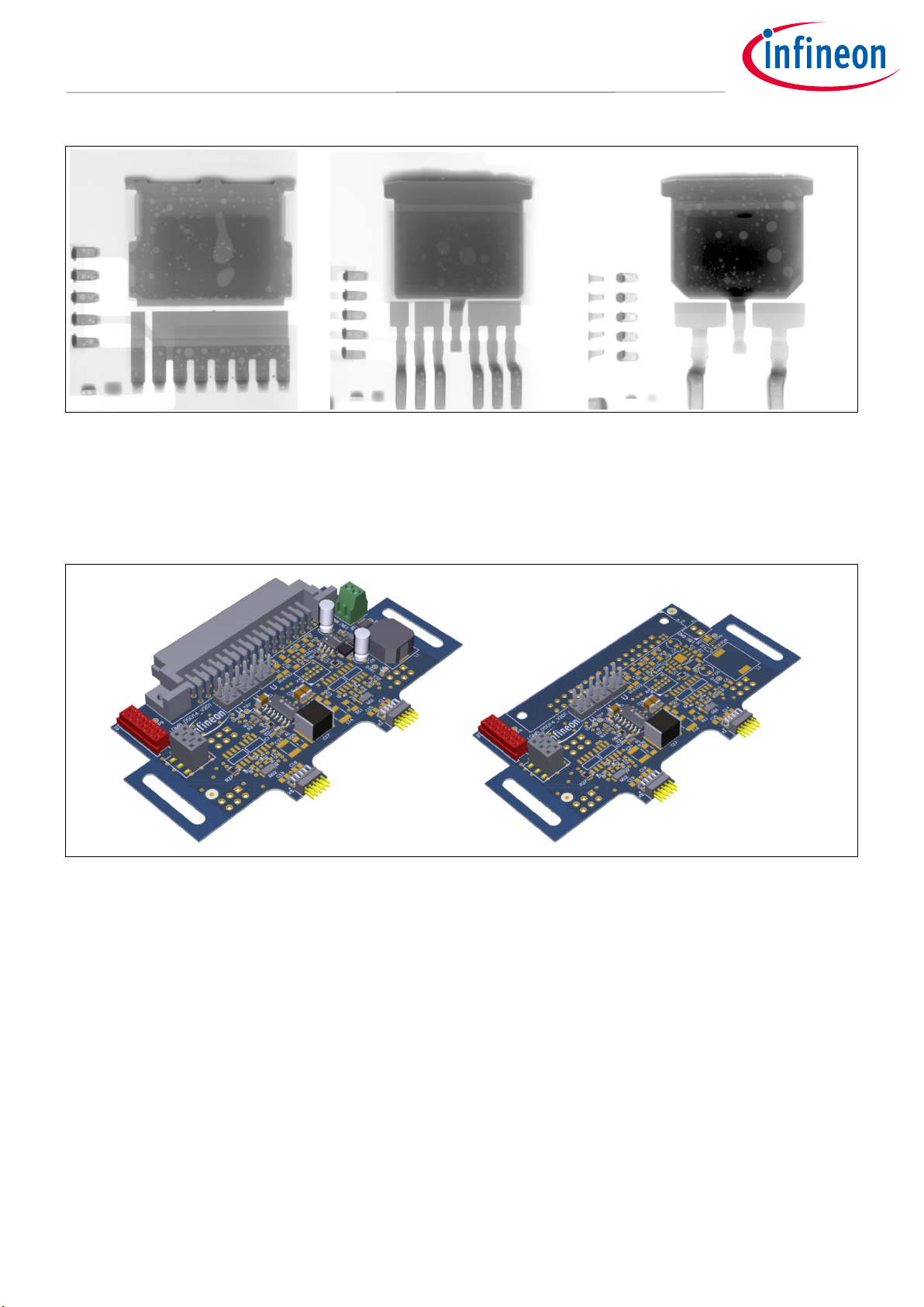
2.5 Control board
Various control boards can be adapted to interface the master mother board. The X3 connector (Hirose PCN1332S-2.54DS(71)) on the master mother board is provided for interfacing with Infineon’s XMC™ demonstration
board: XMC4400 drive card (KIT_XMC4400_DC_V1), which is used in the examples covered in this document.
The control signals are propagated to the master mother board gate driver, and the mother board bus as
described in chapter 3.2.
Figure 28 XMC4400 drive card demonstration board
A detailed description of the XMC4400 drive card can be found online.
Page 25

Application Note 25 of 54 V 1.1
2021-02-01
Scalable power inverter driving an electric motor
Using the low voltage drives scalable power demonstration board
Three-phase motor drive setup (B6)
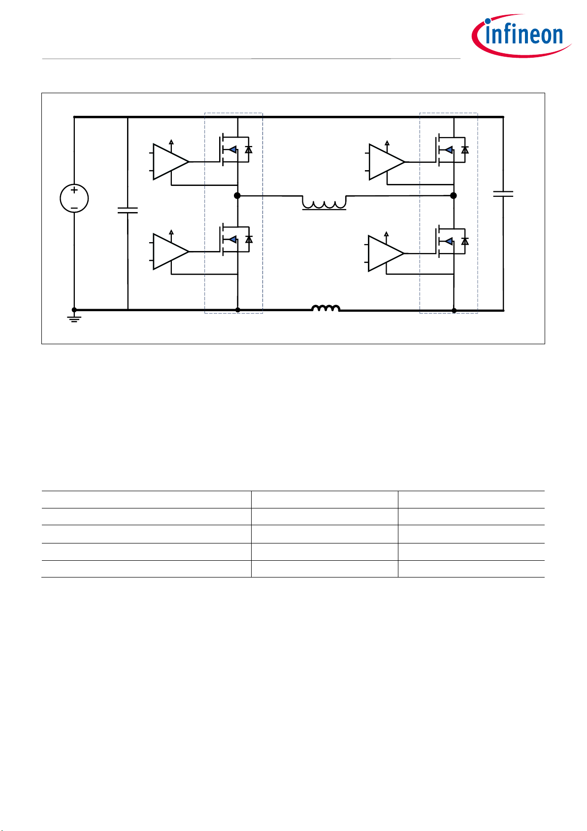
3 Three-phase motor drive setup (B6)
Alongside versatility, the platform was designed with motor drive applications in mind. The main focus of this
application note is therefore a three-phase motor drive setup (i.e. B6 inverter), represented in Figure 29. Some
performance examples of a B6 motor drive inverter, at different power board paralleling options, are given in
chapter 4.
Figure 29 B6 inverter – block diagram
Assembly procedures for constructing a B6 inverter can be found in the Low voltage drives scalable power
demo board – user manual.
Page 26

Application Note 26 of 54 V 1.1
2021-02-01
Scalable power inverter driving an electric motor
Using the low voltage drives scalable power demonstration board
Three-phase motor drive setup (B6)
3.1 Supply voltage
3.1.1 LV supply
The 15 V supply for the system connected at the X1 terminal is limited by the gate driver specification.
Table 6 LV system supply
Parameter
Values
Unit
Note
Min.
Typ.
Max.
LV system supply
12
15
20 V Max. according to 2EDL23N06PJ
3.1.2 Highvoltage/high power supply
Attention: In addition to high power supply voltage, the voltage spikes caused by MOSFET switching
need to be considered. The V
DSS
should not exceed the V
(BR)DSS
rating of the MOSFET at any
point. The supply voltage needs to be adapted accordingly.
The supply voltage used on the power side of the set-up will be limited by the MOSFET drain-source breakdown
voltage (V
(BR)DSS
). Recommended nominal supply voltages are given in Table 7, with regard to the breakdown
voltage rating of the MOSFET being used.
Table 7 Nominal power supply voltage recommendations
MOSFET V
(BR)DSS
rating (V)
Supply voltage
Unit
Typ.
Max.
60
24
32
V
80
48
V
100
48
V
150
72
96
V
200
144
V
250
157
V
3.2 Board interconnections in multiphase setups and power board
paralleling
Mother boards are used alongside a master mother board when two- or three-phase systems are implemented.
The mother boards are connected to the master mother board through the mother board bus via a ribbon cable
to connector X6, and provide the additional gate drivers for the additional two phases.
Daughter boards are used to propagate the gate driver signals to the power MOSFETs when paralleling of
power boards is implemented.
The following chapters describe the signals used to interconnect the boards in a particular setup.
Page 27

Application Note 27 of 54 V 1.1
2021-02-01
Scalable power inverter driving an electric motor
Using the low voltage drives scalable power demonstration board
Three-phase motor drive setup (B6)
3.2.1 Control signals – control board interface
The master mother board interface to the control board uses the pin-out as defined in the “Power board
connector” chapter of the XMC4400 drive card user manual: “Board_Users_Manual_DriveCard_XMC4400” found
on the demonstration board website:
https://www.infineon.com/cms/en/product/evaluation-boards/kit_xmc4400_dc_v1/
The document provides further details about the XMC4400 drive card.
The control board signals used are listed in Table 8 and Figure 30.
Table 8 Signal description
Signal name
Description
Comment
+5 V
XMCTM/control board supply
I_U, I_V, I_W
Current sensor feedback. From master
mother board onboard voltage
dividers/filters.
Optional – the voltage divider/filter
components are not populated by default
V_DClink
Supply voltage feedback. From master
mother board onboard voltage
divider/filter.
Optional – the voltage divider/filter
components are not populated by default
U_L, U_H, V_L,
V_H, W_L, W_H,
Gate driver control signals
CTRAP0, CTRAP1
Digital feedback signals connected to the
µC pins with “TRAP Function” capability
See XMC4400 microcontroller reference
manual for details
ENPOW0
Gate driver enable signal
Figure 30 XMC
TM
drive card connector pin-out – mother board PCB top view
Page 28

Application Note 28 of 54 V 1.1
2021-02-01
Scalable power inverter driving an electric motor
Using the low voltage drives scalable power demonstration board
Three-phase motor drive setup (B6)
3.2.2 Mother board bus
The mother board bus (ribbon cable connected at connector X6) propagates the gate drive control signals to
the “W” and “V” mother boards. It also connects the gate driver supply (15 V), and the gate driver enable signal.
ENPOW0 can be used to disable the gate drivers via the microcontroller. CTRAP1 connects all the gate driver
enable pins to a common pull-up to enable them. A fault condition (disable) on the gate driver will pull its
enable pin down (open drain configuration). This pull-down will also be propagated across CTRAP1 to the other
gate drivers, to disable them.
Figure 31 Mother board bus pin-out – top view
Selection jumpers “U”, “V” and “W” are provided to assign the control signals to each of the gate drivers. Since
all three control signals are present on the master mother board, and “V” and “W” control signals are present at
the mother board bus (propagated through the ribbon cable), the jumpers are used to physically connect either
of them to the gate driver inputs. In a three-phase setup the master mother board shall always be selected as
the “U” phase, since the “U” control signals are not present at the mother board bus.
Phase “U” Phase “V” Phase “W”
Figure 32 Jumper placement for phase selection
Page 29

Application Note 29 of 54 V 1.1
2021-02-01
Scalable power inverter driving an electric motor
Using the low voltage drives scalable power demonstration board
Three-phase motor drive setup (B6)
3.2.3 Daughter board bus
In the case of power board paralleling, the gate driver output signals are propagated to the parallel power
MOSFETs via X7 or X11 headers that branch out the gate driver output and source connections through the
corresponding daughter boards. The pin-out is shown in Figure 33.
All the nodes (gate driver outputs) are therefore present on all the daughter boards. The gate driver outputs
pass through a gate resistor at each of the daughter boards and connect to the power board (gate terminal).
Figure 33 Daughter board bus pin-out – top view
3.3 Using the V/f control for induction motor
Infineon provides a software package supporting the demonstration board. The software package is intended
for use with the B6 set-up to drive a three-phase induction motor. Provided in the software package are the
firmware for Infineon’s XMC™ demonstration board XMC4400 drive card, and a GUI for controlling the set-up.
The implemented induction motor drive firmware is based on the open-loop V/f control scheme. In principle V/f
control uses voltage sine wave signals to drive the motor. It varies the voltage signal amplitude in linear
relation to field rotation speed (electrical frequency of the motor). In switch-mode applications (utilizing the B6
topology) the voltage sine waves are generated via PWM signals at each of the phases, resulting in effective
voltages equivalent to the sine wave signals that the V/f ratio refers to.
The implemented characteristics of voltage amplitude in relation to the motor electrical frequency are shown
in Figure 34.
Ideally the ratio is maintained all the way to zero; however, at low speeds the voltage is typically increased to
compensate for the voltage drop across the stator resistance, which is not negligible at small voltages. This
voltage increase for low speeds is determined by the “V offset”, also seen in Figure 34.
Page 30

Application Note 30 of 54 V 1.1
2021-02-01
Scalable power inverter driving an electric motor
Using the low voltage drives scalable power demonstration board
Three-phase motor drive setup (B6)
Figure 34 V/f control characteristics with V offset implementation
The V/f ratio, V offset and field rotation speed (i.e. synchronous speed) are adjustable by the user via GUI
parameters. The first and second tab of the GUI are shown in Figure 35 and Figure 36.
Figure 35 GUI – motor control tab
Page 31

Application Note 31 of 54 V 1.1
2021-02-01
Scalable power inverter driving an electric motor
Using the low voltage drives scalable power demonstration board
Three-phase motor drive setup (B6)
The V/f ratio is set by the user according to motor characteristics and the applied load. For a given motor at
stable supply voltage, the load will determine the maximum achievable turning speed according to torque vs.
phase voltage characteristics of the motor.
The DC bus utilization bar represents roughly the ratio between the effective phase voltage amplitude and
supply voltage. It indicates the maximum duty cycle of the PWM within the motor electrical period.
In effect, the bar indicates the limit of the motor control settings – it considers the following parameters:
Input voltage (V)
Field rotation speed (RPM)
Voltage/frequency ratio (mV/Hz)
V/f offset
The limit is set to 90 percent, which also takes into consideration minimum charge times for charging a HS
bootstrap capacitor (some margin also included). The bootstrap is charged when the LS MOSFET conducts. The
critical timings in this regard are therefore achieved during high PWM duty cycles.
Figure 36 GUI – settings tab
Page 32

Application Note 32 of 54 V 1.1
2021-02-01
Scalable power inverter driving an electric motor
Using the low voltage drives scalable power demonstration board
Three-phase motor drive setup (B6)
Table 9 lists the parameters used by the GUI for interfacing the microcontroller.
Table 9 GUI settings description
Setting
Description
Field rotation speed
(RPM)
Setting of the stator field rotation speed. Type the value and confirm with “ENTER”, or
use the mouse scroll button while hovering above the value.
Voltage/frequency
ratio (mV/Hz)
The ratio of effective output voltage amplitude vs. field rotation speed
Number of motor
poles
Counted in stator pole pairs
V/f offset (mV)
Effective output voltage at standstill – see Figure 34 for characteristic curve. Set to zero
for linear V/f charateristics.
Ramp up (Hz/s)
Rate of change of the field rotation speed (when changing field rotation speed setting)
Input voltage (V)
DC power supply voltage used
I sensor gain (mV/A)
Gain of the current sensor used in mV/A
(It is recommended to use sensors with galvanic isolation, e.g. the ASC758 (±200 A
range, 10 mV/A output gain)
Current limit (A)
Current limit – disable if not using a sensor
PWM frequency (Hz)
PWM frequency setting
Dead-time (ns)
Dead-time setting (off-time of the complementary control signals)
3.3.1 Using the GUI
While the microcontroller is running the V/f control algorithm, the user can control the motor via parameters
provided by the GUI.
Before any parameter can be set, the GUI needs to establish connections with the microcontroller. The
interface settings can be found on the XMC_Connection tab, in the upper left corner (Figure 36). Set the baud
rate to 115200, and after connecting the drive card to a USB port, refresh the ports and select the
corresponding port with the drop-down menu.
When the connection is established the GUI will run a short diagnostics procedure on communication with the
microcontroller, and update the parameters on the microcontroller according to the parameters set on the GUI.
If the diagnostics show an error in GUI performance, or a restart of the GUI, the parameters will be sent from the
microcontroller to the GUI.
3.3.2 Configuration parameters
Before turning on the motor, the configuration parameters on the XMC_Communication tab need to be set.
Different methods of changing the parameters are available. The six parameters marked by the orange boxin
Figure 37 have three options for setting the value:
Scrolling with the mouse wheel while hovering above the box (value change is three units per scroll step)
→ µC is updated continuously
Clicking the up/down arrows (value change is one unit per click)
→ µC is updated continuously
Typing the new value in the box and pressing “ENTER”
In this case a warning window will ask to “Confirm updating”
→ µC is updated after confirming by pressing “Yes” (pressing “No” recovers previous value)
Page 33

Application Note 33 of 54 V 1.1
2021-02-01
Scalable power inverter driving an electric motor
Using the low voltage drives scalable power demonstration board
Three-phase motor drive setup (B6)
Figure 37 GUI – configuration parameters
The other two parameters in Figure 37 – “Number of motor poles” and “Ramp up” are only set by entering the
required value and configuring by pressing “ENTER”. The microcontroller is updated immediately.
It is not possible to change the configuration parameters during motor operation. If attempted the GUI will
return a warning, turning the data cell red, and the parameter will not be updated in the microcontroller.
3.3.3 Motor control parameters
The motor control parameters located on the “Motor Control” tab of the GUI are intended to be set during
motor operation. Thay can be set in the same manner as the parameters in Figure 37. The small difference in
setting the “Field Rotation Speed” is that the arrow buttons change the value by 30 units in this case. Entering a
value by typing again requires confirmation in order to avoid accidental large steps.
After setting the synchronous speed and the V/f ratio, pressing the “Start” button will begin to ramp up the
speed with the rate defined by the “Ramp up” configuration parameter. The button changes to “Stop”. Pressing
“Stop” will ramp the speed down at the same rate as the ramp up.
Attention: Stopping the motor with the “Stop” button does not disable the PWM. There is a small PWM
output present even at standstill. This is the “V offset” that is set in the configuration
parameters tab.
Located on both tabs of the GUI is the “Emergency stop” button. Pressing this, unlike pressing stop, will
immediately disable the gate drivers, thus turning off all of the power MOSFETs. The GUI will change the field
rotation speed to zero, and notify the user that the controller has entered “Emergency stop state”. To return
the controller to normal operation, the user needs to re-enable the system by pressing the “Enable_Inverter”
button on the “XMC_Connection” tab.
Page 34

Application Note 34 of 54 V 1.1
2021-02-01
Scalable power inverter driving an electric motor
Using the low voltage drives scalable power demonstration board
Three-phase motor drive setup (B6)
Figure 38 Re-enable inverter after emergency stop
Attention: Make sure to check any potential failures that might have been the cause for the emergency
stop, before re-enabling the inverter!
3.3.4 Driving an induction motor
Depending on the type of load used, the approach of utilizing the V/f method can vary.
On a typical laboratory test bench, using an adjustable load, it is common to change the load at a constant
synchronous speed. Changing the load requires changing the voltage amplitude, so that the slip is maintained
at the rated value. If the slip is increased beyond the point of maximum motor torque, the motor will stall,
causing a considerable increase in phase currents. Using current limitation on the power supply is
recommended.
At a constant setting of the field rotation speed parameter in the GUI, the V/f ratio setting in effect only changes
the voltage amplitude. An easy way to establish an operating point for measurements is to start the motor with
a relatively small V/f ratio setting while keeping the load disabled. After settling at the target speed (rotor slip
considered), the load can be increased simultaneously or alternating with the voltage amplitude.
The actual V/f value required to start turning the motor will depend on the motor characteristics, the load
(including friction losses) and the rotor inertia (including inertia of the brake and any additional mass
attached). Since the inertia will affect torque applied to the motor during acceleration, the ramp-up rate will
also have an effect.
Insufficient values of V/f will result in considerable rotor delays at start-up, or not starting at all. If the response
is considerable at the beginning of ramp-up, but catches up with the field rotation speed before the end of the
ramp up process, it can be speeded up by increasing the V offset in order to increase the tourqe at low
frequencies.
Page 35

Application Note 35 of 54 V 1.1
2021-02-01
Scalable power inverter driving an electric motor
Using the low voltage drives scalable power demonstration board
Three-phase motor drive setup (B6)
When setting the paramenters, the user should consider that the synchronous speed is increased linearly after
pressing the “Start” button, and with proper settings the rotor should ramp-up linearly as well, with the
additional delay of the absolute slip speed (n
slip
= n
sync
– n
rotor
), which should ideally be kept constant.
A good way of evaluating the ramp-up procedure is also to observe the amplitudes of the phase currents during
ramp-up. The current amplitude is expected to be higher but constant during ramp-up, and to drop to a smaller
steady-state value when the rotor speed is settled.
V offset will keep a constant current flowing through the stator windings even at standstill, which can heat the
motor windings.
Excessive values of the V/f coefficient will increase the reactive current to the motor, resulting in higher losses,
and in extreme cases saturation of the stator.
Attention: Make sure that motor limits are not exceeded, or permanent damage to the motor and/or
inverter could occur.
Attention: There are exposed surface areas under high voltage in this setup. Make sure to secure the
setup against accidental contact by people or equipment.
Page 36

Application Note 36 of 54 V 1.1
2021-02-01
Scalable power inverter driving an electric motor
Using the low voltage drives scalable power demonstration board
Performance of a B6 setup in a motor drive application
4 Performance of a B6 setup in a motor drive application
Performance of a B6 inverter setup with a different number of paralleled power boards has been tested at
different operating points, to evaluate the capabilities of the setup. The power boards were cooled with
aluminum air-cooled heatsinks (each phase separately). The test setup was constructed using the
KIT_LGPWR_BOM003 power board version, which utilizes the IPT012N08N5 MOSFET with a V
(BR)DSS
rating of 80 V.
The B6 setup was used to drive an induction motor, with an electric brake providing the load.
The V/f control was used as described above.
Table 10 lists the components used in the performance tests.
Table 10 Setup overview for four paralleled power boards
Part
Description
Quantity
Power board
KIT_LGPWR_BOM003
12 pieces
Capacitor board
KIT_LGCAP_BOM005
3
Control board
KIT_XMC4400_DC_V1
1
Master mother board
KIT_LGMB_BOM003
1
Mother board
KIT_LGMB_BOM503
2
Daughter board
KIT_LGDB_BOM003
9
Heatsink (aluminum, air-cooled)
100 mm x 100 mm x 40 mm (fins: 30
mm)
3
Copper bars set
See user manual [1]
1 set
Copper spacer
See user manual [1]
6
Screw for power terminals
M5, 6 mm
48
Interconnection bolts and nuts
M5
11 sets
Screw for attaching IMS boards to heatsink
M2, 5 mm
72
Current sensor
VAC – P4640-X150
4
The operating points of the tests are differentiated by load/power output, while the conditions listed in Table
11 are the same for all cases.
Table 11 Specifications and conditions
Parameter
Value
Unit
Ambient temparature
23
°C
Power board break-down voltage
80
V
Supply voltage
48 V f_PWM
8
kHz
Dead-time
2
µs
R
G
47
Ω
Field rotation speed
1800
RPM
Mechanical speed
1760
RPM
Electrical frequency (field
frequency)
60
Hz
Page 37

Application Note 37 of 54 V 1.1
2021-02-01
Scalable power inverter driving an electric motor
Using the low voltage drives scalable power demonstration board
Performance of a B6 setup in a motor drive application
Using the GUI provided, the operating point was set by gradually increasing the mechanical load and the V/f
coefficient, at a constant synchronous speed.
The thermal images below show a single phase of the setup. The images are taken 3 minutes after reaching the
operating point, which is not fully settled at the heatsink temperature; however, the temperature of
components on the FR4 boards can be considered settled. As the following results show, the ceramic capacitors
on mother boards and daughter boards are often the limiting factor.
Table 12 lists an overview of the results.
Table 12 Overview of test operating point results
Parameter
OP1
OP2
OP3
OP4
OP5
Setup (parallel
MOSFETs per switch)
1 (no
paralleling)
1 (no
paralleling)
2 2 4
P supply [W]
2014.1
5233.1
5474.1
8860.2
10407.2
P electric out [W]
1814.5
4786.2
5112.7
8263.3
9595.7
Inverter efficiency [%]
90.1
91.5
93.4
93.3
92.2
Braking torque [Nm]
8.157
22.12
23.86
38.17
44.06
P mechanical [W]
1503
4078
4397
7034
8121
OP2 and OP4 can serve as good representatives of the setup capabilities. The power output of OP5 was not
limited by heat dissipation on the inverter. The operating point was set at maximum duty cycle of the PWM
signals. This means that the motor and load were defining the maximum load on the inverter in this operating
point. Depending on the load, the inverter with four parallel MOSFETs per switch will therefore be able to
handle even higher power.
4.1 No paralleling
The first two operating points were measured without using any paralleling of the power MOSFETs in the B6
inverter. The B6 setup therefore uses a single power board per phase. This is illustrated in Figure 39.
Page 38

Application Note 38 of 54 V 1.1
2021-02-01
Scalable power inverter driving an electric motor
Using the low voltage drives scalable power demonstration board
Performance of a B6 setup in a motor drive application
Figure 39 System block diagram – no MOSFET paralleling
4.1.1 Operating point 1
The measurement results of the first operating point are shown in Table 13.
Table 13 OP1 measurements
Parameter
Value
Unit
Torque
8.157
Nm
V/f setting
285
mV/Hz
P supply
2014.1
W
P electric
1814.5
W
Inverter efficiency
90.1
%
P mech
1503
W
Figure 40 shows the current waveforms – three-phase currents and supply current.
Page 39

Application Note 39 of 54 V 1.1
2021-02-01
Scalable power inverter driving an electric motor
Using the low voltage drives scalable power demonstration board
Performance of a B6 setup in a motor drive application
The relatively high current ripple at 8 kHz, due to the low inductance of the motor windings being used, is not
unusual; however, will cause additional losses on the motor.
When driving an induction motor, the control over the reactive component of phase currents is limited. The
reactive current is the reason for the relatively high amplitudes of the phase currents. This behavior can also be
observed in the other operating points.
Figure 40 Current waveforms
Ch1 (light blue): “U” phase current
Ch2 (yellow): “V” phase current
Ch3 (red): “W” phase current
Ch4 (dark blue): DC supply current
Figure 41 shows the thermal distribution after 3 minutes. According to component temperatures, the system is
capable of handling higher loads.
Page 40

Application Note 40 of 54 V 1.1
2021-02-01
Scalable power inverter driving an electric motor
Using the low voltage drives scalable power demonstration board
Performance of a B6 setup in a motor drive application
Figure 41 Top-side view and thermal distribution
Table 14 Temperature measurements from Figure 41
Measuring subject
Measuring point
Temperature [°C]
MOSFET_HS1
Area01 (max.)
67.7
MOSFET_LS1
Area02 (max.)
74.0
Heatsink
Spot01
57.0
Spot02
57.7
Average
55.8
4.1.2 Operating point 2
This operating point was tuned to represent the maximum achievable power output of the non-paralleled
system, without exceeding a temperature of 120°C. The results are shown in Table 15.
The current waveforms are shown in Figure 42.
Table 15 OP2 measurements
Parameter
Value
Unit
Torque
22.12
Nm
V/f setting
467
mV/Hz
P supply
5233.1
W
P electric
4786.2
W
Inverter efficiency
91.5
%
P mech
4078
W
Page 41

Application Note 41 of 54 V 1.1
2021-02-01
Scalable power inverter driving an electric motor
Using the low voltage drives scalable power demonstration board
Performance of a B6 setup in a motor drive application
Figure 42 Current waveforms
Ch1 (light blue): “U” phase current
Ch2 (yellow): “V” phase current
Ch3 (red): “W” phase current
Ch4 (dark blue): DC supply current
Figure 43 shows the thermal distribution after 3 minutes of operation in this operating point. The temperature
difference between the hottest MOSFET and the heatsink in its proximity is ∆T
LS1
= 48.1 K.
Page 42

Application Note 42 of 54 V 1.1
2021-02-01
Scalable power inverter driving an electric motor
Using the low voltage drives scalable power demonstration board
Performance of a B6 setup in a motor drive application
Figure 43 Top-side view and thermal distribution
Table 16 Temperature measurements from Figure 43
Measuring subject
Measuring point
Temperature [°C]
MOSFET_HS1
Area01 (max.)
97.7
MOSFET_LS1
Area02 (max.)
114.7
Heatsink
Spot01
65.4
Spot02
66.6
Average
61.8
4.2 Two-per-phase parallel connection
The setup used for the following two operating points is illustrated in Figure 44. It uses two power boards
connected in parallel for each phase. It uses an additional daughter board in each phase to connect the
paralleled power boards to the gate drivers.
Page 43

Application Note 43 of 54 V 1.1
2021-02-01
Scalable power inverter driving an electric motor
Using the low voltage drives scalable power demonstration board
Performance of a B6 setup in a motor drive application
Figure 44 System block diagram – two parallel power boards per phase
4.2.1 Operating point 3
This operating point was selected to use the same V/f setting as OP2, meaning that the PWM signals are the
same. In an ideal setup this would exactly recreate the operating point; however, due to paralleling, the system
performs differently. The results are shown in Table 17.
Table 17 OP3 measurements
Parameter
Values
Unit
Torque
23.86
Nm
V/f setting
467
mV/Hz
P supply
5474.1
W
P electric
5112.7
W
Inverter efficiency
93.4
%
P mech
4397
W
Page 44

Application Note 44 of 54 V 1.1
2021-02-01
Scalable power inverter driving an electric motor
Using the low voltage drives scalable power demonstration board
Performance of a B6 setup in a motor drive application
Figure 45 shows the current waveforms.
Figure 45 Current waveforms
Ch1 (light blue): “U” phase current
Ch2 (yellow): “V” phase current
Ch3 (red): “W” phase current
Ch4 (dark blue): DC supply current
Figure 46 shows the thermal distribution after 3 minutes of operation. Compared to OP2, there is a
considerable reduction of MOSFET temperatures as expected; however, there is an increase in heat dissipation
on the ceramic DC capacitors on FR4 boards. Since these components are not cooled via IMS boards as the
MOSFETs, the capacitors can reach similar temperatures as the MOSFETs at considerably lower power
dissipation. However, there is an increase in capacitor temperatures in comparison with the non-paralelled
setup. In addition to providing most of the charge during the half-bridge switching transitions, there are
additional losses caused by oscillations between the paralleled capacitors, after each switching transition. The
oscillations are attributed to the unavoidable parasitic inductances surrounding the ceramic capacitors that
are integrated into the system due to the manner of interconnecting the modular half-bridges. The capacitors
and the parasitic inductances therefore form localized C-L resonant subcircuits that add to the current
oscillation of each capacitor, immediately after MOSFET turn-on.
Page 45

Application Note 45 of 54 V 1.1
2021-02-01
Scalable power inverter driving an electric motor
Using the low voltage drives scalable power demonstration board
Performance of a B6 setup in a motor drive application
Figure 46 Top-side view and thermal distribution
Table 18 Temperature measurements from Figure 46
Measuring subject
Measuring point
Temperature [°C]
C
DC_2
Area01 (max.)
74.3
MOSFET_HS2
Area02 (max.)
60.9
MOSFET_LS2
Area03 (max.)
60.2
MOSFET_HS1
Area04 (max.)
64.2
MOSFET_LS1
Area05 (max.)
66.1
Heatsink
Spot01
50.8
Spot02
51.1
Average
49.4
Page 46

Application Note 46 of 54 V 1.1
2021-02-01
Scalable power inverter driving an electric motor
Using the low voltage drives scalable power demonstration board
Performance of a B6 setup in a motor drive application
4.2.2 Operating point 4
This operating point represents the maximum achievable power output of the setup with two paralleled power
boards per phase. On top of keeping the temperatures of MOSFETs within safe limits, the ceramic capacitor
temperatures are not to exceed 110°C (some safety margin considered). The results are shown in Table 19.
Table 19 OP4 measurements
Parameter
Value
Unit
Torque
38.17
Nm
V/f setting
617
mV/Hz
P supply
8860.2
W
P electric
8263.3
W
Inverter efficiency
93.3
%
P mech
7034
W
Figure 47 shows the current waveforms.
Figure 47 Current waveforms
Page 47

Application Note 47 of 54 V 1.1
2021-02-01
Scalable power inverter driving an electric motor
Using the low voltage drives scalable power demonstration board
Performance of a B6 setup in a motor drive application
Ch1 (light blue): “U” phase current
Ch2 (yellow): “V” phase current
Ch3 (red): “W” phase current
Ch4 (dark blue): DC supply current
Figure 48 shows the thermal distribution after 3 minutes of operation. As explained in the previous subchapter,
the ceramic capacitors connected to the DC bus, are the hottest components and will therefore represent the
limiting factor of the setup.
A way to reduce the losses on the ceramics capacitors by reducing the oscillating current ripples would be to
reduce the value of the capacitance of the ceramic capacitors. However, when doing so, an increase of the
voltage overshoot during switching is to be expected. Further tuning the setup according to requirements will
therefore incude a trade-off between the two.
Figure 48 Top-side view and thermal distribution
Table 20 Temperature measurements from Figure 48
Measuring subject
Measuring point
Temperature [°C]
C
DC_2
Area01 (max.)
106.9
MOSFET_HS2
Area02 (max.)
87.5
MOSFET_LS2
Area03 (max.)
84.8
MOSFET_HS1
Area04 (max.)
92.8
MOSFET_LS1
Area05 (max.)
94.3
Heatsink
Spot01
68.6
Spot02
69.9
Average
66.2
Page 48

Application Note 48 of 54 V 1.1
2021-02-01
Scalable power inverter driving an electric motor
Using the low voltage drives scalable power demonstration board
Performance of a B6 setup in a motor drive application
4.3 Four-per-phase parallel connection
The setup uses four power boards connected in parallel for each phase, as is illustrated in Figure 51. Three
daughter boards are added to each phase to connect the paralleled power boards to the corresponding gate
drivers.
Figure 49 System block diagram – four parallel power boards per phase
Page 49

Application Note 49 of 54 V 1.1
2021-02-01
Scalable power inverter driving an electric motor
Using the low voltage drives scalable power demonstration board
Performance of a B6 setup in a motor drive application
4.3.1 Operating point 5
In this operating point, besides the ceramic capacitor thermal limit, the load also represents a limiting factor.
The V/f setting has been set to the point of maximum allowed PWM duty cycle. The results are shown in Table
21.
Table 21 OP5 measurements
Parameter
Value
Unit
Torque
44.06
Nm
V/f setting
671
mV/Hz
P supply
10407.2
W
P electric
9595.7
W
Inverter efficiency
92.2
%
P mech
8121
W
The waveforms are shown in Figure 50.
Figure 50 Current waveforms
Page 50

Application Note 50 of 54 V 1.1
2021-02-01
Scalable power inverter driving an electric motor
Using the low voltage drives scalable power demonstration board
Performance of a B6 setup in a motor drive application
Ch1 (light blue): “U” phase current
Ch2 (yellow): “V” phase current
Ch3 (red): “W” phase current
Ch4 (dark blue): DC supply current
Figure 51 shows the thermal distribution after 3 minutes of operation. The effect of the current oscillations on
the ceramic capacitors is even more pronounced with expanded paralleling. As mentioned in chapter 4.2.1,
reducing the ceramic capacitance values needs to be handled in accordance with switching performance.
Figure 51 Top-side view and thermal distribution
Table 22 Temperature measurements from Figure 51
Measuring subject
Measuring point
Temperature [°C]
C
DC_2
Area01 (max.)
109.0
MOSFET_HS4
Area02 (max.)
86.3
MOSFET_LS4
Area07 (max.)
83.8
MOSFET_HS3
Area03 (max.)
89.6
MOSFET_LS3
Area06 (max.)
87.0
MOSFET_HS2
Area04 (max.)
88.9
MOSFET_LS2
Area08 (max.)
87.2
MOSFET_HS1
Area05 (max.)
92.5
MOSFET_LS1
Area09 (max.)
90.9
Heatsink
Spot01
79.8
Spot02
79.7
Average
79.4
Page 51

Application Note 51 of 54 V 1.1
2021-02-01
Scalable power inverter driving an electric motor
Using the low voltage drives scalable power demonstration board
Summary
5 Summary
The modular demonstration board represesnts a versatile platform that provides the means to construct a
functional setup, intended for laboratory test bench work, product evaluation and switching performance
trimming. This document provides the necessary information about the modules to enable the user to
implement and adapt the boards to specific project requirements. It should be considered that the modular
nature of the platform and adaptation to measurement equipment accessibility require some trade-offs in the
design with regard to performance. This means that any setup built based on the platform can be improved by
optimizing the layout in further design processes. An easy approach, ensuring noticeable improvements, is to
stack the capacitor bank as well as the control circuitry on top of the power boards. However, these kinds of
setups become harder to probe with measurement equipment.
Even though the platform was optimized for measurement purposes, the main effects on performance can still
be observed and influenced on a proof-of-concept setup constructed using the low voltage drives scalable
power demonstration board platform.
Page 52

Application Note 52 of 54 V 1.1
2021-02-01
Scalable power inverter driving an electric motor
Using the low voltage drives scalable power demonstration board
References
6 References
[1] Infineon user manual UM_1901_PL51_1903_145150: Low voltage drives scalable power demonstration
board, User_manual_Low voltage drives scalable power demoboard (infineon.com)
[2] Infineon application note: Recommendations for assembly of Infineon TO packages
[3] EiceDRIVER™ 1EDN-TDI low-side gate drivers, Infineon Technologies, 2019,
https://www.infineon.com/1edn-tdi
[4] Infineon application note AN_1803_PL52_1804_112257: Applications of 1EDNx550 single-channel low-
side EiceDRIVER™ with truly differential inputs, https://www.infineon.com/dgdl/Infineon-
EiceDRIVER_1EDN_TDI_1EDNx550-ApplicationNotes-v03_00EN.pdf?fileId=5546d462636cc8fb016387e66c73160f
Page 53

Application Note 53 of 54 V 1.1
2021-02-01
Scalable power inverter driving an electric motor
Using the low voltage drives scalable power demonstration board
Revision history
Revision history
Document
version
Date of release
Description of changes
V 1.0
23-09-2019
First release
V 1.1
01-02-2021
Gate drivers option II chapter added
Page 54

Trademarks
All referenced product or service names and trademarks are the property of their respective owners.
Edition 2021-02-01
AN_1906_PL18_1908_180413
Published by
Infineon Technologies AG
81726 Munich, Germany
© 2021 Infineon Technologies AG.
All Rights Reserved.
Do you have a question about this
document?
Email: erratum@infineon.com
Document reference
IMPORTANT NOTICE
The information contained in this application note
is given as a hint for the implementation of the
product only and shall in no event be regarded as a
description or warranty of a certain functionality,
condition or quality of the product. Before
implementation of the product, the recipient of this
application note must verify any function and other
technical information given herein in the real
application. Infineon Technologies hereby
disclaims any and all warranties and liabilities of
any kind (including without limitation warranties of
non-infringement of intellectual property rights of
any third party) with respect to any and all
information given in this application note.
The data contained in this document is exclusively
intended for technically trained staff. It is the
responsibility of customer’s technical departments
to evaluate the suitability of the product for the
intended application and the completeness of the
product information given in this document with
respect to such application.
For further information on the product, technology,
delivery terms and conditions and prices please
contact your nearest Infineon Technologies office
(www.infineon.com).
WARNINGS
Due to technical requirements products may
contain dangerous substances. For information on
the types in question please contact your nearest
Infineon Technologies office.
Except as otherwise explicitly approved by Infineon
Technologies in a written document signed by
authorized representatives of Infineon
Technologies, Infineon Technologies’ products may
not be used in any applications where a failure of
the product or any consequences of the use thereof
can reasonably be expected to result in personal
injury.
 Loading...