

j
g
查询SMBD914供应商
Silicon Switching Diode
• For high-speed switching applications
SMBD914/MMBD914
SMBD914/MMBD914...
3
1 2
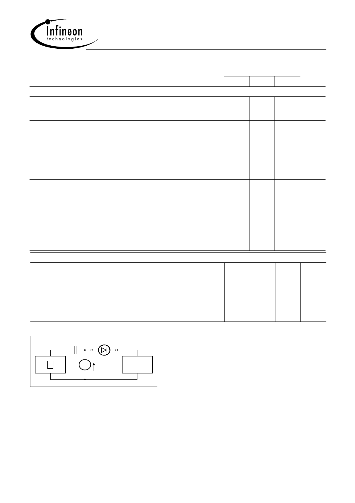
Type Package Configuration Marking
SMBD914/MMBD914 SOT23 single s5D
Maximum Ratings at TA = 25°C, unless otherwise specified
Parameter Symbol Value Unit
Diode reverse voltage V
Peak reverse voltage V
Forward current I
Non-repetitive peak surge forward current
t = 1 µs
t = 1 s
Total power dissipation
T
≤ 54°C
S
Junction temperature T
F
I
FSM
P
R
RM
tot
100 V
100
250 mA
A
4.5
0.5
370 mW
150 °C
Storage temperature T
st
-65 ... 150
Thermal Resistance
Parameter Symbol Value Unit
Junction - soldering point1)
R
thJS
≤ 260
K/W
SMBD914/MMBD914
1
For calculation of R
please refer to Application Note Thermal Resistance
thJA
1
Mar-10-2004
SMBD914/MMBD914...
Electrical Characteristics at TA = 25°C, unless otherwise specified
Parameter
DC Characteristics
Breakdown voltage
= 100 µA
I
(BR)
Reverse current
= 20 V
V
R
V
= 75 V
R
V
= 20 V, TA = 150 °C
R
V
= 75 V, TA = 150 °C
R
Forward voltage
I
= 1 mA
F
= 10 mA
I
F
I
= 50 mA
F
I
= 100 mA
F
I
= 150 mA
F
Symbol Values Unit
min. typ. max.
V
I
V
R
(BR)
F
100 - - V
-
-
-
-
-
-
-
-
-
-
-
-
-
-
-
-
-
-
0.025
0.1
30
50
715
855
1000
1200
1250
µA
mV
AC Characteristics
Diode capacitance
V
= 0 V, f = 1 MHz
R
Reverse recovery time
I
= 10 mA, IR = 10 mA, measured at IR = 1mA ,
F
R
= 100 Ω
L
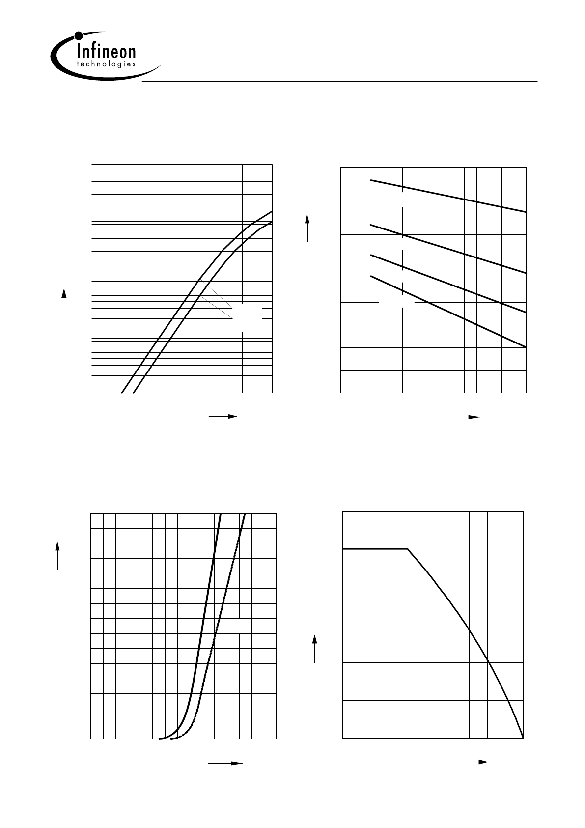
Test circuit for reverse recovery time
D.U.T.
Pulse generator: tp = 100ns, D = 0.05, tr = 0.6ns,
R
Ι
F
Oscillograph
Oscillograph: R = 50Ω, t
EHN00019
C
t
T
rr
- - 2 pF
- - 4 ns
= 50Ω
i
= 0.35ns, C ≤ 1pF
r
2
Mar-10-2004
SMBD914/MMBD914...
Reverse current I
V
= Parameter
R
5
10
nA
4
10
R
I
3
10
2
10
1
10
0 25 50 75 100
= ƒ (T
R
)
A
Forward Voltage V
I
= Parameter
F
SMBD 914 EHB00114
1.0
= ƒ (T
F
)
A
V
Ι
= 100 mA
V
F
F
10 mA
0.5
1 mA
0.1 mA
70 V
25 V
°C
150
T
A
0
0 50 100 150
˚C
T
A
Forward current I
T
= 25°C
A
150
Ι
F
mA
100
50
0
0
= ƒ (V
F
)
F
EHB00137SMBD 7000
maxtyp
0.5 1.0 V 1.5
V
F
Forward current I
= ƒ (T
F
SMBD914/MMBD914
300
mA
200
F
I
150
100
50
0
0 15 30 45 60 75 90 105 120
)
S
°C
150
T
S
3
Mar-10-2004
SMBD914/MMBD914...
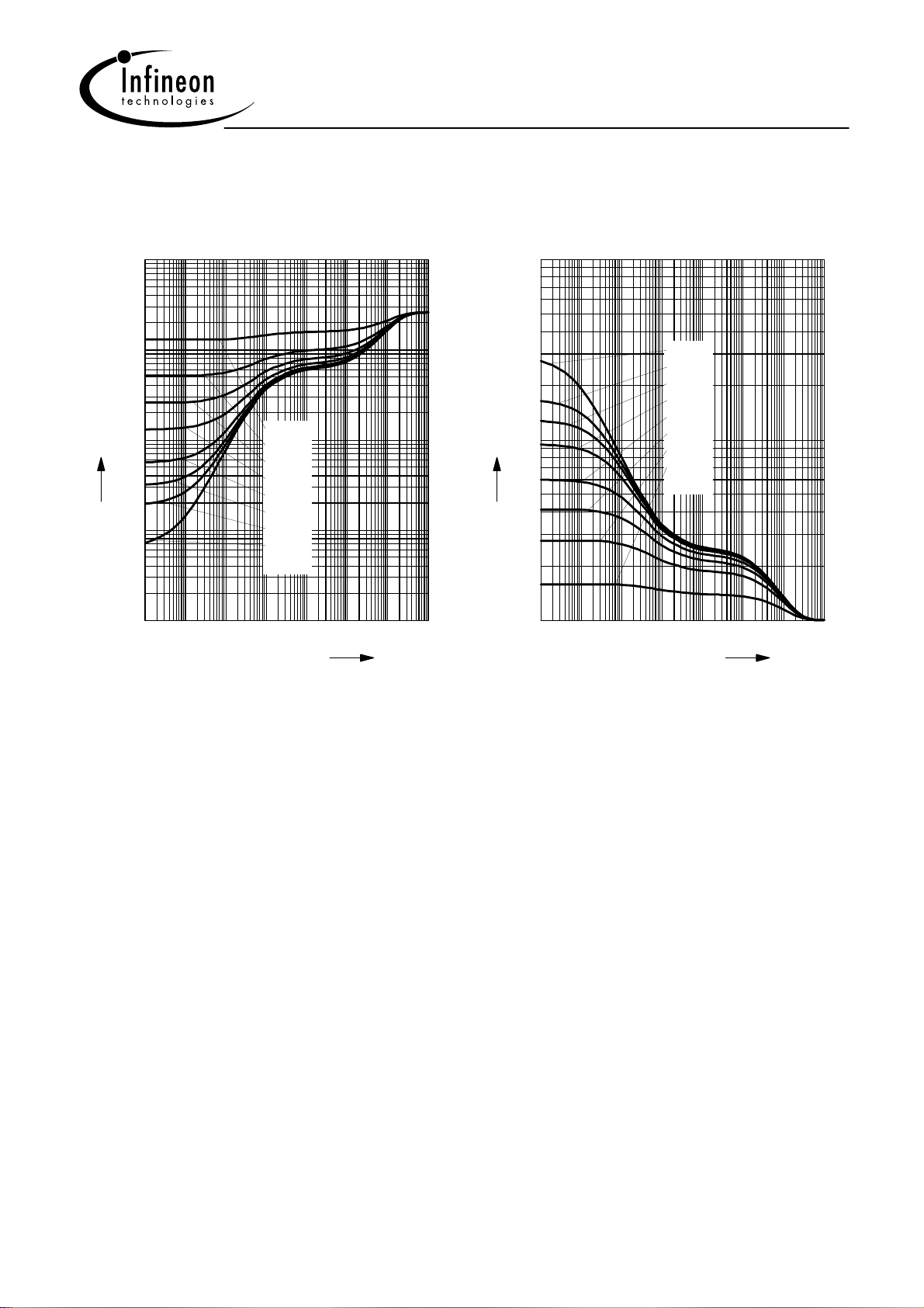
Permissible Puls Load R
3
10
K/W
2
10
thJS
R
10
10
10
1
0
-1
-7
10
-6
10
10
0.5
0.2
0.1
0.05
0.02
0.01
0.005
D = 0
-5
-4
10
thJS
10
= ƒ (t
-3
10
)
p
Permissible Pulse Load
I
Fmax
FDC
/I
Fmax
I
/ I
10
FDC
2
= ƒ (t
)
p
D = 0
0.005
0.01
0.02
0.05
10
1
0.1
0.2
0.5
0
-2
s
t
0
10
p
10
10
-7
-6
-5
-4
-3
10
10
10
10
10
-2
s
t
0
10
p
4
Mar-10-2004
 Loading...