

INFINEON MA5332MS Datasheet

MA5332MS
200W Stereo, Integrated Class D Amplifier
Features
2 channel analog input Class D audio amplifier in a small 7x7mm package
Very low R
95% efficiency Class D at 2x200W at 4Ω
Split or single power supply capable
Differential or single-ended input
Multiple configuration options: 2xSE, BTL, PSE (Parallel Single-Ended)
Over-current, over-temperature and under-voltage protections with self-reset feature
Start/stop click noise reduction
Clip and Fault reporting outputs
Applications
Multi-channel home theatre system
Studio monitor
Active speaker
Soundbar subwoofer
Marine amplifier
Aftermarket car audio system
General-purpose audio power amplifier
Product validation
at 24.4 mΩ typical, enabling heatsink-less operation at 2x100W at 4Ω
DS(ON)
Total Harmonic Distortion
PG- IQFN-42
Qualified for standard applications according to the
relevant tests of J-STD-020 and JESD22.
Product type Package
MA5332MS 7x7mm PG- IQFN-42
Description
The MA5332MS offers the same or higher output power than monolithic alternatives without heatsink and 50%
less footprint. This MCM (multi-chip module) solution integrates 2 channel PWM controller, high voltage gate
driver, and 4 low R
features for reliable operation over various environmental conditions. As a powerful upgrade to IR43x2M and
other monolithic solutions, MA5332MS’ 7x7 mm PG- IQFN-42 package showcases the benefit of small footprint,
high power density, and heatsink-less operation.
Topology Half-bridge / Full bridge
MA5332MS Output power (Halfbridge,THD+N=10%, typical)
*Residual noise (AES-17, IHF-A, typical) 250 μVrms
*THD+N (1kHz, 70W, 4 Ω, typical) 0.01 %
* In a typical application
MOSFETs. Like its predecessor, IR43x2M, it includes standard Class D protection
DS(ON)
150 W in 2 Ω / 300 W in 4 Ω
200 W in 4 Ω / 400 W in 8 Ω
160 W in 6 Ω
Datasheet Please read the Important Notice and Warnings at the end of this document V 2.0
www.infineon.com page 1 of 59 9/24/2021

MA
5332MS
Table of contents
Integrated Class D Amplifier
Table of contents
Features ........................................................................................................................................ 1
Applications ................................................................................................................................... 1
Product validation .......................................................................................................................... 1
Description .................................................................................................................................... 1
Table of contents ............................................................................................................................ 2
1 Qualification information ........................................................................................................ 4
2 Device Comparison Table ........................................................................................................ 5
3 Pin Configuration ................................................................................................................... 6
3.1 Lead assignments .................................................................................................................................... 6
3.2 Lead definitions ....................................................................................................................................... 7
4 Specifications ........................................................................................................................ 8
4.1 Absolute maximum ratings ..................................................................................................................... 8
4.2 Recommended operating conditions ..................................................................................................... 9
4.3 Electrical characteristics ....................................................................................................................... 10
4.4 Audio characteristics (SE) ..................................................................................................................... 13
4.5 Audio characteristics (BTL) ................................................................................................................... 13
4.6 Audio characteristics (PSE) ................................................................................................................... 14
4.7 Typical Audio characteristics (SE) ........................................................................................................ 15
4.7.1 Power vs. THD+N .............................................................................................................................. 15
4.7.2 Frequency vs. THD+N ....................................................................................................................... 16
4.7.3 Frequency response ......................................................................................................................... 16
4.7.4 Noise floor ........................................................................................................................................ 17
4.7.5 Efficiency .......................................................................................................................................... 17
4.8 Typical Audio characteristics (BTL) ...................................................................................................... 18
4.8.1 Power vs. THD+N .............................................................................................................................. 18
4.8.2 Frequency vs. THD+N ....................................................................................................................... 19
4.8.3 Frequency response ......................................................................................................................... 19
4.8.4 Noise floor ........................................................................................................................................ 20
4.9 Typical Audio characteristics (PSE) ...................................................................................................... 21
4.9.1 Power vs. THD+N .............................................................................................................................. 21
4.9.2 Frequency vs. THD+N ....................................................................................................................... 22
4.9.3 Frequency response ......................................................................................................................... 22
4.9.4 Noise floor ........................................................................................................................................ 23
5 Thermal information ............................................................................................................. 24
5.1 Peak power duration thermal information .......................................................................................... 24
5.2 Heatsink information ............................................................................................................................ 28
6 Functional block diagram ....................................................................................................... 29
7 Typical Implementation ......................................................................................................... 30
8 Input / Output pin equivalent circuit diagrams ......................................................................... 33
9 PWM Modulator Design .......................................................................................................... 34
9.1 Input Section ......................................................................................................................................... 34
9.2 Control Loop Design .............................................................................................................................. 35
9.3 PWM Frequency ..................................................................................................................................... 35
9.4 Clock Synchronization .......................................................................................................................... 36
9.5 Click Noise Elimination ......................................................................................................................... 37
Datasheet 2 of 59 V 2.0
9/24/2021

MA
5332MS
Table of contents
Integrated Class D Amplifier
9.6 Differential Input ................................................................................................................................... 38
10 Operational Mode.................................................................................................................. 39
10.1 Self-oscillation Start-up Condition ....................................................................................................... 39
11 Protections ........................................................................................................................... 40
11.1.1 Self-Reset Protection ....................................................................................................................... 41
11.1.2 Designing Ct...................................................................................................................................... 42
11.1.3 Shutdown Input ............................................................................................................................... 42
11.1.4 Latched Protection........................................................................................................................... 43
11.1.5 Interfacing with System Controller ................................................................................................. 43
11.2 Over Current Protection (OCP) ............................................................................................................. 44
11.3 Over Temperature Protection (OTP) .................................................................................................... 45
11.4 Under Voltage Protection (UVP) ........................................................................................................... 45
12 Status Output ....................................................................................................................... 46
12.1 Fault Output .......................................................................................................................................... 46
12.2 CLIP Output ........................................................................................................................................... 47
13 Power Supply Design ............................................................................................................. 48
13.1 Supplying VAA and VSS ......................................................................................................................... 48
13.2 Supplying VCC and VB ........................................................................................................................... 48
13.2.1 Choosing Bootstrap Capacitance .................................................................................................... 49
13.2.2 Choosing Bootstrap Diode ............................................................................................................... 49
13.2.3 Charging VBS Prior to Start ................................................................................................................ 49
13.3 Power Supply Sequence ....................................................................................................................... 51
14 Package details ..................................................................................................................... 52
15 Board mounting, part marking, and ordering information ......................................................... 55
Revision history............................................................................................................................. 60
Datasheet 3 of 59 V 2.0
9/24/2021
MA
5332MS
Table of contents
Integrated Class D Amplifier
1 Qualification information
Qualification Level (1) Standard (2)
Qualified for standard applications according to the relevant tests
of J-STD-020 and JESD22
Moisture Sensitivity Level (MSL) (3) MSL3
(per IPC/JEDEC J-STD-020)
ESD Charge Device
Model
Human Body
Model
IC Latch-Up Test
RoHS Compliant Yes
Class C2a
(per JEDEC standard JS-002)
Class 1B
(per JEDEC standard JS-001)
Class I, Level A
(per JESD78)
Note:
1. Qualification standards can be found at Infineon’s web site
2. Higher qualification ratings may be available should the user have such requirements. Please contact your
http://www.infineon.com/
International Rectifier sales representative for further information.
3. Higher MSL ratings may be available for the specific package types listed here. Please contact your International
Rectifier sales representative for further information.
Datasheet 4 of 59 V 2.0
9/24/2021

MA
5332MS
Table of contents
Integrated Class D Amplifier
2 Device Comparison Table
Table 1
Device Name Description
MA5332MS 200W (4 Ω)*2 channel integrated analog input Class D audio Amplifier
IR4302M 130W (4 Ω)*2 channel integrated analog input Class D audio Amplifier
IR4322M 100W (2 Ω)*2 channel integrated analog input Class D audio Amplifier
IR4312M 35W (4 Ω)*2 channel integrated analog input Class D audio Amplifier
IR4301M 160W (4 Ω) single-channel integrated analog input Class D audio Amplifier
IR4321M 135W (2 Ω) single-channel integrated analog input Class D audio Amplifier
IR4311M 35W (4 Ω) single-channel integrated analog input Class D audio Amplifier
Datasheet 5 of 59 V 2.0
9/24/2021

MA
5332MS
Table of contents
Integrated Class D Amplifier
3 Pin Configuration
3.1 Lead assignments
Figure 1 Lead assignments
Datasheet 6 of 59 V 2.0
9/24/2021

MA
5332MS
Table of contents
outputs.
Integrated Class D Amplifier
3.2 Lead definitions
Pin # Symbol
1 CLIP Clipping detection output, open drain, referenced to GND
2 COMP2 CH2 PWM comparator input
3 IN-2 CH2 Analog inverting input
4 IN+2 CH2 Analog non-inverting input
5 GND
6 VSS Floating input negative supply
7 VAA Floating input positive supply
8 IN+1 CH1 Analog non-inverting input
9 IN-1 CH1 Analog inverting input
10 COMP1 CH1 PWM comparator input
11 CSD Shutdown timing capacitor / shutdown input
12 FAULT Fault reporting output, open drain, referenced to GND
13 VCC Low side supply
14 COM Low side supply return, internally connected to pin 27
15 CSH1 CH1 High side over current sensing input, referenced to VS1
16 VB1 CH1 High side floating supply
17 VS1 CH1 PWM output, internally connected to pin 19
18 VP1 CH1 Positive power supply
19 VS1 CH1 PWM output
20 VN1 CH1 Negative power supply, connect to COM externally
21 VN2 CH2 Negative power supply, connect to COM externally
22 VS2 CH2 PWM output, internally connected to pin 24
23 VP2 CH2 Positive power supply
24 VS2 CH2 PWM output
25 VB2 CH2 High side floating supply
26 CSH2 CH2 High side over current sensing input, referenced to VS2
27 COM Low side supply return, internally connected to pin 14
28 NC
Description
GND for internal shunt zener diodes to VAA and VSS, a reference to FAULT and CLIP
Datasheet 7 of 59 V 2.0
9/24/2021

MA
5332MS
Table of contents
Integrated Class D Amplifier
4 Specifications
4.1 Absolute maximum ratings
Absolute Maximum Ratings indicate sustained limits beyond which damage to the device may occur. All
voltage parameters are absolute voltages referenced to COM=VN1=VN2; all currents are defined positive into
any lead. The Thermal Resistance and Power Dissipation ratings are measured under board mounted and still
air conditions.
Symbol
VPn Positive power supply rail voltage, n=1-2
Definition Min Max Units
- 100
VBn High side floating supply voltage -0.3 115
VSn
V
CSHn
V
CC
VAA
VSS
V
IN+n
I
INn
V
CSD
V
COMPn
V
CLIP
I
CLIP pin sinking current
CLIP
V
FAULT
I
FAULT
I
AAZ
I
SSZ
I
CCZ
I
BSZn
High side floating supply voltage
CSH pin input voltage, n=1-2
Low side supply voltage
(2)
Floating input positive supply voltage
Floating input negative supply voltage
Floating input supply ground voltage , n=1-2 VSS -0.3 VAA +0.3
Input current between IN- and IN+ pins
CSD pin input voltage
COMP pin input voltage, n=1-2
CLIP pin input voltage
FAULT pin input voltage GND -0.3 VAA +0.3 V
FAULT pin sinking current
Floating input supply zener clamp current
Floating input negative supply zener clamp current
Low side supply zener clamp current
Floating supply zener clamp current
dVSn/dt Allowable Vs voltage slew rate, n=1-2
dVSS/dt
Id
@ 25ºC
Allowable Vss voltage slew rate
Continuous output current, from VPn to VSn, VSn to VNn,
VCC=10V, VBn-VSn=10V
Id
Continuous output current, from VPn to VSn, VSn to VNn,
@ 100ºC
VCC=10V, VBn-VSn=10V
IDM Pulsed output current, from VPn to VSn, VSn to VNn, VCC=10V,
VBn-VSn=10V
Pd
RthJC
T
Control IC junction temperature - 150
JIC
T
JFET
Power dissipation
Thermal resistance, junction to case
FET junction temperature - 150
(5)
(4)
@ TC = 25C
(2)
(3)
(4)
, n=1-2
(2)
(2)
(1)
(2)
(2)
, n=1-2
, n=1-2
(2)
V
-15 V
Bn
VSn -0.3 V
Bn
Bn
-0.3 15
-0.3 110
-1
(See I
SSZ
)
GND +0.3
- ±3 mA
VSS -0.3 VAA +0.3
VSS -0.3 VAA +0.3
GND -0.3 VAA +0.3
- 5 mA
- 5
- 20
(2)
- 20
- 20
- 20
- 50 V/ns
- 50 V/ms
- 16
- 10
- 64
- 25
- 5
+0.3
+0.3
V
mA
A
W
C/W
C
Datasheet 8 of 59 V 2.0
9/24/2021
MA
5332MS
T
able of contents
VBn
High side floating supply absolute voltage, n=1
-2
VSn
+10 VSn +14
VAA
Floating input positive supply voltage
VSS
+9.0
VSS + 9.8
I
AAZ
Floating input supply zener clamp current
1 15
I
SSZ
Floating input negative supply zener clamp current
1 15 V
CC
Low side fixed supply voltage
10 15
VIC IN- and IN+ pins co
mmon mode input voltage
V
SS
+ 2 VAA - 2
V
IN-n
Inverting input voltage, n=1
-2
V
IN+
-0.5 V
IN+
+0.5 V
CSD
CSD pin input voltage
VSS
VAA
V
COMPn
COMP
pin input voltage, n=1
-2
VSS
VAA
V
CS
Hn
CSH pin input voltage, n=1
-2
VSn
VBn V
fSW
Switching f
requency
-
500 kHz
T
J_IC
Juction temperature of controller IC
-40 100
C
Integrated Class D Amplifier
TS Storage Temperature -55 150
TL Lead temperature (Soldering, 10 seconds) - 300
Note:
1. IN- and IN+ contain clamping diodes between the two pins.
2. VAA -VSS, Vcc-COM and VBn-VSn contain internal shunt zener diodes. Note that the voltage ratings of these can be limited by
the clamping current.
3. For the rising and falling edges of step signal of 10V. Vss=15V to 100V.
4. Per MOSFET.
5. Repetitive rating, pulse width limited by maximum junction temperature.
4.2 Recommended operating conditions
For proper operation, the device should be used within the recommended conditions below. The Vss and Vsn
offset ratings are tested with supplies biased at COM=VN1=VN2, VAA-VSS=9.6V, VCC=12V and VBn-VSn=12V. All
voltage parameters are absolute voltages referenced to COM; all currents are defined positive into any lead.
Symbol Definition Min Max Units
Positive power supply voltage, n=1-2, without
heatsink
MA5332MS - 60
VPn
Positive power supply voltage, n=1-2, with
heatsink
VSn High side floating supply offset voltage, n=1-2 MA5332MS
(7)
VSS
Floating input negative supply voltage
(7)
(7)
MA5332MS - 80
(6)
100
MA5332MS 0 100
(7)
V
mA
V
C
COMP pin phase compensation capacitor to GND , n=1-2 1 - nF
COMPn
Note:
6. Logic operational for Vs equal to –5V to +100V. Logic state held for Vs equal to –5V to –VBS.
7. GND input voltage is limited by I
Datasheet 9 of 59 V 2.0
9/24/2021
AAZ
and I
SSZ
.
MA
5332MS
Table of contents
Integrated Class D Amplifier
4.3 Electrical characteristics
Unless otherwise specified, the following apply:
V
V
V
T
= 12 V
CC,VBS
SS=VS1=VS2=VN1=VN2
=9.6V
AA
=25C
A
=COM=0V
Table 2 Electrical characteristics
Symbol Definition Min Typ Max Units Test conditions
Low-side supply
UV
CC+
UV
CC-
UV
CCHYS
I
Low side quiescent current - - 3 mA
QCC
Vcc supply UVLO positive
threshold
Vcc supply UVLO negative
threshold
UV
hysteresis - 0.2 - V
CC
8.4 8.9 9.4 V
8.2 8.7 9.2 V
ICC Low side supply current - 10 - mA f=400kHz
V
CLAMPL
n
Low side zener diode clamp
voltage, n=1-2
14.7 15.3 16.2 V ICC=5mA
High-side floating supply
UV
BS+n
UV
BS-n
UV
BSHYSn
I
QBSn
I
QBSn_OFF-CSH
V
CLAMPHn
High side well UVLO positive
threshold, n=1-2
High side well UVLO negative
threshold, n=1-2
UV
hysteresis, n=1-2 - 0.2 - V
BS
High side quiescent current,
n=1-2
High side quiescent current,
with CSH pin open n=1-2
High side zener diode clamp
voltage, n=1-2
8.0 8.5 9.0 V
7.8 8.3 8.8 V
- - 2.4 mA
350 500 650 uA
14.7 15.3 16.2 V IBS=5mA
Floating input supply
UV
UV
UV
I
QAA0
I
QAA1
AA+
AA-
UV
AAHYS
VA+, VA- floating supply UVLO
positive threshold from VSS
VA+, VA- floating supply UVLO
negative threshold from VSS
hysteresis - 0.5 - V
AA
Floating Input positive quiescent
supply current
Floating Input positive quiescent
supply current
8.2 8.7 9.2 V
7.7 8.2 8.7 V
- 1.5 3 mA
- 4 6 mA
VSS =0V, GND pin
floating
VSS =0V, GND pin
floating
VSS =0V, GND pin
floating
VAA=9.6V, VSS =0V,
V
=VSS
CSD
VAA=9.6V, VSS =0V,
V
=VAA
CSD
Datasheet 10 of 59 V 2.0
9/24/2021
MA
5332MS
Table of contents
Integrated Class D Amplifier
I
I
QAA2
LKM
Floating Input positive quiescent
supply current
Floating input side to Low side
leakage current
- 5 7.5 mA
- - 50 µA
VAA floating supply zener diode
V
CLAMPM+
clamp voltage, positive, with
4.9 5.1 5.4 V
respect to GND
VSS floating supply zener diode
V
CLAMPM-
clamp voltage, negative, with
-5.4 -5.1 -4.9 V
respect to GND
Audio input (V
V
Input offset voltage, n=1-2 -18 0 18 mV
OSn
I
Input bias current, n=1-2 - - 40 nA
BINn
GBWn
gmn OTA transconductance, n=1-2 - 10 - mS
GVn OTA gain, n=1-2 50 - - dB
V
Nrmsn
=0, VAA=4.8V, VSS=-4.8V)
GND
Small signal bandwidth in OTA, n=12
CHn OTA input noise voltage,
n=1-2
- 9 - MHz C
- 200 330 mVrms
PWM
Vth
f
OTAn
PWM
PWM comparator threshold in
COMP
COMP pin star-up local oscillation
frequency, n=1-2
-
0.7 1.0 1.5 MHz V
(VAA VSS)/2
- V
VAA=9.6V, VSS =0V,
V
=GND
CSD
VAA=VSS=V
GND
=
100V
IAA=5mA,
ISS=5mA,
V
=0V,
GND
V
=VSS
CSD
IAA=5mA,
ISS=5mA,
V
=0V,
GND
V
=VSS
CSD
=1nF, Rf=0
COMP
V
=0V, V
IN+
=10mV
CSD
IN-
=GND
Ton_n
Toff_n
DTn
COMP to VS rising edge propagation
delay, n=1-2
COMP to VS trailing edge
propagation delay, n=1-2
Deadtime: Low-side turn-off to
High-side turn-on (DT
LO-HO
) & Highside turn-off to Low-side turn-on
(DT
) , n=1-2
HO-LO
- 370 - ns
- 320 - ns
- 50 - ns
VP=30V,
VN=-30V,
Power MOSFET (FET1, FET2, FET3, FET4)
At Tj=25°C, unless otherwise specified
(8)
V
(BR)DSS
R
FET on resistance - 24.4 30.5 mΩ
DS(ON)
Drain-to-Source breakdown voltage 100 - - V
Qg Total gate charge - 12.7 19 nC
I
VP leakage current, VS=VN - - 20 µA
LK0
VGS=0V,
ID=250uA
ID=3.3A, VGS=10V
VGS=10V
CSD
=VSS
(8)
,
VP=100V
V
Protection
Datasheet 11 of 59 V 2.0
9/24/2021

MA
5332MS
Table of contents
Integrated Class D Amplifier
I
OCPn
I
OCNn
Vth1
Over current detection Positive
threshold, n=1-2
(8)
Over current detection Negative
threshold, n=1-2
(9)
CSD pin shutdown release
threshold
- 40 - A
- -40 - A
0.62xVAA 0.70xVAA 0.78xVAA V
Vth2 CSD pin self-reset threshold 0.26xVAA 0.30xVAA 0.34xVAA V
I
CSD pin discharge current 70 100 130 µA
CSD+
I
CSD pin charge current 70 100 130 µA
CSD-
t
SDn
t
OCPn
t
OCNn
Vth+
Vth-
t
CLIP
t
CLIPmin
TSD
T
SDHYS
CLIP
CLIP
Shutdown propagation delay from
VS < Vth1 to Shutdown, n=1-2
CHn propagation delay time from
IOn > I
to Shutdown, n=1-2
OCPn
CHn propagation delay time from
IOn < I
Clip detection positive threshold in
COMP
to Shutdown, n=1-2
OCNn
Clip detection negative threshold in
COMP
Clipping detection propagation
delay
Clipping detection minimum output
duration
Over-temperature shutdown
threshold in controller IC
Over-temperature shutdown
threshold hysteresis
- - 250 ns
- - 500 ns
- - 500 ns
0.85xVAA 0.90xVAA 0.95xVAA V
0.05xVAA 0.10xVAA 0.15xVAA V
- 40 - ns
- 3 - us
100 - - ºC
- 7 - ºC
V
= VSS +4.8V
CSD
V
= VSS +4.8V
CSD
COMP = VSS
COMP = VSS
COMP = VSS
Datasheet 12 of 59 V 2.0
9/24/2021
MA
5332MS
Table of contents
Integrated Class D Amplifier
4.4 Audio characteristics (SE)
Table 3
Parameter Test conditions Typ Unit
Po Power output per channel
Residual noise(AES-17, IHF-A,
typical)
Idling supply current
Efficiency
(11)
(10)
RL= 6Ω, 10%THD+N, V
RL= 4Ω, 10%THD+N, V
RL= 3Ω, 10%THD+N, V
RL= 2Ω, 10%THD+N, V
RL= 6Ω, 1%THD+N, V
RL= 4Ω, 1%THD+N, V
RL= 3Ω, 1%THD+N, V
RL= 2Ω, 1%THD+N, V
EVAL_AUDAMP25 , V
EVAL_AUDAMP25 , V
EVAL_AUDAMP25, V
Pout=200W, RL= 4Ω
= ± 40 V
bus
= ± 36.5 V
bus
= ± 31.5 V
bus
= ± 23 V
bus
= ± 40 V
bus
= ± 36.5 V
bus
= ± 31.5 V
bus
= ± 23V
bus
= ± 36.5 V ,RL= 4Ω
bus
= ± 36.5 V ,RL= 4Ω
bus
= ± 36.5 V,
bus
160 W
200
190
150
120
150
140
110
250 uV
+55 mA
-80
95 %
Note:
8. Vp changes over temperature at a rate of 50mV/K compared to Tj=25°C.
9. Over-current protection threshold measured under Tj=25°C condition.
10. Tested with heatsink (digikey part number: V8818V)
11. Class D stage only
4.5 Audio characteristics (BTL)
Table 4
Parameter Test conditions Typ Unit
Po Power output per channel
Residual noise(AES-17, IHF-A,
typical)
Idling supply current
Efficiency
(10)
(9)
RL= 8Ω, 10%THD+N, V
RL= 6Ω, 10%THD+N, V
RL= 4Ω, 10%THD+N, V
RL= 8Ω, 1%THD+N, V
RL= 6Ω, 1%THD+N, V
RL= 4Ω, 1%THD+N, V
EVAL_AUDAMP25 , V
EVAL_AUDAMP25 , V
= ± 36.5 V
bus
= ± 31.5 V
bus
= ± 23 V
bus
= ± 36.5 V
bus
= ± 31.5 V
bus
= ± 23V
bus
= ± 36.5 V ,RL= 4Ω 350 uV
bus
= ± 36.5 V ,RL= 8Ω
bus
EVAL_AUDAMP25 , V
= ± 36.5 V ,RL= 8Ω
bus
400 W
380
300
300
280
220
+55 mA
-80
95 %
Datasheet 13 of 59 V 2.0
9/24/2021
MA
5332MS
Table of contents
Integrated Class D Amplifier
4.6 Audio characteristics (PSE)
Table 5
Parameter Test conditions Typ Unit
Po Power output per channel
Residual noise(AES-17, IHF-A,
typical)
Idling supply current
Efficiency
(10)
(9)
RL= 2Ω, 10%THD+N, V
RL= 2Ω, 1%THD+N, V
EVAL_AUDAMP25 , V
EVAL_AUDAMP25 , V
EVAL_AUDAMP25 , V
= ± 36.5 V
bus
= ± 36.5V
bus
= ± 36.5 V ,RL= 4Ω
bus
= ± 36.5 V ,RL= 4Ω
bus
= ± 36.5 V ,RL= 4Ω
bus
400 W
300
250 uV
+55 mA
-80
95 %
Datasheet 14 of 59 V 2.0
9/24/2021
MA
5332MS
Table of contents
Integrated Class D Amplifier
4.7 Typical Audio characteristics (SE)
Test conditions:
All Measurements taken at Sine wave frequency= 1 kHz, AES17+ AUX-0025 measurement filters.
V
= ± 40 V, Load impedance = 6 Ω, F
bus
V
= ± 36.5 V, Load impedance = 4 Ω, F
bus
V
= ± 31.5 V, Load impedance = 3 Ω, F
bus
V
= ± 23 V, Load impedance = 2 Ω, F
bus
= 400 kHz
PWM
= 400 kHz
PWM
= 400 kHz
PWM
= 400 kHz
PWM
4.7.1 Power vs. THD+N
10
2ohm
3ohm
4ohm
1
6ohm
0.1
THD+N(%)
0.01
0.001
0.01 0.1 1 10 100 1000
Figure 2 Power vs. THD+N
Outpower(W)
Datasheet 15 of 59 V 2.0
9/24/2021
MA
5332MS
Table of contents
Integrated Class D Amplifier
4.7.2 Frequency vs. THD+N
1
2ohm
3ohm
4ohm
6ohm
0.1
THD+N(%)
0.01
0.001
20 200 2000 20000
Figure 3 Frequency vs. THD+N @1W
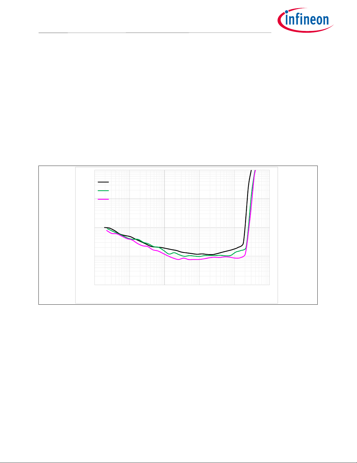
4.7.3 Frequency response
Test conditions:
Output power = 1 W, LPF = 22uH+0.47uF
4
2ohm
2
0
-2
dBr A
-4
3ohm
4ohm
6ohm
Frequency(Hz)
Figure 4 Frequency response
Datasheet 16 of 59 V 2.0
9/24/2021
-6
-8
-10
20 200 2000 20000 200000
Frequency(Hz)

MA
5332MS
Table of contents
Integrated Class D Amplifier
4.7.4 Noise floor
10
-10
-30
-50
dBV
-70
-90
-110
-130
-150
10 100 1000 10000
Figure 5 Noise floor
4.7.5 Efficiency
2ohm
3ohm
4ohm
6ohm
Frequency(Hz)
100.0%
90.0%
80.0%
70.0%
60.0%
50.0%
40.0%
Efficiency
30.0%
20.0%
10.0%
0.0%
0.00 50.00 100.00 150.00 200.00 250.00
Figure 6 Efficiency 4 Ω load
MA5332 4ohm load
MA5332 4ohm load
Power (W)
Datasheet 17 of 59 V 2.0
9/24/2021
MA
5332MS
Table of contents
10
Integrated Class D Amplifier
4.8 Typical Audio characteristics (BTL)
Test conditions:
All Measurements taken at Sine wave frequency= 1 kHz, AES17+ AUX-0025 measurement filters.
V
= ± 40 V, Load impedance = 8 Ω, F
bus
V
= ± 31.5 V, Load impedance = 6 Ω, F
bus
V
= ± 23 V, Load impedance = 4 Ω, F
bus
= 400 kHz
PWM
= 400 kHz
PWM
= 400 kHz
PWM
4.8.1 Power vs. THD+N
4ohm
6ohm
1
0.1
THD+N(%)
0.01
0.001
0.01 0.1 1 10 100 1000
8ohm
Figure 7 Power vs. THD+N
Outpower(W)
Datasheet 18 of 59 V 2.0
9/24/2021
 Loading...