ITS 4140N
Smart High-Side Power Switch
for Industrial Applications
One channel: 1 x 1 Ω
Features
• Current controlled input
• Short circuit protection
Product Summary
Overvoltage protection V
Operating voltage V
On-state resistance RON 1
• Current limitation
Operating Temperature T
• Overload protection
• Overvoltage protection (including load dump)
• Switching inductive loads
• Clamp of negative voltage at output with inductive loads
• Thermal shutdown with restart
• ESD – Protection
• Loss of GND and loss of Vbb protection
• Very low standby current
• Reverse battery protection
• Improved electromagnetic compatibility (EMC)
62 V
bbin(AZ)
4,9...60 V
bb(on)
a
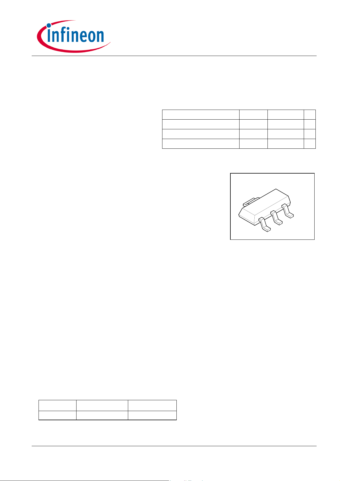
PG-SOT223
4
Ω
-30 … +85 °C
3
2
1
Application
• All types of resistive, inductive and capacitive loads in industrial applications
• Current controlled power switch for 12V, 24V and 42V DC industrial applications
• Driver for electromagnetic relays
• Signal amplifier
General Description
• N channel vertical power MOSFET with charge pump and current controlled input,
monolithically integrated in Smart SIPMOS® technology.
• Providing embedded protection functions.
Type
ITS 4140N SP000240073
Ordering code Package
PG-SOT223
Datasheet Page 1 Rev. 2.1, 2006-07-24
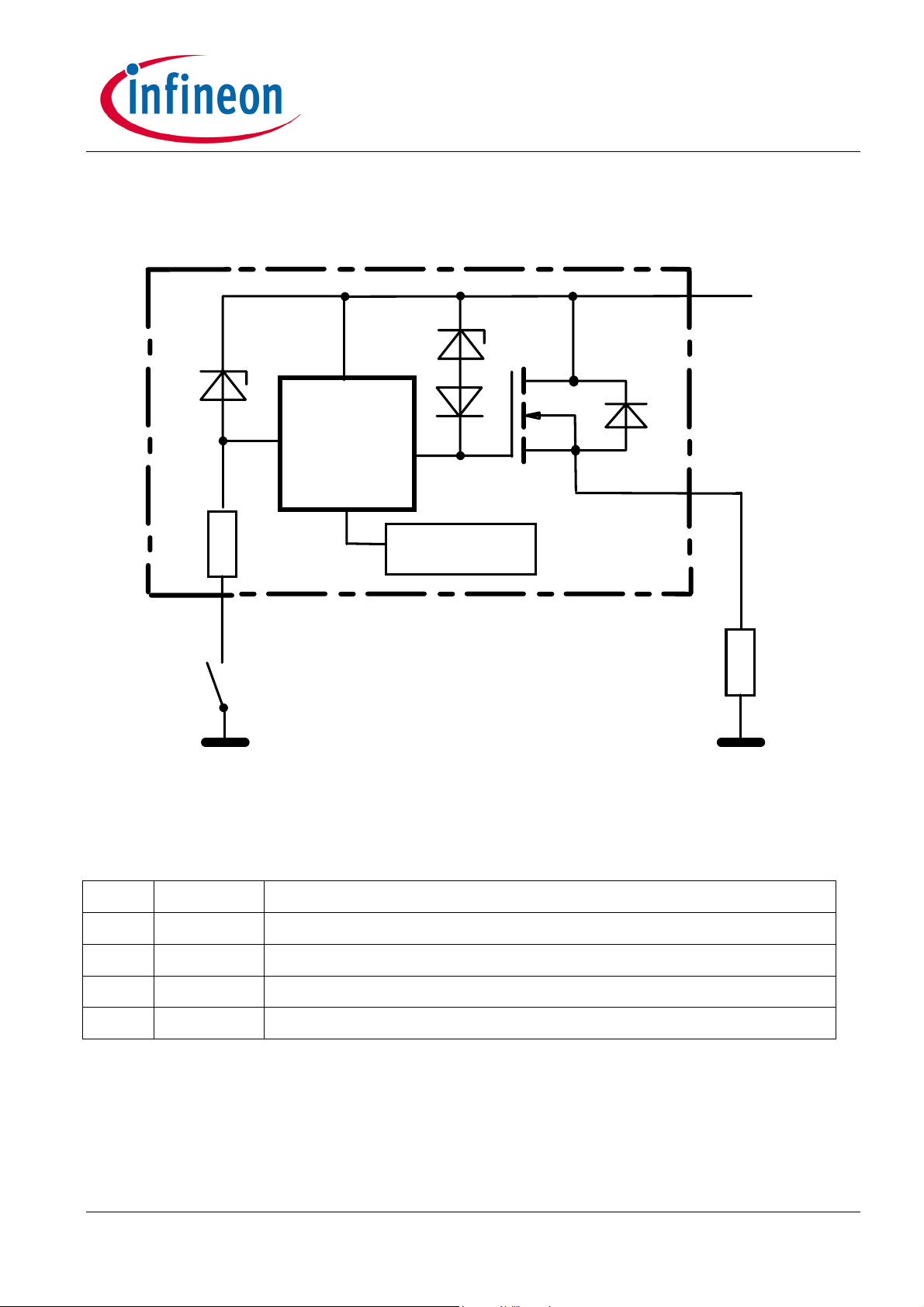
Block Diagram
ITS 4140N
+ V
bb
2/4
Control
Circuit
Temperature
Sensor
IN
R
IN
1
GND
Pin Symbol Function
OUT
3
R
L
1 IN Input, activates the power switch in case of connection to GND
2 Vbb Positive power supply voltage
3 OUT Output to the load
4 Vbb Positive power supply voltage
Datasheet Page 2 Rev. 2.1, 2006-07-24

Maximum Ratings
ITS 4140N
Parameter
Symbol Values Unit
at Tj = 25°C unless otherwise specified
Supply voltage Vbb 60 V
Load current (Short – circuit current, see page 5) IL self limited A
Maximum current through the input pin (DC) IIN ±15 mA
Junction temperature
Operating temperature range
Storage temperature range
Power dissipation1)
Tj
T
a
T
stg
P
1.7 W
tot
+150
-30 … +85
-40 ...+105
°C
Ta = 25 °C
Inductive load switch-off energy dissipation2)
Single pulse
E
AS
1 J
Tj = 150°C, IL = 0.15A
Load dump protection3) V
LoadDump
RL=2Ω, td = 400ms, VIN = low or high
IL = 150mA, Vbb = 13.5V
Vbb = 27V
4)
= VA + VS
V
LoadDump
93.5
127
V
Electrostatic discharge voltage (Human Body Model)
According to ANSI EOS/ESD – S5.1 – 1993
ESD STM5.1 – 1998
Input pin
all other pins
V
ESD
±1
±5
1
Device on 50mm*50mm*1.5mm epoxy PCB FR4 with 6 cm2 (one layer, 70µm thick) copper area for V
connection. PCB is vertical without blown air.
2
Not subject to production test, specified by design
3
More details see EMC-Characteristics on page 7
4
V
LoadDump
is setup without the DUT connected to the generator per ISO 7637-1 and DIN 40839.
kV
bb
Datasheet Page 3 Rev. 2.1, 2006-07-24
ITS 4140N
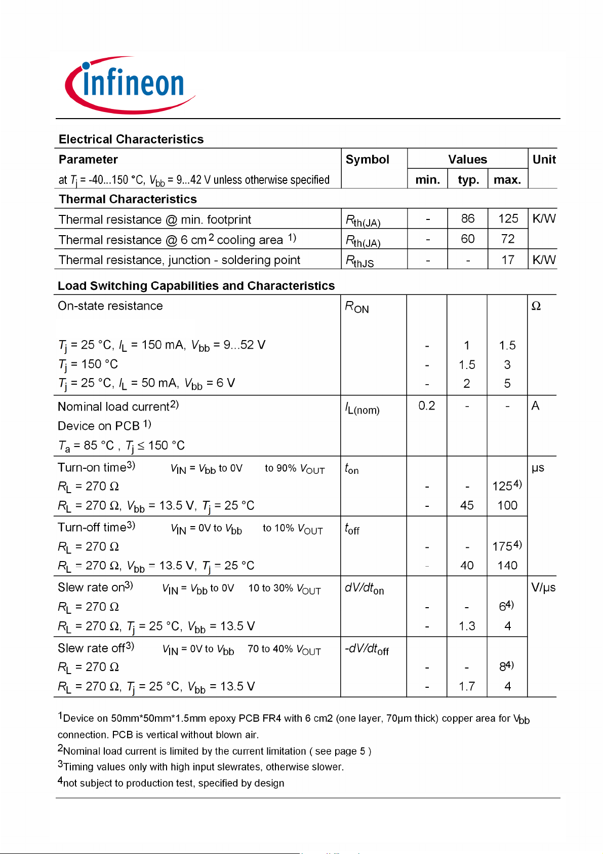
Pin1 connected to GND
Datasheet Page 4 Rev. 2.1, 2006-07-24
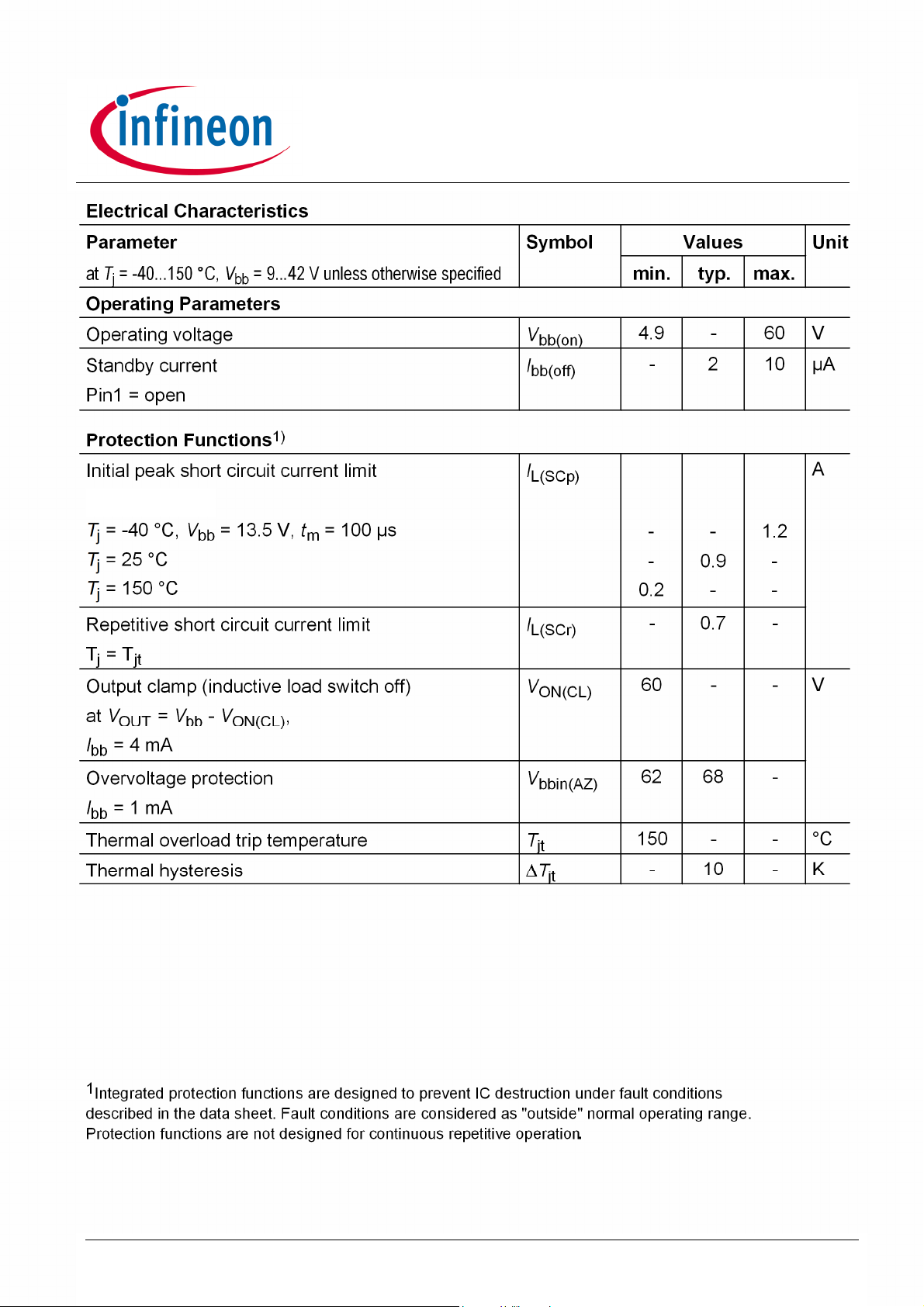
(see page 14)
ITS 4140N
Datasheet Page 5 Rev. 2.1, 2006-07-24
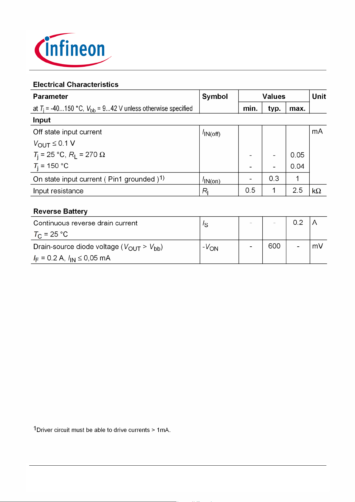
ITS 4140N
Datasheet Page 6 Rev. 2.1, 2006-07-24
 Loading...