


/
IRLHS6276PbF
HEXFET® Power MOSFET
V
DS
V
GS
R
DS(on) max
(@VGS = 4.5V)
R
DS(on) max
(@VGS = 2.5V)
I
D
(@T
c(Bottom)
= 25°C)
20 V
12 V
±
45
62 m
3.4
d
m
7239,(
:
Ω
Ω
A
6
*
'
)(7
)(7
'
'
*
'
6
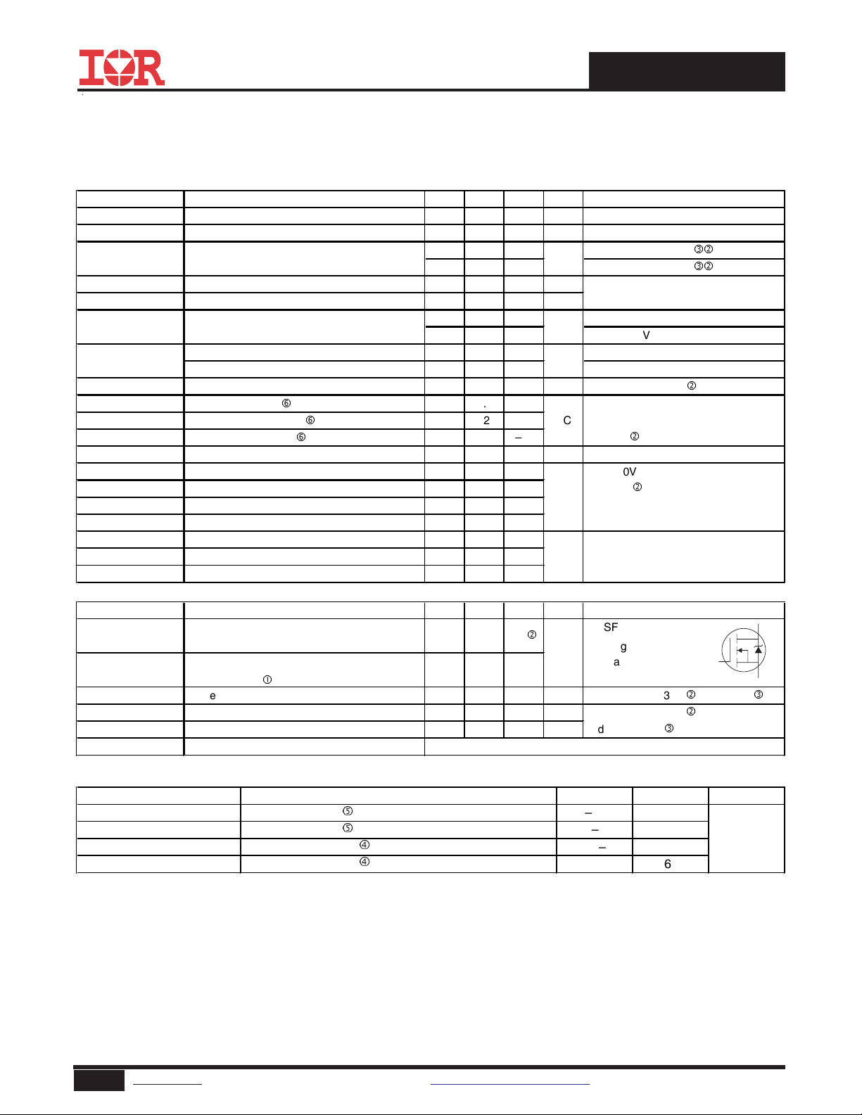
2mm x 2mm Dual PQFN
G2
S2
Applications
• Charge and discharge switch for battery application
• Load/System Switch
Features and Benefits
Features Resulting Benefits
Low R
Low Thermal Resistance to PCB (≤ 19°C
Low Profile (≤ 1.0mm) results in Increased Power Density
Industry-Standard Pinout
Compatible with Existing Surface Mount Techniques Easier Manufacturing
RoHS Compliant Containing no Lead, no Bromide and no Halogen Environmentally Friendlier
(≤ 45mΩ) Lower Conduction Losses
DSon
W) Enable better thermal dissipation
⇒
Multi-Vendor Compatibility
D1
D1
D2
S1
G1
D2
Orderable part number Package Type Standard Pack
Form Quantity
IRLHS6276TRPBF PQFN Dual 2mm x 2mm Tape and Reel 4000
IRLHS6276TR2PBF
PQFN Dual 2mm x 2mm Tape and Reel 400 EOL notice #259
Absolute Maximum Ratings
Parameter Units
V
DS
V
GS
@ TA = 25°C
I
D
I
@ TA = 70°C
D
I
@ T
D
I
@ T
D
I
@ T
D
I
DM
PD @TA = 25°C
PD @T
T
J
T
STG
C(Bottom)
C(Bottom)
C(Bottom)
C(Bottom)
= 25°C
= 100°C
= 25°C
= 25°C
Notes through are on page 2
Drain-to-S ource Voltage
Gate-to-Source Voltage
Continuous Drain Current, V
Continuous Drain Current, V
Continuous Drain Current, V
Continuous Drain Current, V
Continuous Drain Current, V
Pulsed Drain Current
Power Dissipation
Power Dissipation
Linear Derating Factor
Operating Junction and
Storage Temperature Range
c
f
f
f
@ 4.5V
GS
@ 4.5V
GS
@ 4.5V
GS
@ 4.5V
GS
@ 4.5V (Package Limited)
GS
Max.
20
±12
d
4.5
d
3.6
d
9.6
d
6.1
d
3.4
40
1.5
6.6
0.012
-55 to + 150
Note
V
A
W
W/°C
°C
1 www.irf.com © 2014 International Rectifier Submit Datasheet Feedback January 13, 2014
Th
l Resist
Static @ TJ = 25°C (unless otherwise specified)
–
(
)
Parameter Min. Typ. Max. Units
BV
DSS
/∆T
∆ΒV
DSS
J
R
DS(on)
V
GS(th)
∆V
GS(th)
I
DSS
I
GSS
gfs Forward Transconductance 8.8 ––– ––– S
Q
g
Q
gs
Q
gd
R
G
t
d(on)
t
r
t
d(off)
t
f
C
iss
C
oss
C
rss
Drain-to-Source Breakdown Voltage 20 ––– ––– V
Breakdown Voltage Temp. Coefficient ––– 9.3 ––– mV/°C
Static Drain-to-Source On-Resistance ––– 33 45
––– 46 62
mΩ
Gate Threshold Voltage 0.5 0.8 1.1 V
Gate Threshold Voltage Coefficient ––– -3.8 ––– mV/°C
Drain-to-Source Leakage Current ––– ––– 1.0
––– ––– 150
Gate-to-Source Forward Leakage ––– ––– 100
Gate-to-Source Reverse Leakage ––– ––– -100
Total Gate Charge
Gate-to-Source Charge
Gate-to-Drain Charge
h
h
h
Gate Resistance ––– 4.0
––– 3.1 –––
–––0.22–––
––– 1.3 –––
––
Turn-On Delay Time ––– 4.4 –––
Rise Time ––– 9.3 –––
Turn-Off Delay Time ––– 10 –––
Fall Time ––– 4.9 –––
Input Capacitance ––– 310 –––
Output Capacitance ––– 79 –––
Reverse Transfer Capacitance ––– 49 –––
Diode Characteristics
Parameter Min. Typ. Max. Units
I
S
I
SM
V
SD
t
rr
Q
rr
t
on
Continuous Source Current
(Body Diode)
Pulsed Source Current
Body Diode
c
––– ––– 9.6
––– ––– 40
d
Diode Forward Voltage ––– ––– 1.2 V
Reverse Recovery Time ––– 5.2 7.8 ns
Reverse Recovery Charge ––– 5.0 7.5 nC
Forward Turn-On Time Time is dominated by parasitic Inductance
IRLHS6276PbF
Conditions
VGS = 0V, ID = 250µA
Reference to 25°C, I
= 4.5V, ID = 3.4A
V
GS
= 2.5V, ID = 3.4A
V
GS
= VGS, ID = 10µA
V
DS
= 16V, VGS = 0V
V
DS
µA
VDS = 16V, VGS = 0V, TJ = 125°C
= 12V
V
GS
nA
nC
Ω
ns
pF
A
= -12V
V
GS
= 10V, ID = 3.4A
V
DS
V
= 10V
DS
= 4.5V
V
GS
= 3.4Ad (See Fig.17 & 18)
I
D
V
= 10V, VGS = 4.5V
DD
G
=1.8
d
Ω
ID = 3.4A
R
See Fig.15
VGS = 0V
= 10V
V
DS
ƒ = 1.0MHz
Conditions
MOSFET symbol
showing the
integral reverse
p-n junction diode.
TJ = 25°C, IS = 3.4Ad, VGS = 0V
T
= 25°C, IF = 3.4Ad, VDD = 10V
J
di/dt = 126A/µs
e
= 1mA
D
ed
ed
d
D
G
S
e
erma
ance
Parameter Typ. Max. Units
R
JC
θ
R
θJC
R
JA
θ
R
θJA
Notes:
(Bottom)
(Top)
(<10s)
Junction-to-Case
Junction-to-Case
Junction-to-Ambient
Junction-to-Ambient
g
g
f
f
––– 19
––– 175
––– 86
––– 69
°C/W
Repetitive rating; pulse width limited by max. junction temperature.
Current limited by package.
Pulse width ≤ 400µs; duty cycle ≤ 2%.
When mounted on 1 inch square copper board.
R
is measured at T
θ
of approximately 90°C.
J
For DESIGN AID ONLY, not subject to production testing.
2 www.irf.com © 2014 International Rectifier Submit Datasheet Feedback January 13, 2014
IRLHS6276PbF
100
TOP 10V
)
A
(
10
t
n
e
r
r
u
C
e
c
r
1
u
o
S
o
t
n
i
a
r
0.1
D
,
D
I
1.4V
≤
BOTTOM 1.4V
60µs PULSE WIDTH
Tj = 25°C
0.01
0.1 1 10 100
VDS, Drain-to-Source Voltage (V)
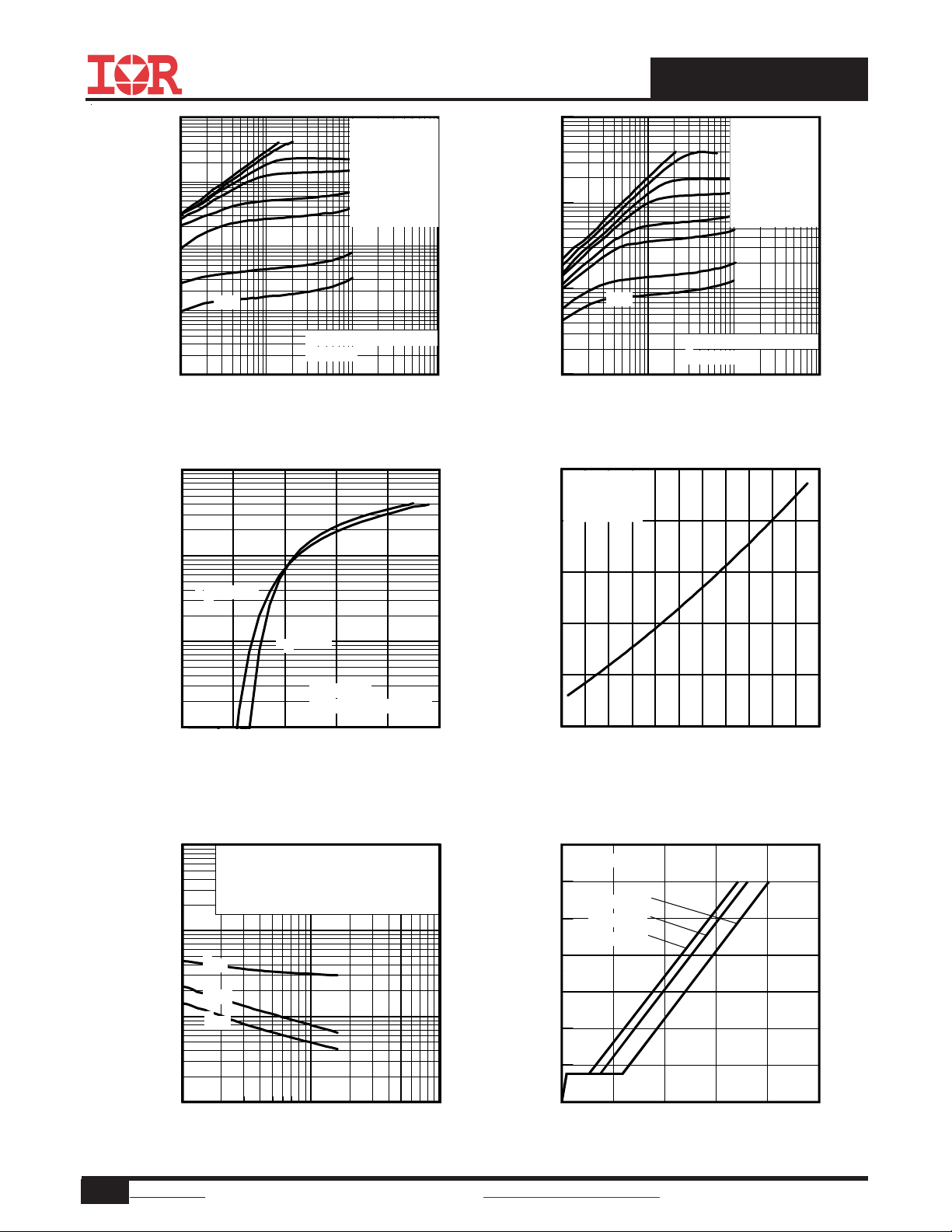
Fig 1. Typical Output Characteristics
100
)
A
(
t
n
e
r
10
r
u
C
e
c
r
u
o
S
o
t
n
i
a
r
D
,
D
I
TJ = 150°C
1
TJ = 25°C
V
DS
≤
60µs PULSE WIDTH
= 10V
0.1
0.0 1.0 2.0 3.0 4.0 5.0
VGS, Gate-to-Source Voltage (V)
VGS
4.5V
3.0V
2.5V
2.0V
1.8V
1.5V
100
)
A
(
t
n
e
r
10
r
u
C
e
c
r
u
o
S
o
t
-
1
n
i
a
r
D
,
D
I
1.4V
60µs PULSE WIDTH
≤
Tj = 150°C
0.1
0.1 1 10 100
VDS, Drain-to-Source Voltage (V)
Fig 2. Typical Output Characteristics
1.6
e
c
n
a
t
s
i
s
e
R
n
O
e
c
r
u
o
S
o
t
n
i
a
r
D
,
)
n
o
(
S
D
R
ID = 3.4A
V
= 4.5V
GS
1.4
)
1.2
d
e
z
i
l
a
m
r
1.0
o
N
(
0.8
0.6
-60 -40 -20 0 20 40 60 80 100 120140 160
TJ , Junction Temperature (°C)
TOP 10V
BOTTOM 1.4V
VGS
4.5V
3.0V
2.5V
2.0V
1.8V
1.5V
Fig 3. Typical Transfer Characteristics
10000
)
F
p
(
e
c
n
a
t
i
c
a
p
a
C
,
C
1000
100
10
V
= 0V, f = 1 MHZ
GS
C
= C
= C
= C
+ Cgd, C
gs
gd
+ C
ds
iss
C
rss
C
oss
C
iss
C
oss
C
rss
SHORTED
ds
gd
1 10 100
VDS, Drain-to-Source Voltage (V)
Fig 4. Normalized On-Resistance vs. Temperature
14.0
ID= 3.4A
12.0
)
V
(
e
g
10.0
a
t
l
o
V
e
8.0
c
r
u
o
S
-
6.0
o
t
e
t
a
4.0
G
,
S
G
V
2.0
0.0
VDS= 16V
VDS= 10V
VDS= 4.0V
0246810
QG, Total Gate Charge (nC)
Fig 6. Typical Gate Charge vs.Gate-to-Source VoltageFig 5. Typical Capacitance vs.Drain-to-Source Voltage
3 www.irf.com © 2014 International Rectifier Submit Datasheet Feedback January 13, 2014
 Loading...