


INFINEON IRLHS6242PBF Datasheet
Absolute Maximum Ratings
GS
D
D
D
Continuous Drain Current, VGS @ 4.5V
i
DM
Pulsed Drain Current
c
Power Dissipation
g
Power Dissipation
g
Linear Derating Factor
W/°C
J
STG
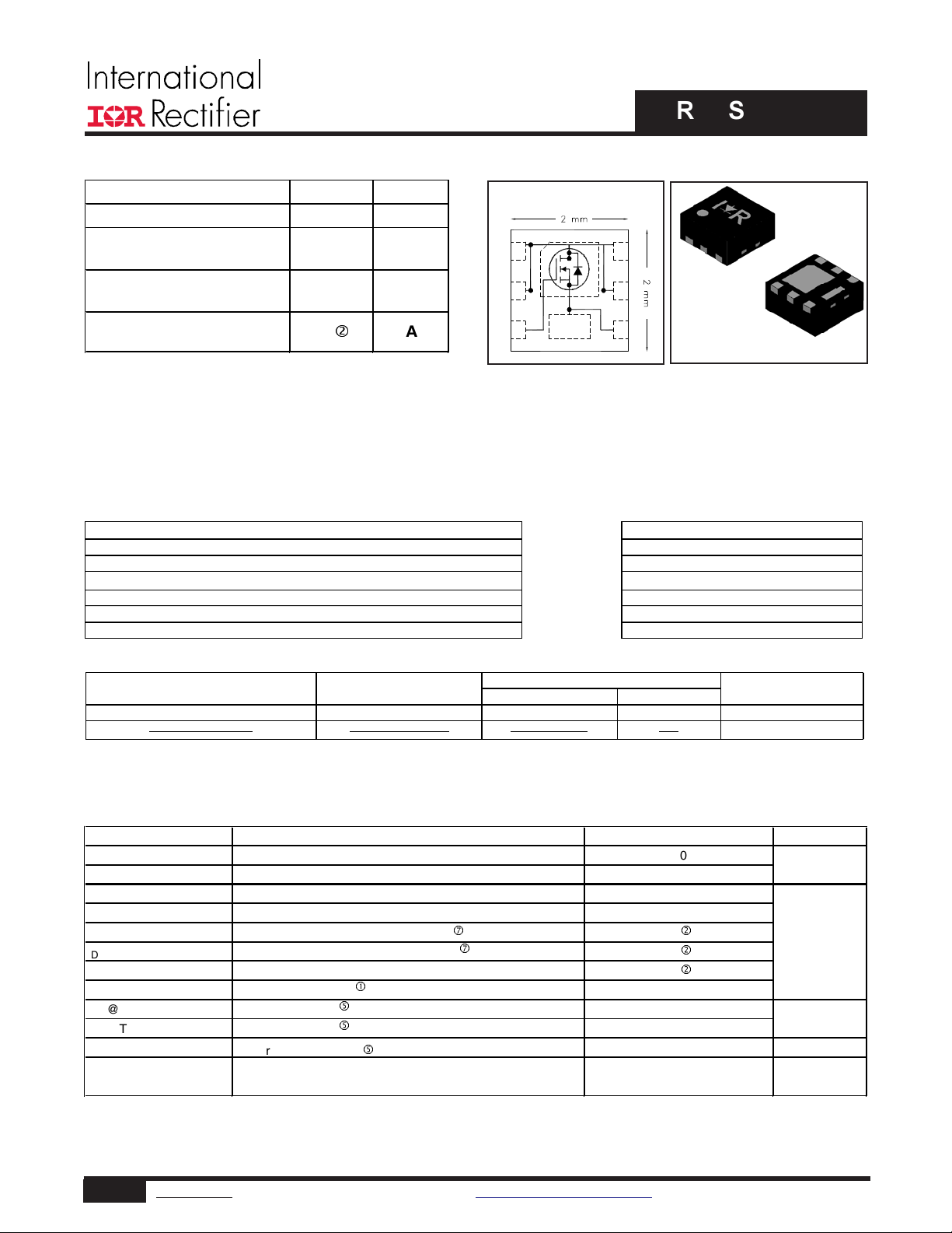
IRLHS6242PbF
IRLHS6242TRPbF
PQFN 2mm x 2mm
Tape and Reel
4000
Standard Pack
DSon
Ω)
≤
≤
HEXFET® Power MOSFET
V
DS
V
GS
R
DS(on) max
(@VGS = 4.5V)
R
DS(on) max
(@VGS = 2.5V)
I
D
(@T
C (Bottom)
= 25°C)
20 V
12 V
±
11.7 m
15.5
12
d
mΩ
TOP VIEW
Ω
A
D1
D2
G 3
S
6D
5D
D
4S
2mm x 2mm PQFN
Applications
• Charge and discharge switch for battery application
• System/Load Switch
Features and Benefits
Features Resulting Benefits
Low R
Low Thermal Resistance to PCB (
Low Profile (
Industry-Standard Pinout
Compati ble with Existing Surf ac e Mount Techniques
RoHS Compliant Containing no Lead, no Bromide and no Halogen
MSL1, Industrial Qualification Increased Reliability
(≤ 11.7m
13°C/W) Enable better thermal dissipation
1.0mm) results in Increased Power Density
⇒
Lower Conduction Losses
Multi-Vendor Compatibility
Easier Manufacturing
Environmentally Friendlier
D
D
D
D
D
S
G
S
Orderable part number Package Type
IRLHS6242TR2PbF PQFN 2mm x 2mm Tape and Reel 400
V
DS
V
I
@ TA = 25°C
@ TA = 70°C
I
@ T
I
C(Bottom)
ID @ T
C(Bottom)
ID @ T
C(Bottom)
I
PD @TA = 25°C
PD @T
C(Bottom)
T
T
= 25°C
= 70°C
= 25°C
= 25°C
Parameter Units
Drain-to-Source Voltage
Gate-to-Source Voltage
Continuous Drain Current, V
Continuous Drain Current, V
Continuous Drain Current, V
Continuous Drain Current, V
g
Operating Junction and
Storage Temperature Range
@ 4.5V
GS
@ 4.5V
GS
@ 4.5V
GS
@ 4.5V (Package Limited)
GS
i
Form Quantity
Max.
20
±12
10
8.3
22
18
12
88
1.98
9.6
0.016
-55 to + 150
Note
EOL notice # 259
V
d
d
d
A
W
°C
Notes through are on page 2
1 www.irf.com © 2013 International Rectifier Submit Datasheet Feedback December 17, 2013
Static @ TJ = 25°C (unless otherwise specified)
ΔΒ
Δ
–––
Diode Characteristics
(Body Diode)
Thermal Resistance
R
θ
JC
(Bottom)
Junction-to-Case
g
–––
13
θ
JC
Junction-to-Case
g
θ
JA
Junction-to-Ambient
f
R
θ
JA
(<10s)
Junction-to-Ambient
f
–––
46
Parameter Min. Typ. Max. Units
BV
DSS
V
/ΔT
DSS
J
R
DS(on)
V
GS(th)
V
GS(th)
I
DSS
I
GSS
gfs Forward Transconductance 36 ––– ––– S
Q
g
Q
gs
Q
gd
R
G
t
d(on)
t
r
t
d(off)
t
f
C
iss
C
oss
C
rss
Drain-to-Source Breakdown Voltage 20 ––– ––– V
Breakdown Voltage Temp. Coefficient ––– 6.8 ––– mV/°C
Static Drain-to-Source On-Resistance ––– 9.4 11.7
––– 12.4 15.5
mΩ
Gate Threshold Voltage 0.5 0.8 1.1 V
Gate Threshold Voltage Coefficient ––– -4.2 ––– mV/°C
Drain-to-Source Leakage Current ––– ––– 1.0
––– ––– 150
Gate-to-Source Forward Leakage ––– ––– 100
Gate-to-Source Reverse Leakage ––– ––– -100
Total Gate Charge
h
Gate-to-Source Charge
Gate-to-Drain Charge
h
h
––– 14 –––
––– 1.5 –––
––– 6.3 –––
Gate Resistance ––– 2.1
Turn-On Delay Time ––– 5.8 –––
Rise Time ––– 15 –––
Turn-Off Delay Time ––– 19 –––
Fall Time ––– 13 –––
Input Capacitance ––– 1110 –––
Output Capacitance ––– 260 –––
Reverse Transfer Capacitance ––– 180 –––
IRLHS6242PbF
Conditions
VGS = 0V, ID = 250μA
Reference to 25°C, I
= 4.5V, ID = 8.5A
V
GS
= 2.5V, ID = 8.5A
V
GS
V
= VGS, ID = 10μA
DS
= 16V, VGS = 0V
V
DS
μA
VDS = 16V, VGS = 0V, TJ = 125°C
= 12V
V
GS
nA
nC
Ω
ns
pF
= -12V
V
GS
= 10V, ID = 8.5A
V
DS
V
= 10V
DS
= 4.5V
V
GS
I
= 8.5Ad (See Fig.17 & 18)
D
V
= 10V, VGS = 4.5V
DD
G
=1.8
d
Ω
ID = 8.5A
R
See Fig.15
VGS = 0V
= 10V
V
DS
ƒ = 1.0MHz
= 1mA
D
ed
ed
d
e
Parameter Min. Typ. Max. Units
I
S
I
SM
V
SD
t
rr
Q
rr
t
on
Continuous Source Current
(Body Diode)
Pulsed Source Current
c
––– ––– 22
––– ––– 88
Diode Forward Voltage ––– ––– 1.2 V
Reverse Recovery Time ––– 15 23 ns
Reverse Recovery Charge ––– 12 18 nC
Forward Turn-On Time Time is dominated by parasitic Inductance
Parameter Typ. Max. Units
R
(Top)
R
Notes:
Repetitive rating; pulse width limited by max. junction temperature.
Package is limited to 12A by die-source to lead-frame bonding technology.
Pulse width ≤ 400μs; duty cycle ≤ 2%.
When mounted on 1 ich square copper board.
R
is measured at T
θ
of approximately 90°C.
J
For DESIGN AID ONLY, not subject to production testing.
Calculated continuous current based on maximum allowable junction temperature.
Conditions
MOSFET symbol
showing the
A
integral reverse
p-n junction diode.
TJ = 25°C, IS = 8.5Ad, VGS = 0V
T
= 25°C, IF = 8.5Ad, VDD = 10V
J
di/dt = 210A/μs
e
––– 94
––– 63
D
G
S
e
°C/W
2 www.irf.com © 2013 International Rectifier Submit Datasheet Feedback December 17, 2013
IRLHS6242PbF
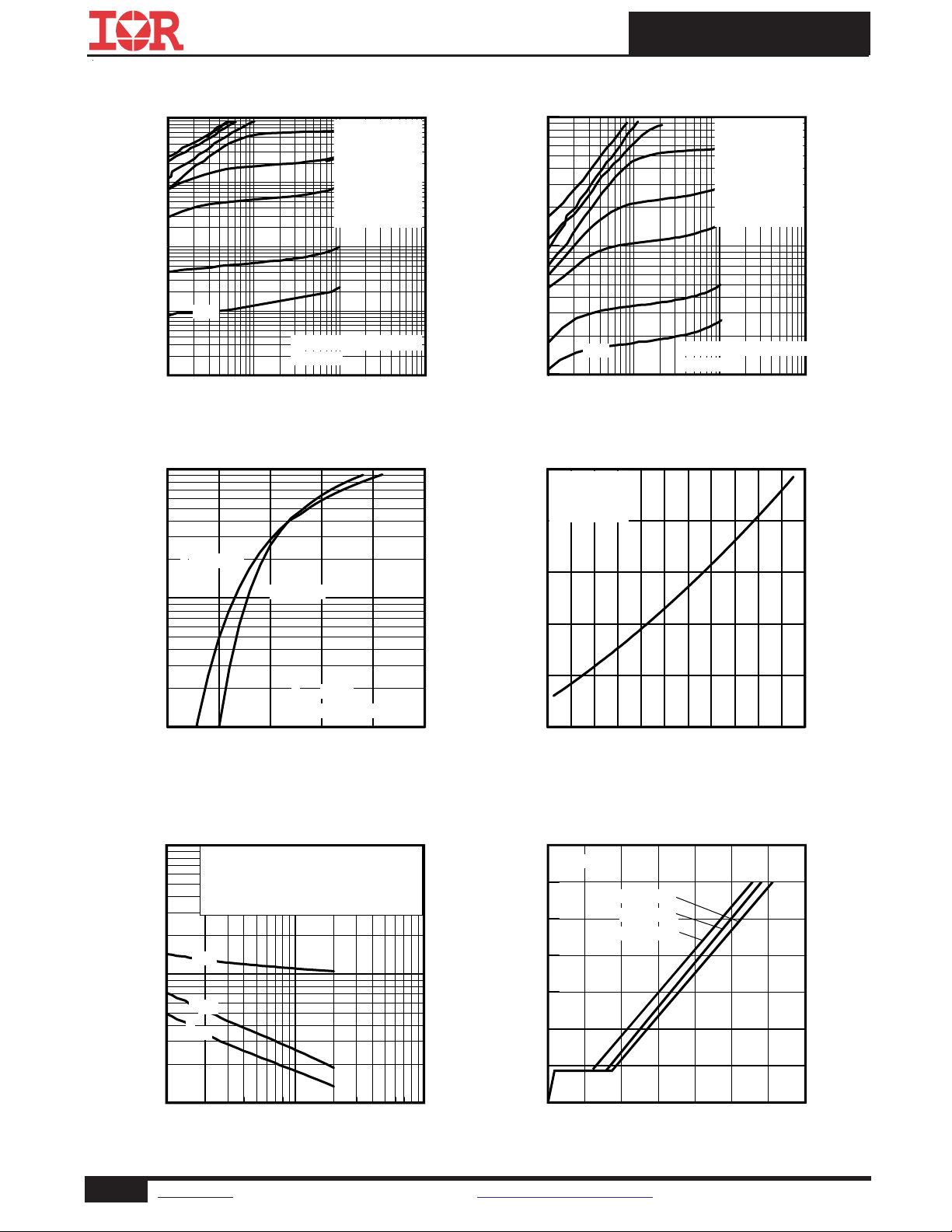
100
TOP 10V
)
A
(
10
t
n
e
r
r
u
C
e
c
r
1
u
o
S
o
t
n
i
a
r
0.1
D
,
D
I
1.4V
≤
BOTTOM 1.4V
60μs PULSE WIDTH
Tj = 25°C
0.01
0.1 1 10 100
VDS, Drain-to-Source Voltage (V)
Fig 1. Typical Output Characteristics
100
)
A
(
t
n
e
r
r
u
C
e
c
r
u
o
S
o
t
n
i
a
r
D
,
D
I
TJ = 150°C
10
TJ = 25°C
V
= 10V
DS
≤
60μs PULSE WIDTH
1.0
1.0 1.5 2.0 2.5 3.0 3.5
VGS, Gate-to-Source Voltage (V)
VGS
4.5V
3.0V
2.5V
2.0V
1.8V
1.5V
100
)
A
(
t
n
e
r
r
u
C
e
c
r
10
u
o
S
o
t
n
i
a
r
D
,
D
I
60μs PULSE WIDTH
1.4V
1
≤
Tj = 150°C
0.1 1 10 100
VDS, Drain-to-Source Voltage (V)
Fig 2. Typical Output Characteristics
1.6
e
c
n
a
t
s
i
s
e
R
n
O
e
c
r
u
o
S
o
t
n
i
a
r
D
,
)
n
o
(
S
D
R
ID = 8.5A
V
= 4.5V
GS
1.4
)
1.2
d
e
z
i
l
a
m
r
1.0
o
N
(
0.8
0.6
-60 -40 -20 0 20 40 60 80 100 120 140160
TJ , Junction Temperature (°C)
TOP 10V
BOTTOM 1.4V
VGS
4.5V
3.0V
2.5V
2.0V
1.8V
1.5V
Fig 3. Typical Transfer Characteristics
10000
)
F
p
(
e
c
n
a
t
i
c
a
p
a
C
,
C
1000
100
V
= 0V, f = 1 MHZ
GS
C
= C
= C
= C
+ Cgd, C
gs
gd
+ C
ds
iss
C
rss
C
oss
C
iss
C
oss
C
rss
SHORTED
ds
gd
1 10 100
VDS, Drain-to-Source Voltage (V)
Fig 5. Typical Capacitance vs.Drain-to-Source Voltage
Fig 4. Normalized On-Resistance vs. Temperature
14.0
ID= 8.5A
12.0
)
V
(
e
g
10.0
a
t
l
o
V
e
8.0
c
r
u
o
S
-
6.0
o
t
e
t
a
4.0
G
,
S
G
V
2.0
VDS= 16V
VDS= 10V
VDS= 4.0V
0.0
0 5 10 15 20 25 30 35
QG, Total Gate Charge (nC)
Fig 6. Typical Gate Charge vs.Gate-to-Source Voltage
3 www.irf.com © 2013 International Rectifier Submit Datasheet Feedback December 17, 2013